
Abstract
This work proposes a simple simulation method for the optimization of n-i-p perovskite solar cell (PSCs) via SCAPS-1D and aims to achieve high-performance devices. Nowadays, the carrier recombination induced by heavy defects in bulk and interfaces is one of the main obstacles which restricts PSC efficiency and is also harmful to device stability. Here we modify the MAPbI3 device through a series of structural and basic optimizations, including the thickness of each layer, carrier diffusion length, interface recombination, doping concentration and overall series resistance. Through the modified simulation, a high-performance MAPbI3 device with suppressed recombination and optimized structure is realized, resulting in an encouraging power conversion efficiency of 20.09%, an enhanced Voc of 1.087 V, Jsc of 22.56 mA cm−2 and an FF of 78.5%. These findings unveil the critical effect of defect suppression on PSCs and offer a simple method to achieve high-performance devices.
Export citation and abstract BibTeX RIS
1. Introduction
As a renewable and eco-friendly energy, solar energy is a prospective substitution for traditional energy in the future. Therefore, 3rd generation solar cells, especially perovskite solar cells (PSCs) have become a prevalent trend for worldwide researchers in recent years owing to their superior opto-electronic properties, including high absorption coefficient, tunable band gap and high charge carrier mobility, etc. 1,2) In 2012, Park et al. introduced an all-solid-state structure PSC with an encouragingly improved stability, which utilized mesoporous TiO2 as the electron transport layer (ETL) and Spiro-OMeTAD as the hole transport layer (HTL), to substitute the electrolyte in the dye-sensitized cell. 3) The new mesoporous heterojunction structure achieved long-term stability over 500 h without encapsulation. Simultaneously, the solution-processable PSCs with an excellent mesoporous Al2O3 scaffold beneficial for perovskite growth resulted in a power conversion efficiency (PCE) of over 10%, which emerged rapidly and afterward grew very fast in the photovoltaic field within a decade. 4)
As the most typical organic-inorganic hybrid perovskite material, MAPbI3 performs a desirable energy bandgap and exhibits great potential in obtaining high-performance devices. To date, the commonly used one-step solution method achieved a record PCE of over 18% for pure MAPbI3 PSCs. 5) Up to now, plenty of approaches have been developed for device modification, including additive engineering, interface passivation such as various Lewis bases, for example, IDIC, PVP and PCDTBT, energy level engineering and fabrication methodology. 6–8) For example, Zhang and his co-workers reported an effective additive engineering strategy by doping formamidinium iodide in MAPbI3 film to regulate the crystallization and suppress the defect density of perovskite film. 9) In 2020, Li et al. introduced a facile method to modify the PEDOT:PSS layer with sodium benzenesulfonate (C6H5SO3Na) as a well-matched energy level alignment structure in commonly inverted PSCs. 10) Recently, a tetragonal (200) oriented MAPbI3 film has been obtained by the screening hot-casting technique, which achieved less trap density and accelerated charge transfer in the absorber layer. 11) In summary, the MAPbI3-based PSCs have been successfully developed in PCE due to the efforts by masses of researchers and promote the future commercialization for PSCs.
Despite the most rapid developments for PSCs in the photovoltaic community, there is a certain discrepancy between the experimental and theoretical PCE which is ∼30.5% in prediction according to Shockley–Queisser Limit. 12) The heavy defect density in the configuration of PSCs is one of the main reasons to undermine their performance, finally leading to the huge efficiency discrepancy. 13) In this work, we analyze the J–V characteristics of the MAPbI3 device via the Solar Cell Capacitance Simulator (SCAPS) simulation and come up with a simple optimization strategy using an interface engineering method to improve device performance. 14) The SCAPS is a one-dimensional solar cell simulator developed with LabWindows/CVI from the University of Gent and utilized in different organic and inorganic thin film devices, such as silicon, CIGS, CdTe and PSCs. 15) Herein, the investigation is focused on the analysis of planar n-i-p structure PSCs by changing the configuration parameters of the simulation, including thicknesses of each layer, defect density, interface recombination, doping concentration, and the series and shunt resistances. Moreover, two interface defect layers (IDLs) of 10 nm are inserted between ETL/perovskite and perovskite/HTL to compute the interface recombination.
2. Experimental methods
2.1. Material preparation
All the reagents were used as received without further purification. Methylamine iodide (MAI, > 99.99%), lead iodide (PbI2, > 99.99%), 2,2',7,7'-tetrakis (N, N-di-p-methoxyphenylamine)-9,9'-spirobifluorene (Spiro-OMeTAD, >99.5%), tris (2-(1H-pyrazol-1-yl)-4-tert-butylpyridine)-cobalt (Ⅲ) tris (bis-(trifluoromethylsulphonyl) imide) (FK209, > 99%), bis(trifluoromethance) sulfonimide lithium salt (LiTFSI, > 99%) and 4-tert-butylpyridine (4-TBP, > 96%) were purchased from Tokyo Chemical Industry Co., Japan. The SnO2 colloid solution (tin (Ⅳ) oxide) was obtained from Alfa Aesar. Other chemicals were provided by Wako Co., Japan.
2.2. Preparation of SnO2 ETL on FTO Substrate
Fluorine-doped tin oxide (FTO) conducting glass substrates (sheet resistance of 10 Ω sq−1) were sequentially washed by ultrasonication in detergent solution, deionized water, ethyl alcohol, acetone and isopropanol for 20 min, respectively. The SnO2 colloid solution (15%) was diluted with deionized water to the concentration of 5 wt%. Before ETLs deposition, the cleaned FTO substrates were dried with nitrogen and treated by UV-ozone for 30 min. The colloid precursor of SnO2 was spin-coated onto FTO substrate at 3000 rpm for 20 s. The substrate was then annealed at 150 °C for 30 min to obtain the SnO2 film.
2.3. Solar cell fabrication and characterization
After the preparation for ETLs, the substrates were moved into a glove box filled with N2 for perovskite, HTL deposition and electrode evaporation. The MAPbI3 perovskite layers were fabricated by a one-step method as reported. 553 mg PbI2 and 190 mg MAI were dissolved in 1 ml mixed DMF/DMSO (4:1) solvent and stirred for one night at 50 °C. After that, 100 μl of the precursor was spin-coated onto the FTO/SnO2 substrate at 1000 rpm for 12 s and 5000 rpm for 30 s, respectively. During the high-speed spin-coating process, 200 μl antisolvent was dripped on the perovskite film after 7 s to promote the perovskite crystallization. Subsequently, the substrates were annealed at 100 °C for 10 min to form uniform and compact films. For HTL, the mixture of 72 mg Spiro-OMeTAD, 14 μl FK209 (376 mg ml−1 in acetonitrile), 17 μl Li-TFSI (520 mg ml−1 in acetonitrile) and 29 μl 4-TBP dissolved in 1 ml CB was spin-coated onto perovskite film at 4000 rpm for 20 s. Finally, 100 nm gold (Au) was thermally evaporated on the top of films under vacuum (<5 × 10⁻⁴ Pa). The active area of all the solar cells was 0.09 cm2. The J–V characteristic of all the devices was recorded using a solar simulator (WXS-155S-10: Wacom Denso Co., Japan) under AM 1.5 G illumination at 100 mW cm−2 in air condition.
3. Simulation section
Figure 1(a) shows the simulation structure of planar n-i-p MAPbI3 PSC, which is comprised of FTO substrate/SnO2/MAPbI3/Spiro-OMeTAD/Au. As the transparent electrode and metal back electrode, the FTO substrate and gold layer take on the work function of 4.4 eV and 5.1 eV, respectively.
16) This structure presents the suitable energy alignment, which is beneficial to accelerate the carrier separation and transfer to both transport layers, as shown in Fig. 1(b). In this study, the numerical modeling is based on solving the semiconductor equations including the Poisson equation and continuity equations for electrons and holes. The physical and electronic parameters of each function layer such as band gap, film thickness, carrier mobility, etc. are set in the working panel and computed for opto-electronic measurements such as J–V and IPCE characterizations.
17) In addition, the recombination for the bulk and interface layers is analyzed by the Shockley-Read-Hall (SRH) model, through which the electron and hole are capable to exchange between the interface and two adjacent layers. Therefore, here we insert two IDLs with 10 nm thickness at the ETL/absorber layer and the absorber layer/HTL to simulate the interface recombination, respectively. To obtain the preliminary simulation value, we set the initial thickness according to the literature.
18) Table I summarizes the basic simulation parameters of each layer, in which the thickness, donor density, interface and bulk defect density are variable in further optimization.
19–23) Figure 2(a) depicts the optical absorbance of the MAPbI3 layer based on simulation. The absorption coefficient is calculated by the equation:  where a is absorption coefficient, hv is incident photo energy, A is a constant pre-factor normally set to be 1 × 10⁵ and Eg
is optical bandgap energy.
24) Consistently, the electron/hole thermal velocity of each layer is regarded as a constant to be 107 cm s−1
.
25) The initial series resistance is assumed to be 1 Ω cm2 with a shunt resistance of 3000 Ω cm2.
26) The simulation working condition is under AM 1.5 G illumination at 100 mW cm−2, 300 K for RT. In addition, the capture cross sections of electron and hole for the absorber layer and interface layers are set to be 2 × 10⁻¹⁴ cm2 and 1 × 10⁻¹⁵ cm2, respectively.
27) The defect state distribution in the absorber layer is regarded as neutral in the Gaussian distribution, whereas in single distribution for ETL and HTL. The defect energy level is assumed in the middle of the band gap for each layer with the characteristic energy of 0.1 eV. To verify our simulation model, we also fabricated the pure-MAPbI3 device to compare with the simulation result, as illustrated in Fig. 2(b). The preliminary simulation, hereafter referred to as the control device, generates a PCE of 15.68% with Voc = 1.022 V, Jsc = 19.45 mA cm−2 and FF = 75.5%, whereas the experimental J–V curve shows a similar result with PCE = 14.64% with Voc = 1.019 V, Jsc = 19.27 mA cm−2 and FF = 74.6%, respectively. Compared with the control device, the experiment result shows slightly lower Jsc, owing to the optical reflection from the substrate and each layer, which has not been calculated in SCAPS.
28) Therefore, the comparative results of both experiment and simulation demonstrate the proper estimation for pure-MAPbI3 devices. Further simulation optimization in structure and defects will contribute to high-performance devices in future PSCs design and manufacture.
where a is absorption coefficient, hv is incident photo energy, A is a constant pre-factor normally set to be 1 × 10⁵ and Eg
is optical bandgap energy.
24) Consistently, the electron/hole thermal velocity of each layer is regarded as a constant to be 107 cm s−1
.
25) The initial series resistance is assumed to be 1 Ω cm2 with a shunt resistance of 3000 Ω cm2.
26) The simulation working condition is under AM 1.5 G illumination at 100 mW cm−2, 300 K for RT. In addition, the capture cross sections of electron and hole for the absorber layer and interface layers are set to be 2 × 10⁻¹⁴ cm2 and 1 × 10⁻¹⁵ cm2, respectively.
27) The defect state distribution in the absorber layer is regarded as neutral in the Gaussian distribution, whereas in single distribution for ETL and HTL. The defect energy level is assumed in the middle of the band gap for each layer with the characteristic energy of 0.1 eV. To verify our simulation model, we also fabricated the pure-MAPbI3 device to compare with the simulation result, as illustrated in Fig. 2(b). The preliminary simulation, hereafter referred to as the control device, generates a PCE of 15.68% with Voc = 1.022 V, Jsc = 19.45 mA cm−2 and FF = 75.5%, whereas the experimental J–V curve shows a similar result with PCE = 14.64% with Voc = 1.019 V, Jsc = 19.27 mA cm−2 and FF = 74.6%, respectively. Compared with the control device, the experiment result shows slightly lower Jsc, owing to the optical reflection from the substrate and each layer, which has not been calculated in SCAPS.
28) Therefore, the comparative results of both experiment and simulation demonstrate the proper estimation for pure-MAPbI3 devices. Further simulation optimization in structure and defects will contribute to high-performance devices in future PSCs design and manufacture.
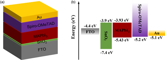
Fig. 1. (a) Device architecture of n-i-p MAPbI3 PSC for SCAPS simulation and (b) the corresponding energy level diagram.
Download figure:
Standard image High-resolution imageTable I. Basic parameters for each layer of the device.
| FTO | SnO2 | Absorber | Spiro | |
|---|---|---|---|---|
| Thickness (nm) | 600 | 50 | 250 | 250 |
| Bandgap (eV) | 3.50 | 3.50 | 1.55 | 2.91 |
| Electron affinity (eV) | 4 | 4 | 3.9 | 2.45 |
| Dielectric permittivity | 9 | 9 | 6.5 | 3 |
| CB effective density of states (cm−3) | 2.2 × 10¹⁸ | 2.2 × 10¹⁷ | 2.2 × 10¹⁸ | 2.2 × 10¹⁸ |
| VB effective density of states (cm−3) | 2.2 × 10¹⁸ | 2.2 × 10¹⁷ | 1.8 × 10¹⁹ | 2.2 × 10¹⁸ |
| Electron mobility (cm2 V−1 s−1) | 20 | 20 | 2 | 2 × 10⁻⁴ |
| Hole mobility (cm2 V−1 s−1) | 10 | 10 | 2 | 2 × 10⁻⁴ |
| Donor density (cm−3) | 2 × 10¹⁹ | 1 × 10¹⁸ | 1 × 10¹⁶ | 0 |
| Acceptor density (cm−3) | 0 | 0 | 0 | 2 × 10¹⁸ |
| Defect density (cm−3) | 1 × 10¹⁵ | 1 × 10¹⁵ | 1 × 10¹⁵ | 1 × 10¹⁵ |

Fig. 2. (a) Optical absorbance of MAPbI3 layer based on SCAPs simulation (b) J–V curve based on simulation and experimental result, respectively.
Download figure:
Standard image High-resolution image4. Results and discussion
4.1. Effect of changing defect density (Nt)
To investigate both bulk recombination and interface recombination, the Shockley Read Hall (SRH) model is utilized in this simulation. The trap-assisted SRH recombination is mainly acknowledged to be the dominant recombination mechanism in PSCs. 29) Owing to the undesired film quality such as poor crystallization and high surface defect in the absorber layer, the generated free electron and hole are of higher possibility to be captured and thus recombine in trap centers. This so-called trap-assisted SRH recombination has been widely used to assess the photoconversion loss in single absorber device, which can be described by Eq. (1). 30)

where the RSRH is the SRH recombination rate, n and p are the concentration of electron and hole, respectively, ni represents the intrinsic carrier density, τ represents the carrier lifetime, Ei and Et refer to conduction/VB and trapping energy level, respectively. It is evident that the SRH recombination rate is determined by the carrier lifetime of the perovskite layer. On behalf of interpreting the critical dependency of defect density for recombination, Eq. (2) is utilized to show the relation between carrier lifetime and defect density. 31)

where τ represents the carrier lifetime, σ is the carrier capture cross section, Nt is the defect density and vth refers to electron thermal velocity. According to the Eqs. (1) and (2), the defect density is inversely proportional to carrier lifetime owing to the constant parameters for σ and vth at RT. Therefore, the SRH recombination rate is exclusively dependent on the defect density. Figure 3(a) demonstrates the SRH recombination rate as a function of film depth with varied defect density for the absorber layer. Within the defect density of 1014 cm−3, the recombination rates are at a lower level in the range of absorber from 0.25 to 0.5 μm. As the defect density increases from 1014 to 1016 cm−3, the recombination rate rises significantly in the perovskite layer. Notably, in a high defect density of 1016 cm−3, a much steeper curve is observed for higher depth regions indicative to near the ETL side for the absorber layer. Since the sunlight illuminates the front of the device by the FTO side, there are masses of generated carriers accumulated in the first interface of ETL/absorber rather than the second absorber/HTL due to the excellent absorption of MAPbI3 perovskite. 32) The quantitative discrepancy for non-equilibrium carriers brings more trap states and recombination centers in the interface of ETL/absorber, and thus results in a rapidly increased recombination rate. As a result, Fig. 3(b) exhibits the J–V curves for varied defect densities from 1013 to 1017 cm−3. While the defect density increases from 1013 to 1015 cm−3, the device performance drops mainly attributed to the reduced Voc from 1.116 V to 0.993 V. Simultaneously, the Jsc nearly remains at the same level. However, when the defect density increases up to 1016 cm−3 or even higher, the observably severe recombination leads to the degradation both in Voc, Jsc and FF. Therefore, it is vital for PSCs to suppress the defect density within 1015 cm−3 in the absorber layer to obtain good PCE.
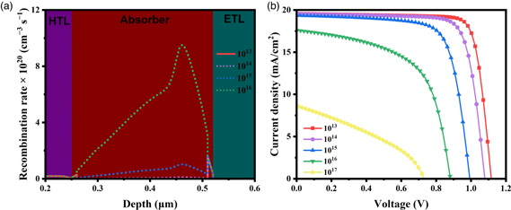
Fig. 3. (a) Recombination rate and (b) J–V curves based on different defect density in absorber layer.
Download figure:
Standard image High-resolution imageAs an excellent absorber material, MAPbI3 perovskite possesses a high diffusion length, which is beneficial for carrier extraction and even the absorption property in the near-spectral region. 33) Some researchers also reported a long diffusion length of over 1 μm in the nanostructured MAPbI3 perovskite. 34) Here we investigate the relation between diffusion length and bulk recombination to improve the device performance. Equation (3) describes the relation between carrier lifetime and diffusion length.

where D is the diffusion coefficient and is related to the carrier mobility. Therefore, the suppressed defect density leads to increased carrier lifetime and prolonged diffusion length, as summarized in Table II. Figure 4 demonstrates the variation in J–V characteristics as a function of the diffusion length. An impressive impact is observed mainly in Voc and FF owing to the higher diffusion length, attributed to suppressed defect density. Meanwhile, the effect on Jsc is very tiny while LD > 0.2 μm. Thus, the Voc improvement is dominant to affect PCE in this case. With the increasing diffusion length over 1.0 μm, the improvement of PCE is getting slower as well as Voc. According to the literature, the optimization for absorber quality such as additive doping and crystallization control is effective to improve the diffusion length of perovskite and obtain high performance. 35) Considering the actual experimental process in absorber deposition, the thickness of one-step MAPbI3 film is commonly within 500 nm. Under suppressed defect density of 5 × 1013 cm−3, the suitable carrier diffusion length for the subsequent simulation is assumed to be 720 nm with a carrier lifetime of 100 ns. Therefore, the better PCE of 17.86% is achieved with improved Voc of 1.097 V and FF of 79.8%, compared with the control device PCE of 15.68%. In addition, to avoid blocking the carrier extraction and transfer, the film thickness is preferable within 720 nm.
Table II. Summary of the photovoltaic parameters for varied diffusion length.
| N t (cm) | 1016 | 1015 | 1014 | 5 × 10¹³ | 1013 |
|---|---|---|---|---|---|
| τ (ns) | 0.5 | 5 | 50 | 100 | 500 |
| L D (μ m) | 0.051 | 0.16 | 0.51 | 0.72 | 1.6 |
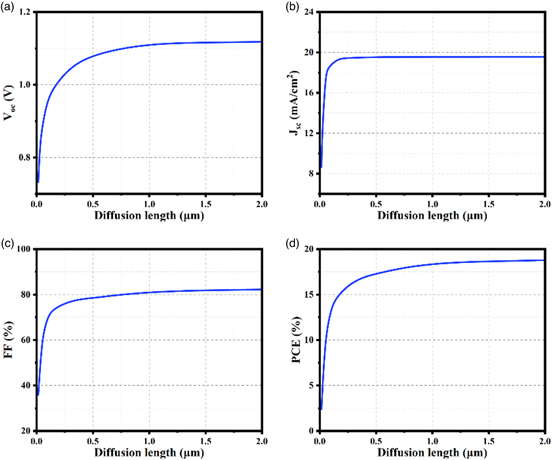
Fig. 4. J–V characteristics with varied carrier diffusion length: (a) PCE, (b) Voc, (c) Jsc and (d) FF.
Download figure:
Standard image High-resolution image4.2. Effect of absorber thickness
In Sect. 4.2, the effect of absorber thickness is compared and analyzed from 150 nm to 500 nm. Generally, with regard to the PSCs, the sufficient absorber thickness contributes to better device performance due to the preferable Jsc. 36) However, the excessively grown thickness may introduce problems of film morphology control and an increase of defect centers, which lead to severe recombination and Voc loss. 37) Figure 5 shows the J–V characteristics with varied MAPbI3 thickness from 150 nm to 500 nm to demonstrate the effect of absorber thickness, as summarized in Table III. It is clear the thicker absorber layer from 150 nm to 400 nm is beneficial for optical absorption and results in dramatically improved Jsc from 15.63 to 22.27 mA cm−2. Meanwhile, the Voc and FF have slight declines. Therefore, the PCE rises to 16.60% instead of 13.09%. On the contrary, since the thickness grows, the Voc reduces from 1.037 V to 0.992 V and FF reduces from 77.3% to 66.6% continuously because of the severe recombination. Additionally, the series resistance also has a potential impact on the declining performance, which we will discuss in detail hereinafter. Even though the absorption ability is getting better, the Jsc has gradually become saturated with sufficient thickness, inducing the PCE loss over the thickness of 400 nm. In summary, the desirable absorber thickness is around 400 nm to achieve optimized Jsc, proper Voc and FF, leading to superior device performance.
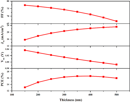
Fig. 5. The variations of J–V characteristics as a function of absorber thickness.
Download figure:
Standard image High-resolution imageTable III. Summary of the photovoltaic parameters for varied diffusion length.
| Thickness (nm) | PCE (%) | Voc (V) | Jsc (mA cm−2) | FF (%) |
|---|---|---|---|---|
| 150 | 13.09 | 1.037 | 15.63 | 77.3 |
| 200 | 14.66 | 1.029 | 17.82 | 76.5 |
| 250 | 15.68 | 1.022 | 19.45 | 75.5 |
| 300 | 16.30 | 1.015 | 20.67 | 74.4 |
| 350 | 16.58 | 1.009 | 21.59 | 72.9 |
| 400 | 16.60 | 1.003 | 22.27 | 71.2 |
4.3. Effect of ETL/HTL thickness
To investigate the effect of ETL/HTL thickness, the device performance is simulated with varied thickness of the transport layer, as shown in Fig. 6. As for ETL, we used colloid SnO2 precursor for deposition, which is interpreted in experimental Sect. 2. According to the literature, the thickness of SnO2 film is around 35 nm. 38) Thus, the varied thickness of ETL is set to be 20 to 100 nm in the simulation. Figure 6(a) shows the overall J–V characteristics, including FF, Jsc and Voc. The photovoltaic parameters almost remain constant since the thickness of ETL increases, which indicates an excellent carrier extraction capacity and defect-state tolerance. As a result, there is a negligible effect on device PCE by varying the ETL thickness. Conversely, the HTL exhibits a declined PCE from 15.75% to 15.55%, attributed to the decrease in FF from 75.9% to 74.9%. Meanwhile, other parameters like Voc and Jsc have no significant change, as shown in Fig. 6(b). The reason for the varied FF is that the Spiro-OMeTAD film with high resistivity leads to higher series resistance and poor conductivity which is harmful to charge transport and transfer, compared to the tiny impact from the relatively thin film of ETL with lower resistivity. 39,40) As an organic small molecule material, thin Spiro-OMeTAD film is also likely to suppress defects and achieves higher efficiency, as reported in several studies. 41,42) Therefore, the proper thickness of ETL and HTL is set to be 20 nm and 150 nm for the subsequent optimization.
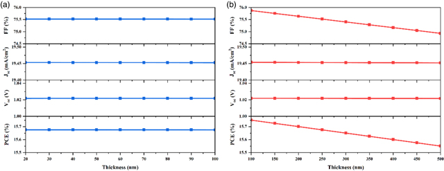
Fig. 6. The variations of J–V characteristics as a function of (a) ETL thickness and (b) HTL thickness.
Download figure:
Standard image High-resolution image4.4. Effect of interface recombination
After the assumption for both the absorber layer and transport layer, the interfaces between these layers are also investigated in Sect. 4.4. To analyze the effect of interface recombination, the IDLs with a thickness of 10 nm are simulated as ETL/perovskite and perovskite/HTL, respectively. Figure 7(a) presents the overall recombination from HTL-interface to ETL-interface based on the varied interface defect density from 1016, 1018 and 1020 cm−3, respectively. At the low interface defect density of 1016 cm−3, the dominant recombination is in the range of 0.15 μm to 0.57 μm, which refers to the majority of bulk region and the interface ETL/absorber, respectively. In particular, the recombination rate of the bulk region rises rapidly near the ETL side, indicative of the masses of carrier collection in interface ETL/absorber. Simultaneously, it shows a relatively minor peak for interface absorber/HTL. Figure 7(b) demonstrates the effect of interface defect density on device performance. With the interface defect density increased to 1018 cm−3 and even higher, the recombination rate of interface ETL/absorber emerges and becomes remarkably stronger. Therefore, the severely increased recombination restrains the electron extraction and collection efficiency in the FTO electrode, finally leading to heavy energy loss. The Voc shifts from 1.093 V to 1.036 V whereas the Jsc and FF almost remain the same. Thus, it leads to an efficiency discrepancy of around only 1% since the defect density increases by several orders of magnitude. Similarly, the peak of the interface absorber/HTL exhibits a relatively lower intensity and has a minor impact on device performance when the interface defect density is gradually increased, as shown in Fig. 7(c). The summary of J–V variation in Table IV shows that the interface ETL/absorber plays a critical role in interface recombination, which is harmful to the overall device parameters under high defect density (>1018 cm−3). One of the explanations could derive from the more generated carriers collected and accumulated at the front side during light illumination than at the backside. This high carrier density causes an increase in traps at the recombination centers. Generally, the surface for perovskite growth, which indicates SnO2 in this n-i-p structure, is of great significance for the formation of film morphology and interface defects. 43) Therefore, according to the J–V simulation, to get good carrier extraction and transfer, the defect density in interface ETL/absorber needs to be suppressed within 1017 cm−3.
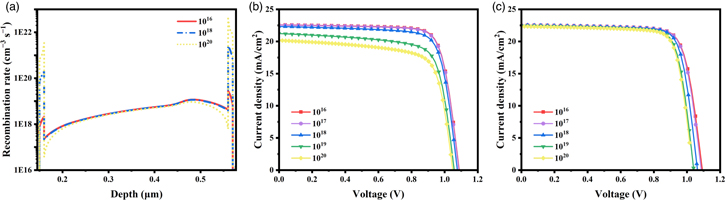
Fig. 7. (a) Recombination rate from HTL-side to ETL-side and J–V curves based on varied defect density in interfaces of (b) ETL/absorber and (c) absorber/HTL.
Download figure:
Standard image High-resolution imageTable IV. Summary of the photovoltaic parameters for varied defect density in ETL/absorber.
| Defect density (cm−3) | PCE (%) | Voc (V) | Jsc (mA cm−2) | FF (%) |
|---|---|---|---|---|
| 1016 | 20.17 | 1.088 | 22.58 | 78.6 |
| 1017 | 20.09 | 1.087 | 22.56 | 78.5 |
| 1018 | 19.43 | 1.077 | 22.33 | 77.3 |
| 1019 | 17.31 | 1.058 | 21.23 | 73.8 |
| 1020 | 16.00 | 1.049 | 20.17 | 72.4 |
4.5. Effect of doping concentration
In Sect. 4.5, we investigate the effect of doping concentration, which is also of great relevance for the bulk and interface recombination, as shown in Fig. 8. It has been reported that the doping concentration of MAPbI3 perovskite is a practical method, like cation doping, to improve the opto-electronic property. 44) Here we set a series of varied doping concentrations from 1013 to 1017 cm−3 to demonstrate the appropriate value for device performance. In the low concentration region within 1015 cm−3, the increased doping concentration obtains negligible change in recombination, as illustrated in Fig. 8(a). However, when it rises over 1015 cm−3, the recombination rate grows up by several orders of magnitude, especially approaching the side of interface ETL/absorber. Thus, it induces a larger amount of electrons accumulated in the interface ETL/absorber, especially for the concentration of 1017 cm−3, as shown in Fig. 8(b). While the doping concentration increases from 1015 cm−3 to 1016 cm−3, the electric field is reinforced and accelerates the separation of the photo-generated carriers, which contributes to a slightly enhanced Voc, as shown in Fig. 8(c). Nevertheless, the increasing bulk and interface recombination ascribed to changed doping concentration aggravates the device PCE with gradually decreased Jsc. Therefore, the reasonable doping concentration of perovskite should be assumed to be 1015 cm−3.
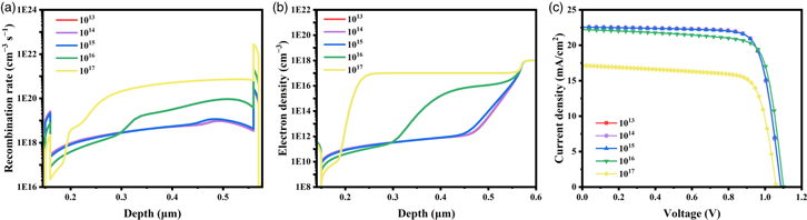
Fig. 8. (a) Recombination rate, (b) Electron density from HTL-side to ETL-side and (c) J–V curves based on varied doping concentration for perovskite layer.
Download figure:
Standard image High-resolution image4.6. Effect of series and shunt resistance
The effect of series resistance (Rs) is generally ascribed to the ohmic loss from bulk resistance and the electrode contact, especially at the interface contact of metal/semiconductor. 45) Basically, the origin of the shunt resistance (Rshunt) is from the leakage current, owing to the heavy defect states in the interface. 28) In PSCs, the introduced Rs commonly induces a severe energy loss compared to Rshunt. Therefore, here we evaluate the device performance with the varied Rs and Rshunt. 46) Figs. 9(a) and 9(b) depict the relations between device performance and Rs, in which the increased Rs aggravates the efficiency from 20.55% to 18.26%, mainly attributed to the accordingly declined FF from 80.3% to 71.4%. The photovoltaic parameters are summarized in Table V. The impact of the increased Rs can be approximately interpreted by Eq. (4), which is dependent synergistically on the internal absorber resistance and the contribution from electrodes. 47)

where b is absorber thickness, L is substrate length, and ρ and ρs refer to the resistivity of the absorber layer and FTO sheet resistance, respectively. On account of the constant effect from the electrode material, we ought to control the perovskite thickness because of the contribution for increased Rs, even thicker film will lead to higher Jsc. Meanwhile, the effect on device performance is slightly enhanced with highly increased Rshunt, as shown in Fig. 9(c). As a result, the PCE gradually improved as well as FF with reduced Rs and increased Rshunt for our simulation structure. Therefore, the optimized device requires the Rs within 1 Ω and Rshunt over 3000 Ω to get better FF.
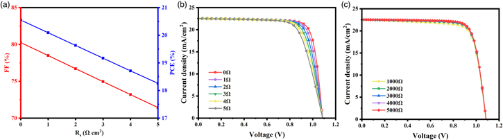
Fig. 9. (a) The variation of FF and PCE as a function of Rs. (b) J–V curves based on the varied Rs and (c) Rshunt.
Download figure:
Standard image High-resolution imageTable V. Summary of the photovoltaic parameters for varied Rs.
| Rshunt (Ω) | PCE (%) | Voc (V) | Jsc (mA cm−2) | FF (%) |
|---|---|---|---|---|
| 0 | 20.55 | 1.087 | 22.57 | 80.3 |
| 1 | 20.09 | 1.087 | 22.56 | 78.5 |
| 2 | 19.63 | 1.087 | 22.55 | 76.7 |
| 3 | 19.17 | 1.087 | 22.54 | 74.9 |
| 4 | 18.71 | 1.087 | 22.53 | 73.2 |
| 5 | 18.26 | 1.087 | 22.52 | 71.4 |
4.7. Optimized device performance
According to the modification and improvement above, including the suitably increased absorber layer thickness of 400 nm, thinner carrier transport layer thicknesses of 20 nm for ETL and 150 nm for HTL, suppressed defect density of 5 × 1013 cm−3 for absorber and 1017 cm−3 for interfaces, a well-controlled doping concentration of 1015 cm−3, Rs within 1 Ω and Rshunt over 3000 Ω, we reconstruct the device structure and obtain improved device performance. Importantly, the thicker absorber thickness provides sufficient optical absorption, leading to higher Jsc. Meanwhile, the suppressed bulk and interface recombination by suppressed defect density is the key point to achieving high Voc and PCE. As a result, Fig. 10 shows the optimized device achieves improved J–V characteristics with Voc of 1.087 V, Jsc of 22.56 mA cm−2, FF of 78.5%, and an encouraging PCE of 20.09%, compared to the control device with Voc of 1.022 V, Jsc of 19.45 mA cm−2, FF of 75.52% and PCE of 15.68%.

Fig. 10. The optimization result for J–V curves.
Download figure:
Standard image High-resolution image
5. Conclusions
In conclusion, our work has presented a dramatic improvement for device optimization on n-i-p structure PSCs via SCAPS-1D. Compared with our experimental result, the initial simulation for the control device is well-matched and exhibits distinct Voc loss and Jsc deficiency. It was found these poor performances could be attributed to the improper device structure and severe defects in bulk and interfaces. With the modification and improvement of various basic properties, the best simulation result is achieved with superb Voc, Jsc and FF, leading to encouraging PCE over 20% for pure-MAPbI3 PSCs. These optimizations unveil the critical role of defect suppression and provide a simple method to improve device performance on n-i-p MAPbI3 PSCs. For the purpose of realizing the S-Q limit of over 30%, further effort and design are required in optically corrected radiative loss and high-quality film which will avoid ohmic loss and defect-induced recombination.
Acknowledgments
This work is financially supported by the National Nature Science Foundation of China No. 62274065 and the Program of China Scholarships Council (No. 202106050022).