
Abstract
ZnS and CdZnS (a mixed crystal phase of ZnS and CdS) were formed using the open-air CVD method. Cadmium diethyldithiocarbamate (C10H20CdN2S4) and zinc diethyldithiocarbamate (C10H20ZnN2S4) were used as the source materials for CdS and ZnS, respectively. By changing the ratio of source materials, it was found that the bandgap and the lattice constant of the CdZnS film were continuously changing without a miscibility gap. Furthermore, the bandgap of the obtained ZnS films was less than the reported bandgap of ZnS (3.68 eV) due to incorporation of oxygen. X-ray diffraction analysis revealed that the increase of Zn in CdZnS film generated a crystalline disorder. When the substrate temperature was changed from 421 °C to 464 °C, the deposition rate increased fourfold for the CdS and ZnS films. The impact of substrate temperature on the bandgap and lattice constant was found to be less pronounced.
Export citation and abstract BibTeX RIS
1. Introduction
Cadmium sulfide (CdS) has been used as a buffer layer in various types of solar cells, including CuInx
Ga1−x
Se2 (CIGS), CdTe, Cu2ZnSnS4 (CZTS), and Cu2SnS3 (CTS) solar cells.
1–15) However, there are some issues with the CdS buffer layer. The first issue is that the buffer layer absorbs incident light in the short wavelength region (less than 512 nm) due to the relatively narrow bandgap of CdS (Eg = 2.42 eV).
16) The second issue is the negative offset between the conduction band edge of the light absorption layer and that of the buffer layer. When the conduction band edge of the light absorption layer is higher or lower than that of the buffer layer, the offset  is negative or positive, respectively. The positive
  is often referred to as a "spike" and the negative one as a "cliff." The negative
  causes a serious drop in the short-circuit current Jsc and open-circuit voltage Voc,
17) and the optimum cell performance is obtained when
causes a serious drop in the short-circuit current Jsc and open-circuit voltage Voc,
17) and the optimum cell performance is obtained when  becomes slightly (<0.3 eV) positive.
18,19) For example, in the case of CdTe solar cell, since the electron affinity of CdS is about 4.50 eV
20) and that of CdTe is about 4.28 eV,
20)
becomes slightly (<0.3 eV) positive.
18,19) For example, in the case of CdTe solar cell, since the electron affinity of CdS is about 4.50 eV
20) and that of CdTe is about 4.28 eV,
20)
 is negative
20,21) and not the optimum value for a solar cell. In particular, this optimization becomes more important in the case of wide-bandgap top cell in a multi-junction solar cell.
is negative
20,21) and not the optimum value for a solar cell. In particular, this optimization becomes more important in the case of wide-bandgap top cell in a multi-junction solar cell.
Since zinc sulfide (ZnS) has a wide bandgap of 3.68 eV
16) compared to CdS, a buffer layer composed of ZnS or CdZnS (a mixed crystal phase of ZnS and CdS) can reduce the absorption of short wavelength light. Furthermore, because of the property that the electron affinity of CdZnS ranges from 4.02 to 4.50 eV,
22,23) the CdZnS can be considered a promising material for  optimization. For example, in the case of the CdTe solar cell, the use of CdZnS as a buffer layer can make the
  slightly positive.
A successful case that the use of CdZnS improved the cell performance is found in the CIGS solar cell. Bhattacharya and his colleagues 24) demonstrated that using CdZnS instead of CdS as the buffer layer in CIGS solar cell increased the short-wavelength current density (Jsc) by 2 mA cm−2. This improvement resulted from the advantage that CdZnS has wide band gap. As a result, they obtained conversion efficiency of 19.52%. 24)
However, in this experiment, the CdZnS buffer layer was formed using the chemical bath deposition (CBD) method. Although the CBD method is a reliable process suitable for mass production, it has some limitations. For instance, the film composition may become non-homogeneous along the thickness due to the lower solubility of ZnS compared to that of CdS. 25,26) This issue makes it difficult to continuously control the ratio between Cd and Zn in CdZnS using the CBD method, even though this control is necessary for further optimization of the buffer layer. 22,23,27)
Various methods other than the CBD method such as vacuum evaporation, 28) photochemical deposition, 29) metal organic CVD (MOCVD), 30) successive ionic layer absorption and reaction, 31,32) ink-based method, 25) RF magnetron sputtering 33) and the use of CdS/ZnS hybrid layer 26,34) were examined for fabricating CdZnS. In principle, continuous control of the components in CdZnS can be achieved through the application of vacuum evaporation, MOCVD, photochemical deposition and RF magnetron sputtering. However, these methods are not suitable for mass production. Although the other methods described above are suitable for mass production, the control window of Cd and Zn in CdZnS is limited 25) or the control itself has not been mentioned in the literature. Thus, there are no reports that mention a method which enables both continuous control of the components in CdZnS and mass productivity.
We formed ZnS and CdZnS buffer layers by using the open-air CVD method. This method has been used previously to form CdS buffer layers for CdTe solar cells. 6,8–12) In this method, a ZnS or CdZnS film is created from gas sublimated from solid gas source. Since the forming process of the ZnS or CdZnS film does not involve water, this method avoids the problem caused by the difference in solubility between ZnS and CdS. Additionally, the composition of the sublimated gas can be adjusted by controlling the composition of the solid gas source, enabling continuous control of Cd-to-Zn ratio in CdZnS. Furthermore, the open-air CVD method is suitable for mass production, since it does not require waste liquid treatment and allows for the creation of a buffer layer at a much lower cost compared to the CBD method.
In the open-air CVD method, solid source materials of CdS and ZnS are mixed in advance to produce the source gas for the formation of CdZnS film. In this work, several CdZnS films were fabricated with variations in the composition of the source material. The dependence of the optical and structural properties of CdZnS films on the composition ratio was investigated, and it was demonstrated that the optical and structural properties of CdZnS can be continuously varied depending on the composition of the source material.
2. Experimental methods
Figure 1 illustrates schematic diagram of the open-air CVD method. Powdered cadmium diethyldithiocarbamate (C10H20CdN2S4) and powdered zinc diethyldithiocarbamate (C10H20ZnN2S4) were used as the source materials for CdS and ZnS, respectively. They were mixed in a mortar with the ratio R varied from 0% to 100%, where R is the ratio of the weight of C10H20CdN2S4 (the source material of CdS) to the weight of the total mixed source material. The mixed source material was dispersed in an organic solvent (propylene glycol) to form a paste, which was then printed on the glass substrate (Corning EAGLE XG). We define the glass substrate coated with this paste "source glass substrate." To heat the mixed source material to sublimation temperature, we placed the source glass substrate on the heater 1 [see Fig. 1] at 464 °C. We used another glass substrate, specifically Corning EAGLE XG, as the "target glass substrate." This substrate was placed on the heater 2 (see Fig. 1), which allowed us to control its temperature (Ts) within the range of 421 °C–464 °C. Next, we installed the already heated source glass substrate with a spacing of 0.7 mm, ensuring that the source material faced the film-growing surface of the target glass substrate. By exposing the target glass substrate to the sublimate from the source material, CdZnS film was deposited on the target glass substrate. Deposition time was controlled in the range from 180 to 360 s, depending on the target thickness of the film and deposition rate. By separating the source glass substrate from the target glass substrate, deposition process stopped.
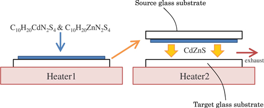
Fig. 1. Schematic diagram of the open-air CVD method.
Download figure:
Standard image High-resolution imageX-ray diffraction (XRD) analysis was conducted on CdZnS films to evaluate their lattice constant and crystallinity. The transmittance spectra of the films were also measured. From absorption edge of the transmittance spectrum, the optical band gap Eg was calculated using Tauc's theory. Film thickness was determined using two methods and crosschecked. One method involved calculating the period of interference fringe in the transmittance spectrum, while the other was the step measuring method. The CdZnS film was also subjected to cross- sectional observation and cross-sectional element analysis using transmission electron microscope (TEM) and TEM Energy dispersive X-ray spectroscopy (TEM-EDS), respectively.
3. Results and discussion
3.1. Dependence of optical and structural properties of CdZnS films on the weight ratio of source materials
It is essential to investigate the optical properties of CdZnS films for their potential use as an alternative buffer layer in thin-film solar cells. Several films were fabricated with the weight ratio R varied from 0% to 100%, where R represented the weight ratio of C10H20CdN2S4 (source material of CdS) to the total mixed source material. An R value of 100% indicated that the total source material consisted only of CdS, while an R value of 0% indicated that it consisted only of ZnS. In this experiment, all films were deposited at a temperature of Ts = 451 °C. The optical transmission spectra of the CdZnS films for various R values were recorded as a function of wavelength in the range of 300–600 nm, as shown in Fig. 2(a). The thicknesses of the films were 1240 nm, 1280 nm, 1090 nm, 312 nm, and 552 nm for R = 100%, R = 67%, R = 50%, R = 33%, R = 0% films, respectively. A gradual shift of the absorption edge of the transmittance spectrum towards shorter wavelengths was observed as R decreased. The optical bandgap Eg of the films can be determined from the absorption edge using Tauc's relation. Figure 2(b) illustrates the experimentally observed values of (αhν)2 plotted against hν, where α is absorption coefficient of light. To determine Eg, we extrapolated the linear portion of the curve to (αhν)2 = 0. By varying the ratio R from 0% (ZnS) to 100% (CdS), we observed a continuous change in Eg from 3.14 to 2.43 eV, as shown in Fig. 2(c).
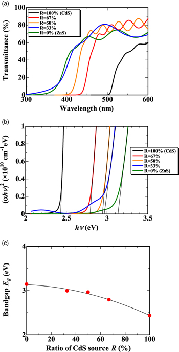
Fig. 2. (a) Optical transmission spectra of CdZnS films for various R. (b) Experimentally observed values of (αhν)2 plotted against hν. Red circle denotes the presence of defect level. (c) Dependence of bandgap Eg on the ratio R. The fitting curve in the figure is a polynomial approximation of the experimental data.
Download figure:
Standard image High-resolution imageAlthough the Eg expands as the ratio R is reduced, the Eg value of the R = 0% (ZnS) film (i.e. 3.14 eV) does not reach the Eg value of pure ZnS mentioned in literature (i.e. 3.68 eV). 16) The unexpected smaller Eg of the R = 0% film may be attributed to the incorporation of oxygen, since it is known that the bandgap narrows when oxygen is incorporated into the ZnS film. 35,36) A literature 35) describes that the bandgap can narrow to a minimum value of 2.6 eV by oxygen incorporation, and that the maximum narrowing width can reach up to 1.1 eV. In the open-air CVD method, the deposition process is performed in the air, which can lead to the oxygen incorporation in the film. TEM-EDS analysis revealed that the R = 0% film formed using the open-air CVD method contained approximately at 6% of oxygen.
TEM-EDS analysis showed that the R = 100% CdS film contained at 3% oxygen. If oxygen incorporation affects the Eg of an R = 0% film, then the Eg of an R = 100% film should also be affected similarly. However, the experimental value of Eg (i.e. 2.43 eV) in the R = 100% (CdS) film is almost identical to the literature value of Eg of pure CdS (i.e. 2.42 eV). 16) The fact that the Eg of the R = 100% film does not narrow as much as the Eg of the R = 0% film does is possibly explained by the fact that the bandgap of CdS is insensitive to the oxygen incorporation. It is known even in the case of pure CdO (where all the sulfur is replaced by oxygen) the direct bandgap is reported to be 2.35 eV in Ref. 37, 2.45 eV in Ref. 38, 2.4~2.42 eV in Ref. 39 and 2.4 eV in Ref. 40. Therefore, the difference in bandgap between pure CdO and pure CdS is at most 0.07 eV. This difference is smaller than the maximum bandgap narrowing width observed in ZnS (1.1 eV), as mentioned in the previous paragraph. This indicates that the bandgap narrowing width in CdS due to the oxygen incorporation is much smaller than that in ZnS.
XRD spectra were derived as shown in Fig. 3(a). The peak at 26.6 deg in the spectrum of R = 100% (CdS) and the peak at 29.2 deg in the spectrum of R = 0% (ZnS) are considered to be caused by the (111) crystalline planes of the sphalerite structure of CdS (JCPDS data card No. #89-0440) and (111) crystalline planes of the sphalerite structure of ZnS (JCPDS data card No. #71-5976) respectively. No peaks indicating a wurtzite structure, such as (101) or (100) crystalline planes of CdS (JCPDS data card No. #41-1049) and (010) or (011) crystalline planes of ZnS (JCPDS data card No. #36-1450) were observed in the spectra.

Fig. 3. (a) XRD spectra as R was varied from 0% to 100%. (b) Detailed XRD spectra around the peak corresponding to (111) crystalline planes (Normalized). (c) Dependence of lattice constant on the ratio R. The fitting curve in the figure is a polynomial approximation of the experimental data.
Download figure:
Standard image High-resolution imageThe detailed XRD spectra are illustrated in Fig. 3(b). It was observed that an increase in the ratio R from 0% to 100% caused the peak corresponding to the (111) crystalline planes to shift from 29.2 to 26.6 deg. Assuming that the crystal structure is a sphalerite structure, the lattice constants a were plotted as a function of the ratio R in Fig. 3(c). When the ratio R was varied from 0% to 100%, the lattice constant a continuously changed from 0.532 to 0.581 nm without a miscibility gap. From Fig. 3(c), it can be observed that the change in lattice constants for 0 ≦ R ≦ 0.5 is less pronounced compared to that for 0.5 ≦ R ≦ 1.0. This suggests a nonlinear relationship between lattice constant and R.
One reason of the nonlinear dependence would be that the ratio of ingredients composing sublimation gas does not change linearly with R. It is known that the mp (181 °C 41)) of C10H20ZnN2S4 (solid source of ZnS) is lower than that (255 °C 42)) of C10H20CdN2S4 (solid source of CdS), indicating that vapor pressure of the former is higher than that of the latter. Even if same amount of C10H20ZnN2S4 as C10H20CdN2S4 is contained in the mixed source material, the concentration of sublimated gas from the former is larger than that from the latter because of the higher vapor pressure of the former, which provides growing surface of CdZnS with more Zn than Cd. Namely, the ratio R does not control the concentration of Zn or Cd on the growing surface linearly, which leads to nonlinear scaling of the ratio of Cd or Zn in the CdZnS film against R.
It is known that the literature value of the lattice constant a for pure ZnS and that for pure CdS are 0.541 nm 43–45) and 0.583 nm, 46) respectively. We have compared these values with the results of our experiment. The lattice constant of the R = 100% film (0.581 nm) is smaller than that of pure CdS (0.583 nm) by 0.002 nm, and the lattice constant of the R = 0% film (0.532 nm) is smaller than that of pure ZnS (0.541 nm) by 0.008 nm. For both R = 100% and R = 0% films, the reduction of the lattice constants from those of the pure CdS and that of the pure ZnS was observed, however the reduction width in R = 0% film was more prominent compared to that in R = 100% film. It is well known that the bond distance of Zn–O 47) is smaller than the bond distance of Zn–S, due to smaller ion radius of oxygen compared to that of sulfur. Therefore, we can possibly explain the experimental finding that the lattice constant of the R = 0% film is smaller than that of pure ZnS by hypothesizing that some of the Zn–S bonds in the R = 0% film are replaced by Zn–O bonds.
The line width, expressed as the FWHM, of 29.2 deg peak of R = 0% film (ZnS) was evaluated to be 0.60 deg, while that of the 26.6 deg peak of the R = 100% (CdS) film was 0.38 deg. The FWHM in the former is larger than that in the latter, suggesting that the crystalline order in the R = 0% film is more degraded compared to that in R = 100% film. We cannot clarify the cause of this degradation. However, when a part of the sulfur in CdZnS is replaced by oxygen, this replacement can cause a distortion of crystalline order, since the bond distance between zinc (cadmium) and oxygen is smaller than the bond distance between zinc (cadmium) and sulfur. In order to analyze the correlation between oxygen and crystalline order systematically, we are planning a film deposition experiments in an atmosphere with controlled oxygen concentration.
To confirm the presence of crystalline structure in the film, we conducted TEM analysis. Figure 4 shows the cross-sectional images of the R = 100% (CdS) film and the R = 0% (ZnS) film, respectively. In these images, (a) and (c) represent the macroscopic view of the cross-section, while (b) and (d) show the microscopic view. Columnar growth of crystals was observed for both the R = 100% film and the R = 0% film from (a) and (c). Additionally, a lattice image was clearly observed in the column from (b) and (d), suggesting that the columns in both films contain perfect crystalline components.
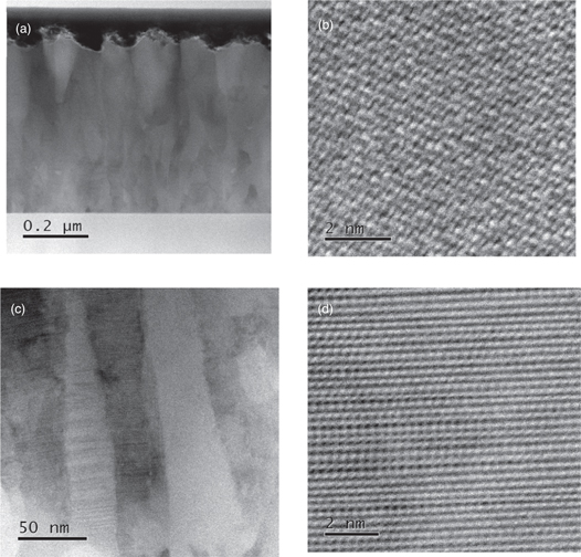
Fig. 4. (a) and (b) are cross sectional image of R=100% (CdS) film, where (a) is a macroscopic view and (b) is a microscopic view. (c) and (d) are cross sectional image of R = 0% (ZnS) film, where (c) is a macroscopic view and (d) is a microscopic view.
Download figure:
Standard image High-resolution image3.2. Dependence of optical and structural properties of CdZnS films on the substrate temperature
Next, we investigated the dependence of the optical and structural properties of CdZnS films on the substrate temperature. More than ten films were prepared with both the substrate temperature Ts and the ratio R varied, where Ts was in the range of 403 °C–464 °C. The Arrhenius plot of the deposition rates of these films is shown in Fig. 5. The deposition rate of films with Ts = 464 °C was four times larger than that of films with Ts = 421 °C for both the R = 100% (CdS) and R = 0% (ZnS) cases. The activation energy derived from the Arrhenius plot was 1.28 eV for R = 100% case and 1.23 eV for R = 0% case, respectively. Thus, a strong dependence of the deposition rate on Ts was observed, which suggests that the reaction on the target glass substrate surface rate-controls the growth of CdZnS films. As the data of the R = 50% film is scattered in the vicinity of the data of the R = 0% film, the deposition rate and the activation energy for the R = 50% film are considered to be close to those of the R = 0% film.
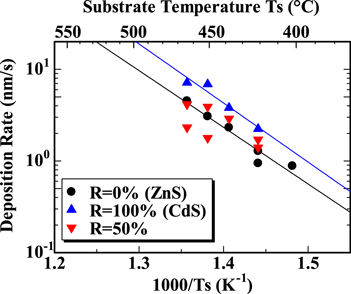
Fig. 5. Arrhenius plot of deposition rates.
Download figure:
Standard image High-resolution imageThree datasets containing three sample each were extracted from the data base. In each dataset, three samples were created at the same Ts but with different R ratios (0%, 50% and 100%). Ts was different for each dataset (421 °C, 451 °C and 464 °C). The thicknesses of the films in these datasets are scattered in the range from 335 to 1290 nm.
The bandgap Eg, estimated from the transmission spectra of the three data sets, was plotted as a function of Ts, as shown in Fig. 6. As Ts increased from 421 °C to 464 °C, Eg remained constant for R = 100% (CdS), R = 50%, and R = 0% (ZnS) films.
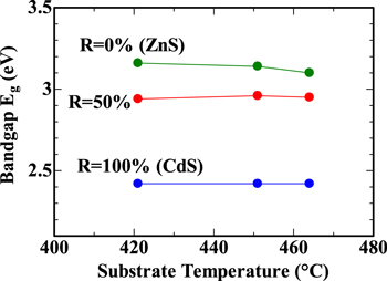
Fig. 6. Bandgap Eg plotted as a function of substrate temperature Ts.
Download figure:
Standard image High-resolution imageThe dependence of XRD spectra on Ts was studied. The lattice constants were estimated from the peak angle of XRD spectra and were plotted as a function of Ts (Fig. 7). The lattice constants for R = 0%, 50%, and 100% remained almost constant despite the change in Ts.

Fig. 7. Lattice constant plotted as a function of substrate temperature Ts.
Download figure:
Standard image High-resolution imageAs Ts is increased, the FWHM of the peak corresponding to the (111) crystalline planes decreased, as shown in Fig. 8, indicating an improvement in the crystalline order of the CdZnS film. One of the reasons for this improvement can be the enhanced migration of the precursor on the growing surface of the CdZnS film.
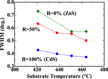
Fig. 8. FWHM of the peak corresponding to (111) crystalline planes plotted as a function of substrate temperature Ts.
Download figure:
Standard image High-resolution imageAlthough the impact of bandgap and lattice constant on Ts is less pronounced, two clear changes due to the variation in Ts are seen in the XRD spectrum of the R = 0% (ZnS) film. One change is related to the count rate in the XRD peak. Figure 9(a) shows a comparison of the XRD spectrum of the Ts = 451 °C film with that of the Ts = 421 °C film. Despite the fact that the thickness of the two films is similar (550 nm and 460 nm), the intensity of the peak height for the former is approximately seven times greater than that of the latter. This result suggests an increase in the volume fraction of the crystal phase as well as an increase in crystalline order due to the increase in Ts.

Fig. 9. (a) Comparison of the spectrum of the R = 0% film deposited in Ts = 451 °C with that deposited in Ts = 421 °C. (b) enlarged image of (a).
Download figure:
Standard image High-resolution image
The other change relates to the crystalline structure. Figure 9(b) illustrates an enlarged image of Fig. 9(a). The spectrum of the film deposited at Ts = 451 °C consists of only one peak at 29.1 deg, while the spectrum of the film deposited at Ts = 421 °C apparently contains three peaks at 27.6 deg. (denoted by A), 29.2 deg (denoted by B) and 31.0 deg (denoted by C). The peak at 29.1 deg. in the Ts = 451 °C film is identified as the (111) crystalline plane of the sphalerite structure of ZnS. On the other hand, the two peaks at 27.6 deg and 31.0 deg in the Ts = 421 °C film are identified as the (010) and (011) crystalline planes of the wurtzite structure of ZnS, respectively (JCPDS data card No. #36-1450). Since the peak at 29.2 deg (denoted by B) in the Ts = 421 °C film could be formed by merging the peak corresponding to the (111) crystalline plane of the sphalerite structure with the peak corresponding to the (002) crystalline plane of the wurtzite structure of ZnS, the crystalline phase in the Ts = 421 °C film might be a mixed phase of sphalerite crystal and wurtzite crystal. However, it is plausible that the reduction of Ts brings about a change in the crystalline structure from sphalerite to wurtzite at least in a part of the crystal.
4. Conclusions
ZnS and CdZnS were formed by the open-air CVD method. The open-air CVD method allows for continuous control of film composition, which is difficult with the conventional CBD method. We aimed to achieve "continuous control" of film composition in CdZnS. Cadmium diethyldithiocarbamate (C10H20CdN2S4) and zinc diethyldithiocarbamate (C10H20ZnN2S4) were used as the source materials for CdS and ZnS, respectively.
By changing the ratio R of the C10H20CdN2S4 to the total mixed source material from 0% (ZnS) to 100% (CdS), we found that the bandgap and the lattice constant of the CdZnS film were continuously changed without a miscibility gap, ranging from 3.14 to 2.43 eV and from 0.532 to 0.581 nm, respectively. As a conclusion, it turns out that the optical and structural properties can be "continuously" controlled by varying the ratio R in the open-air CVD method. Analysis of the FWHM of the XRD peak and the absorption edge of the transmittance spectrum revealed that the incorporation of Zn into the CdS film generates crystalline disorder and increases the defect level at the band edge.
When the substrate temperature was increased from 421 °C to 464 °C, the deposition rate increased fourfold for both the R = 100% (CdS) film and the R = 0% (ZnS) film. The effect of substrate temperature on the bandgap and lattice constant was found to be less pronounced.
Acknowledgments
This work is financially supported by a collaborative research grant between Nagaoka University of Technology (NUT) and the National Institute of Technology (NIT).