
Abstract
Cu2SnS3 (CTS), obtained by depositing Au on an Sn/Cu metal stacked precursor fabricated by electron beam deposition and sulfurization, was investigated. In thin films obtained by sulfurization at 560 °C of the precursor with SLG/Mo/Sn/Cu/Au/NaF structures fabricated on Soda lime glass substrates containing alkali metals, a significant increase in the CTS grain size was observed in the Au deposition thickness range of 5–25 nm. By contrast, no crystal growth was observed in thin films with a precursor without an NaF layer fabricated using alkali-free glass (EAGLE XG), regardless of the thickness of the Au-deposited film. Therefore, appropriate amounts of Au and Na promote the crystal growth of CTS. In addition, at the sulfurization temperature of 570 °C, the crystal grains were larger than those of the thin film fabricated at 560 °C. In the fabricated CTS thin-film solar cells, with a sulfurization temperature of 570 °C and an Au deposition thickness of 10 nm, open circuit voltage of 0.261 V, short circuit current density of 25.4 mA cm−2, fill factor of 0.425, and a power conversion efficiency of 2.82% were obtained.
Export citation and abstract BibTeX RIS
1. Introduction
Recently, Cu(In,Ga)Se2 (CIGSe)-based thin-film solar cells, which are the leading chalcogenide-based thin-film solar cells, have achieved power conversion efficiency (PCE) exceeding 20%. 1) Kesterite-Cu2ZnSnS4 (CZTS) and Cu2ZnSn(S,Se)4 (CZTSSe), which are analogous to CIGSe, are relatively non-toxic to CIGSe and are composed of elements abundant in the Earth's crust, attracting attention as low-cost and less environmentally hazardous materials. However, the PCE in CZTS-based thin-film solar cells is approximately 10%, and that in CZTSSe is only approximately 13%. 2–4) One of the reasons for the sluggish PCE of CZTS and CZTSSe solar cells is the easy formation of defects derived from Cu and Zn. 5) Another concern is that CZTSSe, like CIGSe, contains Se, a toxic element. Therefore, we focused on Cu2SnS3 (CTS), a ternary chalcogenide. The structure of solar cells using CTS as a light-absorption layer was first reported by Kuku and Fakolujo. 6) CTS is a p-type semiconductor with a direct bandgap composed of versatile elements; it has a high optical absorption coefficient on the order of 104 cm−1 in the visible light region, which has proved promising as a light absorption layer in solar cells. 7,8) The highest reported PCE based on CTS is 5.2%, with Ge alloying yielding a PCE of 6.7%. 9,10) Furthermore, the effect of Ag addition to CTS has also been reported, and improvement in photovoltaic parameters and crystal growth of CTS due to the slight solid solution of Ag have been found. 11–15) However, the reported PCE resulting from the effect of Ag addition to CTS is only 4.7%. 14) In contrast to the widely reported systems in which Ag is introduced into CIGSe and CZTSSe, 16–24) which are analogous to CTS, there are few reports on adding Ag to CTS. Therefore, it is necessary to examine the effects of adding elements other than Ag to improve the properties of CTS solar cells. Another candidate for adding elements to CTS is Au, which belongs to the same group as Cu and Ag. There have been no reports of the addition of Au to CTS solar cell devices; therefore, it is interesting to investigate its effect. In this study, CTS thin films were prepared by sulfurizing Au-deposited Sn/Cu metal stacked precursors, and the effect of Au deposition on CTS crystals and their photovoltaic characteristics in solar cell devices was investigated.
2. Experimental methods
Approximately 1 μm thick layer of Mo was deposited on soda lime glass (SLG) by DC sputtering using a 99.95% pure Mo target. Mo was deposited on an alkali-free substrate (EAGLE XG) using the same procedure. On the fabricated Mo back electrode, 340 nm of Sn (99.99% purity) and 260 nm of Cu (99.9999% purity) were deposited via electron beam deposition at a substrate heating temperature of 130 °C. Subsequently, Au (99.99% purity) with varying thicknesses was deposited on the precursor. All Au films were deposited by DC magnetron sputtering (JFC-1600 AUTO FINE COATER, JEOL) under an Ar atmosphere at a pressure of 10 Pa and a sputtering current of 20 mA for a specified time. The distance between the target and the sample was set at 40 mm. The thickness of the Au-deposited film was limited to 0–200 nm for the precursor fabricated on SLG and 0–15 nm for EAGLE XG. The fabricated SLG/Mo/Sn/Cu/Au (0–200 nm) precursor was deposited with 10 mg of NaF (99.0% purity) on a Mo boat using thermal evaporation. No NaF was deposited on the precursor of the EAGLE XG/Sn/Cu/Au (0–15 nm) structure to fabricate the Na-free samples. A schematic diagram of the sulfurization tube furnace is shown in Fig. 1. Regardless of the type of glass substrate, each precursor was placed in a quartz ampoule with 100 mg of S (99.999% purity), heated from RT to 560 °C in a tube furnace at a rate of 10 °C min−1 in an N2 atmosphere, and held at 560 °C for 2 h before being allowed to cool. The surface morphologies of the thin films obtained were characterized using a scanning electron microscope (SEM; JSM-6060LV, JEOL). We also measured the crystal structures of the obtained thin films using X-ray diffraction (XRD; Miniflex, Rigaku). Surface crystalline phase analysis was performed using Raman spectroscopy (RMP-510, JASCO) at an excitation wavelength of 532 nm.
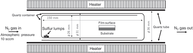
Fig. 1. Schematic diagram of a sulfurization tube furnace.
Download figure:
Standard image High-resolution imageTo investigate the sulfurization temperature of CTS fabricated via Au deposition, samples were prepared using the same process as that for 560 °C sulfurization, with the maximum temperature set at 570 °C for the SLG/Mo/Sn/Cu/Au (0–15 nm)/NaF precursors. The crystal structure of the obtained thin films was measured using XRD and Raman spectroscopy, and the surface morphology was evaluated using SEM. SLG/Mo/CTS thin films prepared by NaF deposition and sulfurization at 560 °C and 570 °C, respectively, were then deposited with an n-type buffer layer of CdS via chemical bath deposition and annealed at 200 °C for 30 min under atmospheric conditions. After that, ZnO:Al was fabricated as a window layer via RF sputtering, and Al grid electrodes were formed to fabricate the SLG/Mo/CTS/CdS/ZnO:Al/Al solar cell devices. After scribing to divide into multiple cells, aperture areas were measured with an optical microscope (STZ-168-TL-T2, SHIMADZU Excellence in Science). The measured aperture areas excluded from the Al grid electrode area were 0.17–0.30 cm2. The current density–voltage characteristics (J–V) of the fabricated solar cell devices were measured under 100 mW cm−2 irradiation at AM1.5, using a solar simulator (SX-UI500XQ, Ushio, and SML 250 J, Bunkoukeiki).
3. Results and discussion
3.1. Na dependence in CTS thin films prepared by depositing Au
First, the Na dependence of CTS fabricated by depositing Au on a precursor was investigated. The Na-added sample was obtained by sulfurizing the SLG/Mo/Sn/Cu/Au/NaF stacked precursors. The fabrication technique involving the deposition of NaF onto the precursor as an Na source has been employed in achieving the highest reported CTS PCE of 5.2%. 9) Na-free CTS thin films were fabricated using an alkali-free glass (EAGLE XG) substrate instead of SLG in a process without NaF deposition. Figure 2(a) shows the surface SEM image of a thin film of the SLG/Mo/Sn/Cu/Au (0–200 nm)/NaF precursor structure after sulfurization at a maximum temperature of 560 °C. The grain sizes of the samples fabricated with Au deposition thicknesses of 5–25 nm were significantly larger than those of the Au-free samples. However, grain size decreased when the thickness of the Au-deposited film exceeded 50 nm. These results suggest that adding a small amount of Au to CTS contributed to the growth of CTS crystals. Based on these results, the Au deposition thickness in the Na-free CTS thin films was set in the range of 5–15 nm, which is considered effective for CTS grain growth in CTS prepared with Na and the Au-free reference. Figure 2(b) shows the surface SEM image of a CTS thin film obtained by sulfurizing a precursor with an EAGLE XG/Mo/Sn/Cu/Au (0–15 nm) structure fabricated using alkali-free glass (EAGLE XG). Comparing the Au-free thin films under both conditions, grain growth was poor for the Na-free CTS films compared to the Na-added CTS thin films. Crystal growth due to NaF deposition and sulfurization of the precursor was consistent with previously reported results. 9,25,26) In addition, we reported that crystal growth was not observed in Na-free CTS fabricated on alkali-free substrates, as in Na-added thin films. 27) However, no significant crystal growth was observed in the Na-free thin films prepared by depositing 5–15 nm Au. This suggests that in systems with coexisting Au and Na, the crystal growth of CTS is induced by the appropriate thickness of the Au deposition. One possible mechanism for CTS crystal growth is the formation of low-melting compounds containing Au and Na. In the Au–Na system, it has been reported that a liquid phase occurs below 570 °C in the region where the Au content is low. 28) Consequently, crystal growth may be facilitated by the presence of an Au–Na liquid phase acting as a flux.
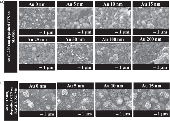
Fig. 2. Surface SEM images of thin films obtained by sulfurization of precursor with SLG/Mo/Sn/Cu/Au (0–200 nm)/NaF and EAGLE XG/Mo/Sn/Cu/Au (0–15 nm) structure.
Download figure:
Standard image High-resolution imageFigure 3(a) shows the XRD spectra of thin films prepared by adding Na. The powder diffraction file (PDF) was used to identify the crystalline phase, and the diffraction peaks were rearranged regarding the peak at 40.5° in Mo (PDF#00-042-1120). The diffraction peaks of the CTS phase were observed in all the thin films, but discriminating between the monoclinic (PDF# 01-070-6338) and cubic (PDF#00-089-2877) structures is not straightforward. Only the CTS phase was obtained for the Au-free thin films. The phases shown in • were not observed in the Au-free thin films but were commonly found in thin films obtained by Au deposition. The 34° phase was also observed in the XRD spectrum of the Au-free sample of the Na-free thin film shown in Fig. 3(b), suggesting that it is an impurity not caused by Au. As a breakdown of peaks other than CTS, peaks at 26°, 32°, and 38° were observed in thin films with Au deposition thicknesses of 5 nm or greater, in addition to peaks at 30° and 53° for films 10 nm or greater and peaks at 48° and 51° for films 25 nm or greater. These peaks appear with increasing Au deposition thickness and may belong to Au-containing compounds that do not correspond to the CTS phase or Au. In addition, elemental Au (PDF#00-004-0784) patterns were observed in the thin films with Au deposition thicknesses between 50 and 200 nm. The decrease in grain size observed in thin films with Au deposition thicknesses greater than 50 nm suggests that the residual elemental Au may inhibit the crystal growth of CTS. Figure 3(b) shows the XRD spectra of Na-free CTS thin films for each Au deposition thickness. As mentioned, a 34° peak was detected in the Na-free thin film, regardless of the addition of Au. The Au peak was not observed in the Na-added thin film until the Au deposition thickness reached 50 nm. In the Na-free condition, the Au peak was observed in the thin films with Au deposition thicknesses of 10–15 nm. In addition, the phases indicated by • observed in the Na-added thin film were not observed under Na-free conditions. The disappearance of these phases could indicate that the addition of Na did not form compounds containing Au and Na.
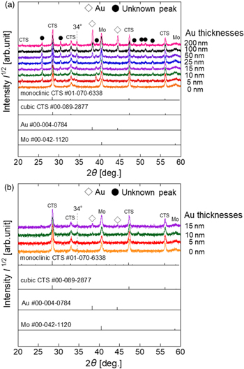
Fig. 3. XRD spectra of thin films obtained by sulfurizing (a) SLG/Mo/Sn/Cu/Au/NaF precursors with varying Au deposition thickness ranging from 0 to 200 nm and (b) EAGLE XG/Mo/Sn/Cu/Au precursors (without NaF layer) with Au deposition thickness varied from 0 to 15 nm.
Download figure:
Standard image High-resolution imageRaman spectroscopy was conducted for a detailed crystallographic analysis of the CTS phase. Figure 4(a) shows the results of the Raman spectroscopy of CTS thin films fabricated with various Au deposition thicknesses. The Raman spectra of the Au-free thin film showed peaks slightly shifted to higher wavenumbers from the 290 and 352 cm−1 peaks of the monoclinic structure. 29) This is a composite peak with cubic CTS with peaks at 303 cm−1 and 356 cm−1, suggesting that monoclinic and cubic structures coexist on the top surface of Au-free CTS. 30) By contrast, a single phase of monoclinic-CTS was obtained in the Au-added CTS thin film, irrespective of the thickness of the Au-deposited film. It has been reported that the cubic structure of CTS forms at approximately 500 °C and undergoes a phase transition to a monoclinic structure at approximately 575 °C. 31) The presence of the cubic phase leads to a decrease in the open-circuit voltage and short-circuit current density in CTS solar-cell devices. The Raman spectroscopy results suggest that adding Au to CTS may promote the phase transition to a monoclinic structure at low temperatures in CTS. Figure 4(b) shows the Raman spectra of CTS for each thickness of Au deposited in the Na-free state. A spectrum shift to the higher end of the monoclinic-CTS peak at 290 cm−1 was observed for all Au deposition thicknesses. These results indicate that adding Na and an appropriate amount of Au promoted the formation of CTS with a monoclinic structure and the growth of crystal grains.
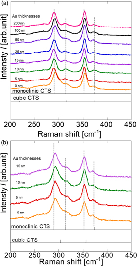
Fig. 4. Raman spectra of thin films obtained by sulfurizing (a) SLG/Mo/Sn/Cu/Au (0–200 nm)/NaF precursor films and (b) EAGLE XG/Mo/Sn/Cu/Au (0–15 nm) precursors.
Download figure:
Standard image High-resolution image3.2. Sulfurization temperature dependence of crystal growth of CTS thin films prepared by Au deposition and solar cell applications
Next, the temperature dependence of the sulfurization of SLG/Mo/Sn/Cu/Au (0–15 nm)/NaF was investigated. CTS thin films were prepared in the Au deposition thickness range of 0–15 nm by holding the films for 2 h at maximum sulfurization temperatures of 560 °C and 570 °C, respectively. The surface SEM images of the thin films obtained at each sulfurization temperature are shown in Fig. 5. Comparing the Au-free conditions, sulfurization at 570 °C increased the CTS grain size. In sulfurization at 570 °C, a significant increase in grain size was observed for all Au deposition thicknesses from 5 to 15 nm. Moreover, sulfurization at temperatures higher than 560 °C led to a further increase in grain size and voids, which were not observed in the 560 °C thin film.
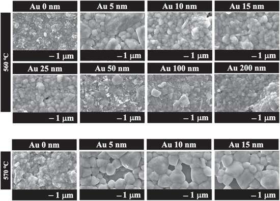
Fig. 5. Surface SEM images of thin films obtained by sulfurization of SLG/Mo/Sn/Cu/Au/NaF precursors prepared by setting the sulfurization temperature to 560 °C and 570 °C and varying the thickness of the Au deposited film.
Download figure:
Standard image High-resolution imageFigure 6 shows the XRD spectra of CTS thin films fabricated at a sulfurization temperature of 570 °C for each Au deposition thickness. The peaks at 26°, 30°, 32°, 38°, 48°, 51°, and 53° observed in thin films prepared with Au deposition were also observed in thin films with sulfurization at 560 °C with Na addition. Other peaks were detected at 29°, 43°, 44°, and 50°, which were not observed in the sample sulfurized at 560 °C. The detailed crystalline phase analysis in the obtained CTS was performed using Raman spectroscopy, as in the earlier experiments. Figure 7 shows the Raman spectra of CTS thin films fabricated by depositing Au (0–15 nm) at a sulfurization temperature of 570 °C. All CTS films fabricated at 570 °C were attributed to a single monoclinic phase, which was independent of Au deposition. The peak observed at 408 cm−1 is the MoS2 peak formed by the reaction of Mo from the back electrode with sulfur during sulfurization. 32)
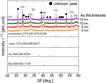
Fig. 6. XRD spectra of thin films of sulfurization at 570 °C at each Au deposition thickness.
Download figure:
Standard image High-resolution image
Fig. 7. Raman spectra for different thicknesses of Au deposition in CTS thin films obtained by sulfurization at 570 °C.
Download figure:
Standard image High-resolution imageFigure 8 shows the photovoltaic parameters of the solar cell devices fabricated using Au-deposited CTS thin films at 560 °C and 570 °C. For the thin films sulfurized at 560 °C, the open-circuit voltage (Voc), short-circuit current density (Jsc), and fill factor (FF) tended to improve in the Au deposition thickness range of 0–25 nm compared with the Au-free cells. By contrast, Voc and FF decreased with Au deposition thicknesses of 50 nm or greater. There was no significant change in Jsc with increasing Au deposition in the region above 50 nm, but Voc and FF decreased significantly from those of the Au-free sample at an Au deposition thickness of 200 nm. The sample sulfurized at 570 °C showed improved cell characteristics by adding Au. Voc remained unchanged regardless of the Au thickness, but Jsc and FF were significantly improved for all conditions from 5 to 15 nm Au thickness. This improvement in photovoltaic properties is thought to be due to the suppression of carrier recombination in the light-absorbing layer caused by the reduction in CTS grain boundaries due to Au- and Na-induced CTS crystal growth. The obtained Voc indicated that the p–n junctions have been successfully formed in the fabricated solar cells. Additionally, no segregated Au was observed in the surface SEM images. As a result, it is hypothesized that there is a minimal presence of elemental Au on the CTS surface. The best cell in the sample was obtained with Voc = 0.261 V, Jsc = 25.4 mA cm−2, FF = 0.425, and PCE = 2.82 at a sulfurization temperature of 570 °C and an Au deposition thickness of 10 nm.

Fig. 8. Photovoltaic parameters for each Au deposition thickness in solar cell devices fabricated with CTS thin films obtained by sulfurization at 560 °C and 570 °C. The open circles represent the measured values, and the closed circles represent their average.
Download figure:
Standard image High-resolution image
4. Conclusions
CTS thin films prepared by sulfurization of precursors with SLG/Mo/Sn/Cu/Au/NaF and EAGLE XG/Mo/Sn/Cu/Au structures at a maximum achievable temperature of 560 °C were investigated. SEM images of CTS samples fabricated using SLG substrates and NaF layers revealed enlarged CTS crystals in the range of 5–25 nm Au deposition thickness. In the CTS thin film with the EAGLE XG substrate and no NaF layer deposited, Au deposition did not induce crystal growth in the CTS thin film. This indicates that the combined contribution of Na and Au promotes CTS crystal growth. In the case of the SLG substrate with Au (5–15 nm) and NaF layers, CTS crystal growth was observed more significantly at a sulfurization temperature of 570 °C than at 560 °C. The XRD results showed many peaks indicating phases other than CTS in the thin films prepared by NaF and Au deposition, which were not observed in the thin films on EAGLE XG without NaF deposition. This suggests that compounds containing Au and Na may have been formed. The results of Raman spectroscopy show that the Au-free thin film contains a cubic phase at 560 °C sulfurization, even with NaF deposition; however, the phase transition to a monoclinic structure is enhanced by Na and Au. The best performance of the SLG/Mo/CTS/CdS/ZnO:Al/Al solar cell was obtained with a sulfurization temperature of 570 °C and an Au deposition thickness of 10 nm, Voc = 0.261 V, Jsc = 25.4 mA cm−2, FF = 0.425, and PCE = 2.82%, showing an improvement in photovoltaic characteristics compared to the Au-free cell.
Acknowledgments
We thank Mr. M. Yoneyama for conducting preliminary experiments. This work was partly supported by the Japan Society for the Promotion of Science KAKENHI (Grant No. JP19H02663).