
Abstract
We investigated the effect of the B2H6 plasma treatment on p-type hydrogenated amorphous silicon (p-a-Si:H) surfaces for high-performance silicon heterojunction (SHJ) solar cells. Secondary ion mass spectroscopy measurements revealed that the boron concentration at the p-a-Si:H surface is increased by employing the B2H6 plasma treatment. Furthermore, specific contact resistance is decreased by about one-third after the B2H6 plasma treatment. No degradation of passivation performance is induced by the B2H6 plasma treatment. The power conversion efficiency of the SHJ solar cells with the B2H6 plasma treatment is improved by the increase in fill factor (FF) due to decreased series resistance and increased shunt resistance. From numerical simulations, the upward band bending is enhanced at the heterointerface between transparent conductive oxide (TCO) and p-a-Si:H by the B2H6 plasma treatment, which is responsible for the improved FF owing to facilitated tunneling holes from c-Si to p-a-Si:H layers and the TCO/p-a-Si:H heterointerface.
Export citation and abstract BibTeX RIS
1. Introduction
The importance of photovoltaics is increasing since it is considered the primary power source for a decarbonized society. Among many varieties of solar cells, silicon heterojunction (SHJ) solar cells using hydrogenated amorphous Si (a-Si:H) exhibit an extremely high conversion efficiency exceeding 25%, 1–4) leading to high power generation by photovoltaics. The stack of a doped a-Si:H layer and an intrinsic a-Si:H (i-a-Si:H) layer is employed in conventional SHJ solar cells due to its high passivation performance against the c-Si surface. The excellent passivation performance results in a high open-circuit voltage (VOC) value, which is an attractive feature of SHJ solar cells. 5–7) Another feature of SHJ solar cells is the low-temperature coefficient of VOC compared to homojunction c-Si solar cells, which is advantageous for generating a higher power under practical operating conditions. 8,9) Therefore, SHJ can be expected to accelerate the utilization of photovoltaics and thus the realization of a decarbonized society.
The p-type a-Si:H (p-a-Si:H) is regarded as an issue that limits the performance of SHJ solar cells. Boron doped a-Si:H is commonly used as the p-a-Si:H for SHJ solar cells, and its typical conductivity is in the order of about 10−4 S cm−1. This requires transparent conductive oxide (TCO) films to collect the carriers into metal electrodes. Gogolin et al. reported that the largest resistive loss is caused by the carrier transport through the a-Si:H and across the TCO/a-Si:H interface. 10) In particular, larger contact resistance is originated not from TCO/n-a-Si:H/i-a-Si:H contact but from TCO/p-a-Si:H/i-a-Si:H contact. 10–12) Hence, the electrical contact properties at the TCO/p-a-Si:H interfaces are the bottleneck to achieving low resistive loss. Bivour et al. carried out a numerical analysis of the TCO/p-a-Si:H contact properties and revealed that better contact properties at the TCO/p-a-Si:H are accomplished by heavily doped p-a-Si:H. 13) In the numerical device simulation, defect formation depending on the doping variation of the p-a-Si:H layer is not taken into account. 13) However, in reality, degradation of passivation performance is often caused by depositing boron-doped a-Si:H. 14) De Wolf argued that the degraded passivation performance is attributed to Fermi energy-dependent Si–H bond rupture. 15,16) Based on this notion, B doping in a-Si:H tends to facilitate the destruction of Si–H bonds, leading to the degradation of passivation levels in SHJ solar cells. This suggests that lightly doped p-a-Si:H is beneficial to passivation performance. Thus, simultaneous attainment of good contact properties at the TCO/p-a-Si:H and a high level of passivation is challenging and crucial for high-performance SHJ solar cells.
In this study, we proposed a B2H6 plasma treatment on the surface of the p-a-Si:H layer to improve contact properties at the TCO/p-a-Si:H heterointerface. The B2H6 plasma treatment can create highly concentrated doping atoms in an extremely thin layer. Indeed, a heavily B-doped layer is employed in a-Si:H thin film solar cells and successfully enhances the conversion efficiency. 17,18) In SHJ solar cells, the B2H6 plasma treatment can suppress the doping level in the p-layer, while increasing the doping level at the p-a-Si:H surface. Hence, the contact properties of the TCO/p-a-Si:H heterointerface are expected to be improved without significant degradation of its passivation performance.
2. Methods
All depositions were performed on c-Si(100) substrates by a plasma-enhanced CVD (PECVD) system with a frequency of 27.12 MHz (ULVAC Inc., CME-200J). SiH4, H2, PH3, and B2H6 were used as source gases. The i-a-Si:H, n-type a-Si:H (n-a-Si:H), and p-a-Si:H layers were deposited on c-Si substrates by the PECVD system. The deposition parameters are given in Table I. In this study, an i-a-Si:H bilayer was employed to enhance the passivation performance. 19,20)
Table I. Deposition parameters of a-Si:H layers.
| Side | Layer | SiH4 (sccm) | H2 (sccm) | PH3 (sccm) | B2H6 (sccm) | Pressure (Pa) | Thickness (nm) |
|---|---|---|---|---|---|---|---|
| n | i1 | 40 | 0 | 0 | — | 25 | 3 |
| i2 | 20 | 300 | 0 | — | 50 | 3 | |
| n | 40 | 380 | 20 a) | — | 50 | 6 | |
| p | i1 | 40 | 0 | — | 0 | 25 | 4 |
| i2 | 20 | 200 | — | 0 | 50 | 5 | |
| p | 40 | 0 | — | 15 a) | 25 | 6 |
a) The PH3 and B2H6 gases are diluted to 2% and 1%, respectively, by H2 gas.
2.1. Doping concentration and passivation performance measurements
Double-sided mirror-polished and floating zone grown n-type c-Si(100) substrates were cleaned by Semicoclean-23 (Furuuchi Chemicals) for 6 min in an ultra-sonic bath. The wafer thickness and resistivity were 280 μm and 1–5 Ω·cm, respectively. The native surface oxide layer was then removed by immersing the substrates into 5.0% HF for 1 min, followed by dipping into ozonized and deionized water (DI-O3) for 10 min to clean the surface and form a protective oxide layer. The O3 concentration in the DI-O3 was about 25 ppm. The protective oxide layer was removed by immersing the substrates in 2.5% HF for 1 min, and then oxidizing pre-treatment (OPT) was conducted by immersing the substrates in 1.5% H2O2 solutions for 35 s to prevent the desorption of hydrogen around the a-Si:H/c-Si interfaces. 21,22) Subsequently, the substrates were quickly loaded into a chamber for the PECVD system. The i-a-Si:H and p-a-Si:H layers were deposited on only the front side of c-Si substrates for doping concentration measurements and on both sides for passivation performance measurements. After depositing the p-a-Si:H layer, B2H6 plasma treatment was carried out by stopping SiH4 flow with RF power on for 15 s. Figures 1(a) and 1(b) show the schematic processes without and with the B2H6 plasma treatment, respectively. Post-deposition annealing (PDA) was performed in the air using a hot plate at 200 °C for 30 min.
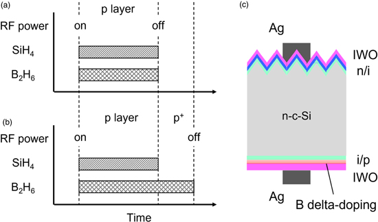
Fig. 1. Schematic deposition processes of the p-a-Si:H layers (a) without and (b) with B2H6 plasma treatment. (c) Schematic structure of the SHJ solar cell with the B2H6 plasma treatment.
Download figure:
Standard image High-resolution imageBoron concentrations (CB) and Si secondary ion intensity (ISi) were examined by a secondary ion mass spectroscopy (SIMS) system (ATOMIKA 4500) using O2 + ions of 0.5 keV as primary ion species. A boron ion implanted c-Si reference was used to evaluate CB in the heterostructures. Quasi-steady-state photoconductance measurements were performed in 1/64 generalized and transient modes (Sinton Instruments, WCT-120TS) to characterize the effective lifetime (τeff). 23,24)
2.2. Contact resistivity measurements
Single-side mirror-polished, Czochralski (Cz) grown, 400 μm thick p-type c-Si(100) substrates with a resistivity of 1–5 Ω·cm were cleaned by the same procedure as mentioned above. After the OPT, the i-a-Si:H and p-a-Si:H layers were deposited on the substrates. Then, the B2H6 plasma treatment was performed. Tungsten-doped indium oxide (IWO) was deposited at 100 °C with a metal mask by a reactive plasma deposition (RPD) system (Sumitomo Heavy Industries, Ltd., RPD-PCS4). A silver electrode was deposited using the same metal mask by sputtering. The PDA was carried out in the air using a hot plate at 200 °C for 30 min. Specific contact resistance (ρc) was derived from current–voltage (I–V) measurements with the transfer length method (TLM). 10–12,25)
2.3. Solar cell fabrication and characterization
Rear emitter SHJ solar cells were fabricated using as-sliced Cz-grown Si(100) wafers. After cleaning substrates by the standard cleaning method developed by RCA corporation (often referred to as the RCA cleaning process), 26) the etching process was carried out by 20 w/v% KOH solution at 70 °C for 10 min. Impurity guttering technique was done by a diffusion process using POCl3 at 900 °C for 15 min and a subsequent etching process using a mixture of HF and HNO3 acids. Then silicon oxide layers were deposited on the rear side of the substrates by atmospheric pressure CVD. Texturization was performed by a KOH-based solution at 80 °C for 20 min, and then pyramid textures were slightly rounded by HF/HNO3 mixed acid for 20 s. The silicon oxide layers on the rear side were stripped off by HF solution. Prior to the deposition of a-Si:H layers, the substrates were cleaned by the RCA cleaning process and dipped in 2.5% HF. Subsequently, the OPT mentioned above was conducted. The i-a-Si:H and n-a-Si:H were deposited on the front side, and then the i-a-Si:H and p-a-Si:H were deposited on the rear side by the PECVD system. After depositing the p-a-Si:H layer, the B2H6 plasma treatment was carried out as described above. IWO was deposited on both surfaces at 100 °C by the RPD system. Silver electrodes were prepared by screen-printing thermosetting silver paste, and post-annealing was performed in an oven at 200 °C for 30 min. The schematic of the complete SHJ solar cells is depicted in Fig. 1(c).
Current density–voltage (J–V) characteristics were measured using an I–V tester (Kyoshin Electric, KST-15Ce) under the 1 Sun illumination generated by a solar simulator (EKO Instruments Co., Ltd., SS-156XIL). External quantum efficiency (EQE) spectra were acquired by a spectral response measurements system (BUNKOH-KEIKI Co., Ltd., CEP-25MLR4).
2.4. Numerical simulation of solar cells
Numerical simulations of the band lineup were carried out by the AFORS-HET v2.5 simulation program. 27) The band lineups were calculated against the model shown in Fig. 1(c). The material parameters used in the numerical simulation are summarized in Table II. A thermionic emission model was employed at the a-Si:H/c-Si heterointerfaces, whereas the metal-semiconductor Schottky contact model was used at TCO/a-Si:H heterointerfaces. In the calculation, defects at the interfaces are not considered to simplify the calculations. The optical bandgap of a-Si:H is generally dependent on doping level, 28) the bandgap energy of the heavily B-doped layer was set to the same value as the p-a-Si:H layer since it was not experimentally determined. The band-to-band recombination coefficient was assumed to be zero in the calculation. This assumption is reasonable since carrier recombination in high-quality Si wafers is dominated by Auger recombination. 29) In addition, the neglect of band-to-band and Auger recombination process in a-Si:H layers is rationality. The a-Si:H contains the defect energy levels originating from dangling bonds within its bandgap, which induces the capture and recombination of many photogenerated carriers via the Shockley–Read–Hall recombination process. 30) Furthermore, assuming an ideal junction, the metal work function was set to the same values as the work function of the doped a-Si:H for simplification, meaning the effect of the work function of TCO is neglected.
Table II. Main parameters of the SHJ solar cells with and without the heavily B-doped layer used in numerical simulation.
| Parameters | n-c-Si | n-a-Si:H | p-a-Si:H | Heavily B-doped layer |
|---|---|---|---|---|
| Thickness (μm) | 180 | 0.005 | 0.005 a) | 0.001 |
| Electron affinity (eV) | 4.05 | 3.90 | 3.90 | 3.90 |
| Band gap (eV) | 1.12 | 1.72 | 1.72 | 1.72 |
| Doping density (cm−3) | 1.5 × 10¹⁶ | 7.1 × 10¹⁹ | 7.6 × 10¹⁹ | 8.4 × 10¹⁹ |
| Electron thermal velocity (cm s−1) | 1.0 × 10⁷ | 1.0 × 10⁷ | 1.0 × 10⁷ | 1.0 × 10⁷ |
| Hole thermal velocity (cm s−1) | 1.0 × 10⁷ | 1.0 × 10⁷ | 1.0 × 10⁷ | 1.0 × 10⁷ |
| Electron mobility (cm2 V−1 s−1) | 1111 | 20 | 20 | 20 |
| Hole mobility (cm2 V−1 s−1) | 421.6 | 5 | 5 | 5 |
| Band-to-band recombination coefficient (cm3 s−1) | 0 | 0 | 0 | 0 |
| Auger electron recombination coefficient (cm6 s−1) | 2.2 × 10⁻³¹ | 0 | 0 | 0 |
| Auger hole recombination coefficient (cm6 s−1) | 9.9 × 10⁻³² | 0 | 0 | 0 |
a) The layer thickness of p-a-Si:H in the solar cells without a heavily B-doped layer was set to 6.0 nm.
3. Results and discussion
Figure 2 shows the depth profiles of B concentration (CB) and Si secondary ions intensity (ISi) in the i-a-Si:H/p-a-Si:H/n-c-Si heterostructures fabricated (a) without and (b) with B2H6 plasma treatment. For the SIMS measurements, 30 nm thick, undoped a-Si:H layers were deposited on the p-a-Si:H surfaces to mitigate the modulation of the concentration at the surface. A unimodal CB peak was observed for the conventional heterostructure, whereas a bimodal CB peak was observed for the heterostructure employing the B2H6 plasma treatment. The CB peaks of ∼9 × 1020 cm−3 at about 36 nm are observed for the two structures, indicating that the peaks arise from the p-a-Si:H layer. The high CB peak of approximately 1 × 1021 cm−3 at 30 nm stemmed from the B2H6 plasma treatment. Interestingly, a bimodal CB peak was observed by using the B2H6 plasma treatment. We speculate that this dip in the CB peak was originated from reduction of input plasma power. A swift stop of SiH4 flow possibly causes a reduction in pressure, which leads to an unstable plasma state. The B was incorporated in an undoped a-Si:H protective layer at the order of 1018 cm−3 possibly due to residual B2H6 in the deposition chamber. This doping level is significantly lower than those of the p-a-Si:H layer, and thus the doping profiles were hardly affected by B in the protective layers. Therefore, a heavily doped p-a-Si:H layer was formed on the p-a-Si:H surface by the B2H6 plasma treatment.
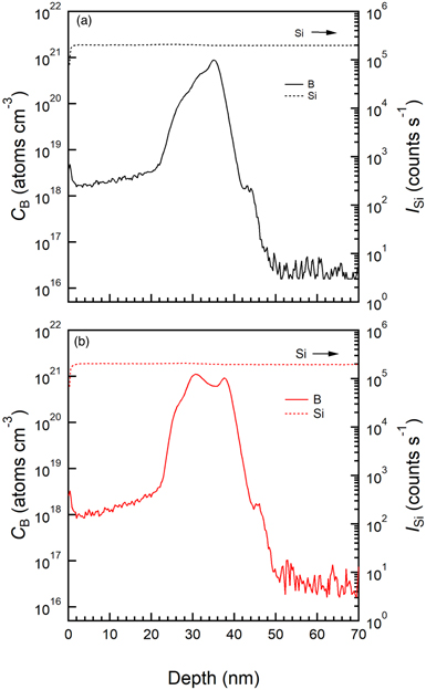
Fig. 2. SIMS depth profiles of B concentration and Si secondary ion intensity for the i-a-Si:H/p-a-Si:H/n-c-Si heterostructures (a) without and (b) with B2H6 plasma treatment. The dotted lines represent the Si secondary ion intensity.
Download figure:
Standard image High-resolution imageFigure 3 shows the I–V characteristics of the Ag/IWO/p-a-Si:H/i-a-Si:H/p-c-Si heterostructures (a) without and (b) with the B2H6 plasma treatment after post-annealing at 200 °C for 30 min. The inset shows the schematic sample structure for TLM measurements. Figure 3(c) shows the total resistance (Rtotal) derived from the I–V characteristics as a function of electrode spacing (d). In the conventional TLM model, Rtotal and ρc are expressed as follows,


where Rsh is the sheet resistance of the Si substrate, W is the electrode width, Rc is the contact resistance, and LT is the transfer length. The ρc values of the samples without and with the B2H6 plasma treatment were 2.793 and 0.859 Ω‧cm2, respectively. The ρc was reduced to about one-third by the heavily B-doped layer.
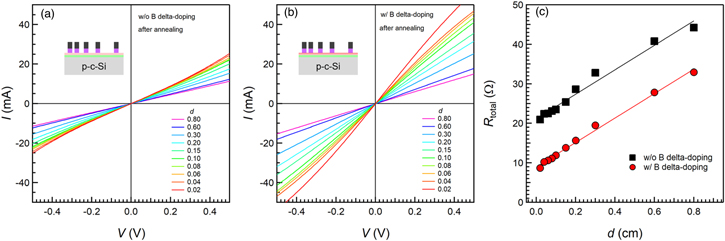
Fig. 3. Current–voltage characteristics of the Ag/IWO/p-a-Si:H/i-a-Si:H/p-c-Si heterostructures (a) without and (b) with a heavily B-doped layer after post-annealing at 200 °C for 30 min. The insets show the schematic sample structure for TLM measurements. (c) The total resistance derived from the I–V characteristics as a function of electrode spacing.
Download figure:
Standard image High-resolution imageHall measurements were carried out for the IWO layer before and after post-annealing at 200 °C for 30 min. The electron density, mobility, and resistivity of the IWO layer are summarized in Table III. The electron density and mobility are slightly improved after the post-annealing, which is ascribed to the crystallization of the IWO layer and an increase in activated dopants. Figure 4 shows (a) the schematic structures of the Ag/IWO heterostructure for TLM measurements. I–V characteristics of the heterostructures (b) before and (c) after annealing at 200 °C for 30 min (d). Total resistance (Rtotal) of the heterostructures as a function of electrode distance (d) before and after annealing at 200 °C for 30 min. From Fig. 4(d), the slopes of the linear regression became smaller after annealing, meaning the Rsh of the IWO layer became smaller. This reduced Rsh is explained by the reduced resistivity observed by Hall measurements without contradiction. Note that the decreasing rate of Rsh values measured by TLM before and after annealing was smaller than that obtained from Hall measurements. This difference is possibly arisen from currents from the side of the pads in addition to current between pad electrodes, which contribute to reduce the resistance. The decrease in resistivity due to annealing enhances currents from the side of the pads. Furthermore, the resistance may have fluctuated due to a deviation of the electrode size from the design value for the Hall and TLM measurements. These effects result in the large decreasing rate of Rsh in the TLM measurement than the Hall measurement. The ρc values were slightly improved from 0.024 to 0.016 Ω‧cm2 after the post-annealing. The ρc value of the Ag/IWO structure was significantly smaller than that of the IWO/p-a-Si:H/i-a-Si:H heterostructure, indicating that the contact resistance of the heterostructures was dominated by the IWO/p-a-Si:H/i-a-Si:H heterointerfaces.
Table III. Electron density, mobility, and resistivity of the IWO layer before and after annealing at 200 °C for 30 min.
| Electron density (cm−3) | Mobility (cm2 V−1 s−1) | Resistivity (Ω cm) | |
|---|---|---|---|
| Before annealing | 2.47 × 10²⁰ | 49.2 | 5.14 × 10⁻⁴ |
| After annealing | 2.57 × 10²⁰ | 58.3 | 4.17 × 10⁻⁴ |

Fig. 4. (a) Schematic structures of the Ag/IWO heterostructure for TLM measurements. Current–voltage characteristics of the heterostructures (b) before and (c) after annealing at 200 °C for 30 min. (d). Total resistance (Rtotal) of the heterostructures as a function of electrode distance (d) before and after annealing at 200 °C for 30 min.
Download figure:
Standard image High-resolution imageFigure 5 shows (a) J–V curves and (b) EQE of the SHJ solar cells with and without the B2H6 plasma treatment. As can be readily seen, the J–V characteristics are improved by using the B2H6 plasma treatment. The short-circuit current density (JSC), VOC, fill factor (FF), conversion efficiency (η), series resistance (Rs), shunt resistance (Rp), and ideal factor (n) are summarized in Table IV. The Rs, Rp, and n were determined by comparing the I–V curve of a solar cell at one Sun with the one at 0.1 Sun. 31) The B2H6 plasma treatment significantly improved FF due to lower Rs and higher Rp. Furthermore, there were no remarkable differences in EQE spectra between the SHJ solar cells with and without B2H6 plasma treatment. Figure 6 shows τeff of symmetrically passivated c-Si using the B2H6 plasma treatment as a function of minority carrier density (MCD). The τeff at MCD of 1 × 1015 cm−3 was improved from 1.4 to 2.1 ms by employing the B2H6 plasma treatment. The implied VOC (i-VOC) was 0.694 V and 0.695 V for the sample without and with the B2H6 plasma treatment, respectively. Almost identical i-VOC was obtained irrespective of the B2H6 plasma treatment, suggesting that the difference in the passivation performances between both is less distinct at high injection level. On the other hand, the passivation performance at low injection level was enhanced by using the B2H6 plasma treatment. The improvement in solar cell performance shown in Fig. 5(a), i.e. improved FF, can be explained by the improved passivation performance at low injection level. Hence, the B2H6 plasma treatment can reduce resistive loss without sacrificing passivation performance. The reduced resistive loss is attributed to the lowered resistance of the p-a-Si:H layer and contact resistance at the IWO/p-a-Si:H heterointerfaces, as shown in Fig. 3. In addition, the reduction of leak current and recombination at the heterointerfaces seem to be responsible for the improved FF, since decreased n was observed for the sample with the heavily B-doped layer.
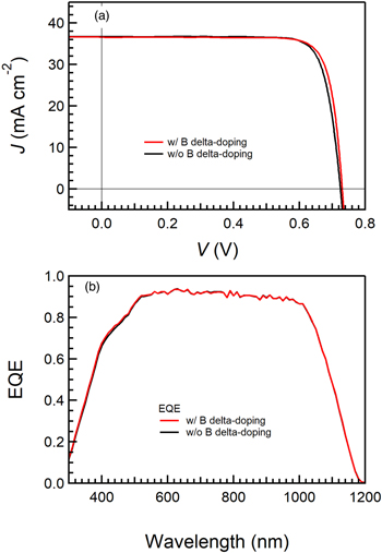
Fig. 5. (a) Current density–voltage curves of the SHJ solar cells and (b) EQE of the SHJ solar cells with and without a heavily B-doped layer.
Download figure:
Standard image High-resolution imageTable IV. Short-circuit current density JSC, open circuit voltage VOC, fill factor FF, conversion efficiency η, series resistance Rs, series resistance Rp, and ideal factor n of the SHJ solar cells with and without the heavily B-doped layer.
| Heavily B-doped layer | JSC (mA cm−2) | VOC (V) | FF | η (%) | Rs (mΩ) | Rp (Ω) | n |
|---|---|---|---|---|---|---|---|
| With | 36.6 a) | 0.726 | 0.816 | 21.7 | 2.2 | 1194 | 1.05 |
| Without | 36.5 a) | 0.725 | 0.804 | 21.2 | 2.7 | 832 | 1.11 |
The parameters are averaged values of four fabricated solar cells.
a) The cell area is 15.6 × 15.6 cm2.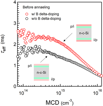
Fig. 6. Injection-dependent effective carrier lifetime of the heterostructures with and without B2H6 plasma treatment before annealing at 200 °C for 30 min. The insets represent the schematic structures of both two samples.
Download figure:
Standard image High-resolution imageFigure 7 shows the numerically simulated band diagrams of the n-c-Si/p-a-Si:H/IWO heterointerfaces (a) without and (b) with the B2H6 plasma treatment by the AFORS-HET simulator. Their band diagrams were obtained at each maximum power point (MPP) under 1-Sun illumination. It is seen that upward band bending is enhanced by employing the B2H6 plasma treatment in Fig. 7(b) compared with Fig. 7(a). This is probably caused by the increase in Fermi energy difference between p-a-Si:H and n-c-Si and the suppression of the depleted region in p-a-Si:H at the TCO/p-a-Si:H heterointerface owing to the higher hole concentration in the heavily B-doped layer. The upward band bending is responsible for the mitigated resistive loss and subsequently increased FF observed in Fig. 5. Note that the band diagrams are idealized. The impact of the TCO work function was not considered since ideal TCO/p-a-Si:H contact was assumed. Furthermore, the doping levels of the heavily B-doped layer and the p-layer are not accurate. Since the activated doping level was unclear, the doping levels were referred to as the peak B concentration shown in Fig. 2 and they were modified to simulate conversion efficiency in Table IV. The work function of TCO and the concentration of activated dopants affect the real band diagrams. The simulated J–V curves of both two solar cells are shown in Fig. 8 and the solar cell parameters are summarized in Table V. The VOC and FF, and consequently η were improved by employing the B2H6 plasma treatment. The improved VOC in the numerical simulation was probably attributed to the assumption of no defects at the heterointerfaces.
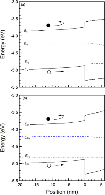
Fig. 7. Numerically simulated energy-band diagrams of the SHJ solar cells (a) without and (b) with a heavily B-doped layer at each MPP. EC, EV, EFn, and EFp represent conduction band energy, VB energy, quasi-Fermi energy of electrons, and holes, respectively. The position of the n-c-Si/p-a-Si:H heterointerfaces was set to zero.
Download figure:
Standard image High-resolution image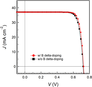
Fig. 8. Simulated J–V curves of the heterojunction solar cells with and without a heavily B-doped layer by the AFORS-HET v2.5 simulation program.
Download figure:
Standard image High-resolution image
Table V. Calculated JSC, VOC, FF, η of the SHJ solar cells with and without the heavily B-doped layer by the AFORS-HET v2.5 simulation program.
| Heavily B-doped layer | JSC (mA cm−2) | VOC (V) | FF | η (%) |
|---|---|---|---|---|
| With | 37.1 | 0.728 | 0.821 | 22.15 |
| Without | 37.1 | 0.721 | 0.806 | 21.52 |
The efficient hole collection is caused by facilitated tunneling from c-Si to p-a-Si:H and the recombination junction of the TCO/p-a-Si:H interface. It is considered that the extraction of holes in c-Si is ruled by tunneling from c-Si to p-a-Si:H via i-a-Si:H, work function matching between TCO and p-a-Si:H, and trap-assisted tunneling (TAT) at the TCO/p-a-Si:H. 12,32) Since the VB offset of 400–600 meV is created at the a-Si:H/c-Si heterointerface, 33,34) tunneling of holes through the i-a-Si:H layer is required. The upward band bending observed in Fig. 7(b) suppresses band flattening at the MPP, which facilitates the tunneling from c-Si to p-a-Si:H. Furthermore, electrons can be repelled out of the n-c-Si/p-a-Si:H heterointerface as a by-product of the enhanced upward band bending, and hence carrier recombination at the a-Si:H/c-Si interface is reduced. It is known as well that the work function mismatch between TCO and p-a-Si:H results in a depleted a-Si:H due to the comparatively low carrier density of p-a-Si:H than that of TCO. Heavily doped p-a-Si:H, as observed in Fig. 2(b) can render the depletion width in the p-a-Si:H layer narrow. Furthermore, recombination between holes in p-a-Si:H and electrons in TCO is necessary for solar cell operation via TAT, since the majority carrier of TCO and p-a-Si:H are electrons and holes, respectively. It is reported that energy states in doped a-Si:H are additionally introduced near the band edges by heavy doping, 35,36) suggesting many trap states are created on the p-a-Si:H surface by the B2H6 plasma treatment. Hence, the heavily B-doped layer would lead to efficient tunneling of holes across i-a-Si:H by enhancement of the upward band bending, resulting in hole accumulation at the TCO/p-a-Si:H heterointerface. The accumulated holes can readily recombine with electrons in TCO via the increased trap states in the heavily B-doped layer. These results reduce the ρc of the heterostructures with heavily doped p-a-Si:H, as observed in Fig. 3(c). Note that the ρc obtained by TLM measurements includes the contact resistance contributed by the tunneling from c-Si to p-a-Si:H and the exchange between holes in p-a-Si:H. Therefore, the reduced ρc would stem from enhanced tunneling processes at the IWO/p-a-Si:H/i-a-Si:H/c-Si heterointerfaces, leading to increased FF and thus improved conversion efficiency.
4. Conclusions
In conclusion, we investigated the impact of the B2H6 plasma treatment on the structural and electrical properties of p-a-Si:H/i-a-Si:H/c-Si heterostructures and the performance of the SHJ solar cells. The B2H6 plasma treatment is demonstrated by continuous B2H6 flows with RF power after depositing the p-a-Si:H layer. The SIMS measurements revealed an increase in B concentration at the p-a-Si:H surface by employing the B2H6 plasma treatment. Furthermore, specific contact resistance is decreased by about one-third owing to the B2H6 plasma treatment. These results indicate that B is heavily doped at the p-a-Si:H surface. No degradation of passivation performance is observed in the presence of the heavily B-doped layer. The η of SHJ solar cells with the heavily B-doped layer is improved by a higher FF than that without the heavily B-doped layer due to decreased Rs and increased Rp. Numerical simulations reveal that the upward band bending at the TCO/p-a-Si:H heterojunction is enhanced by the heavily B-doped layer. The enhanced upward band bending is responsible for the decrease in Rs and increases in Rp owing to facilitated tunneling holes from c-Si in the p/i-a-Si:H layers and the TCO/p-a-Si:H heterointerface. We propose the B2H6 plasma treatment, adaptable to the conventional fabrication procedures of SHJ solar cells. This process can improve TCO/p-a-Si:H contact properties without sacrificing its passivation performance and consequently produce high-performance SHJ solar cells.
Acknowledgments
This work was supported by the New Energy and Industrial Technology Development Organization (NEDO).