
Abstract
To avoid formation of the photo-inactive δ-phase of formamidinium-cesium lead triiodide, copper or germanium was added to the perovskite compounds to stabilize the photoactive α-phase. It was found that the substitution of lead by germanium (Ge) or copper (Cu) provided the stabilization of the α-phase in the present work. The first-principles molecular dynamics calculations indicated that displacements of formamidinium molecules were suppressed by the Ge doping. X-ray diffraction results indicated that the Ge or Cu doping of the perovskite compounds could be effective for suppression the phase transition from α- to δ-phase.
Export citation and abstract BibTeX RIS
1. Introduction
Organic-inorganic hybrid perovskite solar cells (PSCs) are being studied worldwide as next-generation solar cells due to their high conversion efficiencies and easy fabrication method. 1–4) PSCs consist of ABX3-type crystals, where A is the organic (or inorganic) cation such as methylammonium (MA), formamidinium (FA), ethylammonium (EA), guanidinium (GA), rubidium (Rb), or cesium (Cs), B is a metal cation such as Pb or Sn, and X is a halide anion such as I, Br, or Cl. 5–7) To develop commercial solar cells, the photovoltaic properties and long-term stabilities have been improved by material design or control of compositions. 7–11) Ionic liquids have been applied for the fabrication of efficient and stable perovskite photovoltaics. 12) Although CH3NH3PbI3 (MAPbI3) PSCs show excellent device properties, desorption of MA cations reduce the long-term stability of the devices. 13–15)
FACs perovskite crystals, which consist of FA and Cs as A-site cations, have provided high efficiencies and stabilities. 16,17) However, owing to the photo-inactive δ-phase of FACs perovskite crystals, optimization of compositions and formation conditions of thin films is the big issue. 18–20) Substitution of Pb by other elements such as Sn, 21–23) Cu, 24–27) Co, 28,29) Ni, 30) Mn, 30,31) Zn, 32,33) Ge, 34,35) Eu, 36,37) or Sb 38,39) would be one of the method to optimize the electronic and crystal structures and to improve the photovoltaic properties. For example, the addition of a small amount of Sn to FACs perovskite crystals suppresses the phase transition from α- to δ-phase, which resulted in extended carrier lifetime and less temperature dependence. 40) Recently, first-principles calculations have also been used to estimate the electronic structures and photovoltaic properties, which have been verified experimentally. 41–44)
The aim of this work is to fabricate and characterize FACs perovskite photovoltaic devices with added Ge or Cu. Effects of Ge or Cu addition to the FACs crystal were investigated by X-ray diffraction, scanning electron microscopy (SEM)/scanning electron energy dispersive spectroscopy (EDS), photovoltaic measurements, and first-principles calculation. The electronic structures, band structures, and partial density of states (pDOS) of Ge or Cu-introduced perovskite crystals were examined on stabilities, effective mass, and charge transfer by Born–Oppenheimer molecular dynamics calculations (BOMD) and band calculation. Molecular motion behavior and thermodynamic stabilities of Ge, Cu, and organic cations were also investigated by Car-Parrinello molecular dynamics calculations (CPMD). The electronic structures and thermodynamic stabilities were compared by these first-principles calculations and experimental results.
2. Experimental and calculation methods
The present PSCs were prepared by the same method as reported in the previous works. 45–47) For preparing the perovskite compound, a mixture of CH5N2I (FAI, Sigma Aldrich), CsI (Daiichi Kigenso Kagaku Kogyo), PbI2 (Sigma Aldrich), PbCl2 (16.7 mg, Sigma Aldrich), CuBr2 (Sigma Aldrich), GeI2 (Sigma Aldrich), N-methyl-2-pyrrolidinone (NMP, 100 μl, Fujifilm Wako Pure Chemical) with the desired molar ratio in N,N-dimethylformamide (DMF, Nacalai Tesque, 0.5 ml) was stirred at 70 °C for 24 h. As a standard device, the compositions of FAI, CsI and PbI2 in DMF were adjusted to be 0.966 M (85.6 mg), 0.204 M (26.5 mg) and 1.2 M (276.6 mg). For the 2% CuBr2 added device, the compositions of FAI, CsI, PbI2 and CuBr2 were adjusted to be 0.996 M (85.6 mg), 0.204 M (26.5 mg), 1.176 M (271.1 mg) and 0.024 M (2.7 mg). For the 2% GeI2 added device, the mole of FAI, CsI, PbI2 and GeI2 was adjusted to be 0.996 M (85.6 mg), 0.204 M (26.5 mg), 1.176 M (271.1 mg) and 0.024 M (3.9 mg). The perovskite solutions were spin-coated on TiO2 with air-blow at three times. 46,47) A solution of decaphenylcyclopentasilane (DPPS, Osaka Gas Chemical, OGSOL SI-30–15, 20 mg) was prepared in chlorobenzene (1.0 ml) and dropped onto the perovskite layer during the last stage of the spin-coating process. 48–50) DPPS was used as a hole-transporting material to protect the cell from moisture and oxygen. 48) Then, the substrate was annealed at 150 °C for 10 min. All procedures were performed in air atmosphere. A gold (Au) electrode was deposited as the top electrode. The structure of the solar cells is denoted as FTO/TiO2/perovskite/DPPS/spiro-OMeTAD/Au. The prepared cells were stored at a temperature of 22 °C and humidity below 30%.
The perovskite crystals with supercells of 2 × 2 × 2 as cluster models were constructed, as reported in the previous works. 51–54) The molecular behavior and thermodynamic stabilities of Ge, Cu and organic cations were calculated by CPMD. After equilibration of the electronic and atomic states, MD calculations were performed at a constant temperature of 300 K. Planewave basis set cut offs for the wave functions and charge density were set at 50 and 200 Rydberg. Pseudopotential function is PBE of NCPP type. Molecular motions were traced to 0.1088 ps. The electronic structures, band structures, and pDOS of Cu- or Ge-incorporated perovskite crystals were examined by BOMD and band calculation. The uniform k-point grid (4 × 4 × 4) in the Brillouin zone was used to calculate the electronic structures and pDOS. For the Cu- or Ge-incorporated perovskite crystals with 2 × 2 × 2 supercells, one of the Pb atoms was substituted with a Cu or Ge at the center of the supercell.
3. Results and discussion
3.1. First-principles calculations
A structure model of cubic FA0.875Cs0.125PbI3 perovskite (α-phase) with 2 × 2 × 2 supercell is shown in Fig. 1(a). Perovskite cubic crystals with partial substitution of Cu or Ge at the Pb site are shown in Figs. 1(b) and 1(c), respectively. Cu or Ge-doped perovskite crystals were analyzed by the first-principles CPMD calculations.
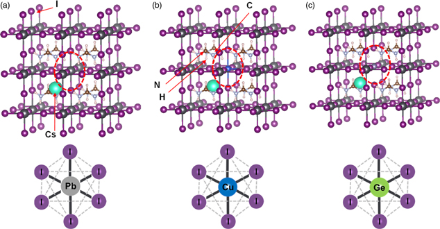
Fig. 1. Crystal structures of (a) FA0.875Cs0.125PbI3 (b) FA0.875Cs0.125Pb0.875Cu0.125I3, and (c) FA0.875Cs0.125Pb0.875Ge0.125I3.
Download figure:
Standard image High-resolution imageAfter equilibrating electronic and nucleus state at 0 K, total energies and the relaxation process of kinetic energies were calculated at 300 K. The states of equilibrium are shown in Fig. 2. The relaxation process of the total energies of α- and δ-phases is shown in Fig. 2(a). The total energies indicate needed energy to form the stable crystal. The relaxation process of total energies at 300 K shows that the system reached equilibrium at 0.036 ps. The lowest total energies of the Ge-doped or Cu-doped cubic crystals were −3423.5 and −3559.7 eV cell−1, respectively. The partial substitution increased the total energies compared with crystals without additives, and reduced the stabilities of the cubic perovskite structures. To estimate the structural stability of the perovskite compounds, an indicator called the tolerance factor (t) has been calculated and used. 7) Based on the many previous studies on the perovskite compounds, the perovskite structure could be experientially formed in the range of 0.813 < t < 1.1. The t-factors and total energies of the perovskite crystals in the present work are summarized in Table I. The calculated total energies of the phase transition from α-phase to δ-phase at 300 K are all negative values in all systems. This indicates that the δ-phase is more stable than the α-phase. Therefore, it is necessary to provide an energy barrier between the α-phase and δ-phase to prevent the phase transition to the δ-phase.
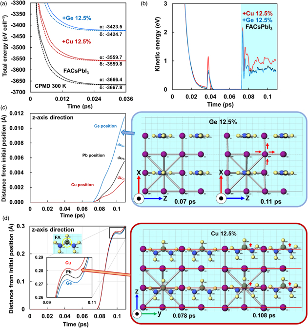
Fig. 2. Molecular dynamics calculations of perovskite crystals. (a) Total energies, (b) kinetic energies, and (c) displacements of Pb, Cu and Ge positions along z-axis. (d) Displacements of the C position in FA along z-axis.
Download figure:
Standard image High-resolution imageTable I. Calculated t-factors and total energies (Etot) of α-phase and δ-phase perovskites.
| t-factor | Etot α (eV) | Etot δ (eV) | Etot (δ-α) (eV) | |
|---|---|---|---|---|
| FA0.875Cs0.125PbI3 | 0.970 | −3666.4 | −3667.8 | −1.4 |
| FA0.875Cs0.125Pb0.875Ge0.125I3 | 0.986 | −3423.5 | −3424.7 | −1.2 |
| FA0.875Cs0.125Pb0.875Cu0.125I3 | 0.986 | −3559.7 | −3559.8 | −0.1 |
The kinetic energies of the atoms in the Ge-doped crystal are shown in Fig. 2(b). Large fluctuations in kinetic energy are observed in the 0.07 ps of the relaxation process. The behavior of the kinetic energies was suppressed in the Ge-doped crystals and enhanced in the Cu-doped crystals, as shown in Figs. 2(c) and 2(d), respectively. Differences in the kinetic energies affect carrier diffusion and charge transfer due to change in the strength of the bonds between the central metal and ligand. Distances from the initial positions of carbon (C) in FA, Pb, Cu and Ge are shown in Fig. 2(c). The Cu-doped crystals showed smaller deviations of the Cu atoms from their initial positions and smaller distortions for the CuI6 octahedron. As a result, a significant change is observed at the position of C in FA. On the other hand, a large shift from the initial Ge position is observed for the Ge-doped crystal, resulting in the significant strain in the crystal. Then, the deviation of C positions in FA was suppressed. Differences in the strength of the bonds between the central metal and I and the orientation of the orbitals caused differences in the distortion, which would change the interaction between the FA molecule and I, changing the kinetic behavior of the FA. These differences in orbital interactions should affect the phase transition and charge transfer.
BOMD calculations for Cu- or Ge-doped crystals were performed to calculate the band structures, pDOS and electron density distribution for each system after structural optimization at 300 K. These results are shown in Fig. 3. The band gaps and effective mass of the hole are listed in Table II. As observed in Fig. 3(a), 5p orbitals of I atom and 6p orbitals of the Pb atom dominate near the valence band maximum (VBM) and conduction band minimum (CBM), respectively. For the Cu-doped perovskite in Fig. 3(b), the 5p orbitals of I atom and 3d orbitals of the Cu atom dominate near the VBM. The 6p orbitals of the Pb atom and the 3d orbitals of the Cu atom dominate near the CBM. The bandgap energy (Eg) of the Cu-doped crystal of 0.78 eV is lower than 0.99 eV for the non-doped perovskite. The effective mass ratio of hole (mh*) of 0.011 for the Cu-doped crystal is slightly higher than that of the non-doped crystal due to the localization of the 3d orbitals of Cu near the VBM and CBM. The localization of the 3d orbital of Cu near the VBM and CBM suppressed the carrier generation and diffusion, which would reduce short-circuit current density (JSC). For the Ge-doped crystals in Fig. 3(c), the 6p orbital of the Pb atom and the 4p orbital of the Ge atom overlap and dominate in the conduction band. The Eg and mh* were 0.92 eV and 0.0098, respectively, which was almost the same as the non-doped crystal. The electron density distribution of the 5p orbital of the I atom and the 4p orbital of the Ge atom are shown in Fig. 3(c). Charge transfer from 5p orbital of the I atom to 4p orbital of the Ge atom would promote carrier generation and transfer and improve the JSC. These results indicate that Ge-doped FACsPbI3 PSCs would have better photovoltaic properties.
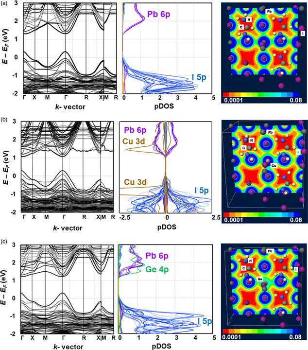
Fig. 3. Calculated band structures, partial density of state, and electron density distribution of (a) FA0.875Cs0.125PbI3, (b) FA0.875Cs0.125Pb0.875Cu0.125I3, and (c) FA0.875Cs0.125Pb0.875Ge0.125I3.
Download figure:
Standard image High-resolution imageTable II. Calculated band gaps and effective mass of hole for the present perovskite crystals.
| Crystal | Eg (eV) | mh*/m0 |
|---|---|---|
| FA0.875Cs0.125PbI3 | 0.994 | 0.0095 |
| FA0.875Cs0.125Pb0.875Ge0.125I3 | 0.920 | 0.0098 |
| FA0.875Cs0.125Pb0.875Cu0.125I3 | 0.781 | 0.0110 |
3.2. Device characterization
FACsPbI3 based PSCs added with 2% Cu, 2% Ge, 12.5% Cu, or 12.5% Ge were fabricated and characterized. A cross-sectional schematic illustration of the present PSC is shown in Fig. 4(a). The XRD patterns of these cells are shown in Fig. 4(a). For the device doped with 2% Cu, weak diffraction peaks of the photoactive α-phase were observed, and the photo-inactive δ-phase was formed as observed at 2θ of 12.6°. On the other hand, sharp 100 diffraction peaks of the α-phase are observed for the cells doped with 2% Ge, 12.5% Ge, and 12.5% Cu, which indicates formation of the δ-phase was suppressed, and the structure of α-phase was maintained. Since additions of a small amount of Ge and Cu had little effect on the strain of the crystal lattice, the addition of 2% increased the precipitation of the δ-phase by the reduction of the effect of crystal strain.

Fig. 4. (a) Cross-sectional schematic of the present perovskite solar cell. (b) XRD patterns of present perovskite crystals. (c) J–V characteristics of perovskite photovoltaic devices. (d) Changes of conversion efficiencies of the present cells.
Download figure:
Standard image High-resolution imageJ–V characteristics of the devices are shown in Fig. 4(b), and the photovoltaic parameters are listed in Table III. The device doped with Cu provided the lowest photovoltaic performance, and the formation of the photo-inactive δ-phase caused reduction in the photovoltaic properties. Especially, the significant reduction in JSC would be due to the suppression of carrier diffusion by the localization of the 3d orbitals of the Cu atom. For the device doped with 2% Ge, JSC, VOC and FF were higher than those of the Cu-doped devices. The effective mass of the hole increased in the Ge-doped crystal compared to that of the non-additive crystal, as listed in Table I, and the JSC was decreased by the lower carrier diffusion. Although the photovoltaic properties of Cu-doped devices were inferior to non-doped device, α-phase was formed for the device doped with 12.5% Cu. When Ge was added up to 12.5%, the α-phase was formed without δ-phase, indicating Ge can be a candidate as an alternative element to Pb. The stability of the conversion efficiencies is shown in Fig. 4(c). Similar changes are observed for these devices.
Table III. Photovoltaic parameters of the present photovoltaic devices.
| Devices | Notation | JSC (mA cm−2) | VOC (V) | FF | η (%) | ηave (%) | Lattice constant (Å) |
|---|---|---|---|---|---|---|---|
| FA0.83Cs0.17PbI3 | — | 19.3 | 0.815 | 0.496 | 7.74 | 7.66 | 6.299(2) |
| FA0.83Cs0.17Pb0.98Ge0.02I3 | Ge 2% | 16.7 | 0.770 | 0.504 | 6.42 | 6.32 | 6.310(0) |
| FA0.83Cs0.17Pb0.875Ge0.125I3 | Ge 12.5% | 13.1 | 0.747 | 0.422 | 4.13 | 3.77 | 6.325(1) |
| FA0.83Cs0.17Pb0.98Cu0.02I3 | Cu 2% | 12.2 | 0.702 | 0.350 | 3.00 | 2.46 | 6.345(3) |
| FA0.83Cs0.17Pb0.875Cu0.125I3 | Cu 12.5% | 0.583 | 0.0385 | 0.237 | 0.00532 | 0.0039 | 6.255(5) |
SEM images and corresponding EDS elemental mappings of the present solar cell devices are shown in Fig. 5. SEM images show differences in crystallinity for each composition. In particular, the grain sizes increased by the Ge and Cu addition, as shown in Figs. 5(c) and 5(e). The grain size of the FA0.83Cs0.17Pb0.875Ge0.125I3 perovskites is the largest, which indicates the smallest grain boundaries. Elemental mapping images show that both Ge and Cu were distributed uniformly in the perovskite grains.
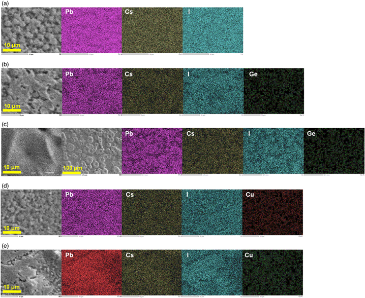
Fig. 5. SEM images and corresponding elemental mappings of the Cs K, Pb M, Ge K, Cu K, and I L lines of (a) FA0.83Cs0.17PbI3, (b) FA0.83Cs0.17Pb0.98Ge0.02I3, (c) FA0.83Cs0.17Pb0.875Ge0.125I3, (d) FA0.83Cs0.17Pb0.98Cu0.02I3 and (e) FA0.83Cs0.17Pb0.875Cu0.125I3 devices.
Download figure:
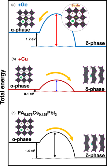
Standard image High-resolution imageSchematic models of the phase transitions from α- to δ-phase of the FA0.875Cs0.125Pb0.875Ge0.125I3 and FA0.875Cs0.125Pb0.875Cu0.125I3 crystals are shown in Fig. 6. The calculated total energies of the phase transition from the α- to δ-phase show that the δ-phase is more stable than the α-phase. However, the strain effect by the Ge addition observed in the molecular dynamics calculations in Fig. 2(c) provided crystal distortion for the GeI6 octahedron, which resulted in reducing the FA displacement. This causes the interaction between I and FA, creating an energy barrier between the α- and δ-phase, which leads to the suppression of the α- to δ-phase transition as shown in Fig. 6(a). On the other hand, when Cu was added to the FA0.875Cs0.125PbI3, less distortion for the CuI6 octahedron and less molecular displacement of FA were observed, as shown in Fig. 2(d). The increased kinetic energy of the FA molecules facilitated the phase transition from α- to δ-phase, as illustrated in Fig. 6(b). The energy barrier between the α- and δ-phases reduced due to the strain relaxation compared to the standard FA0.825Cs0.125PbI3, which leads to the α-δ phase transition. It is also considered that the present 2 × 2 × 2 superstructure would be a kind of the meta-stable phase. When a small amount (∼2 at%) of Ge or Cu were added to the FA0.875Cs0.125PbI3 crystal, degrees of the crystal symmetry were reduced, which would lead to a reduction of the energy barrier between the α- and δ-phases.
Fig. 6. Schematic illustrations of phase transitions of (a) FA0.875Cs0.125Pb0.875Ge0.125I3, (b) FA0.875Cs0.125Pb0.875Cu0.125I3, and (c) FA0.83Cs0.17PbI3.
Download figure:
Standard image High-resolution image
4. Conclusions
It was found that substitutions of Pb by Cu or Ge affected the stabilization of the α-phase. The strain for the PbI6 octahedra was relaxed by the Cu doping, which increased the displacement of FA molecules, resulting in increasing the kinetic energy. The 3d orbitals of Cu were localized near the CBM and VBM, which suppressed carrier diffusion resulting in lower JSC and η. The structural distortion for PbI6 octahedra was caused by the Ge doping, which decreased the displacement of FA molecules, resulting in a decrease in the kinetic energy. Suppression of formation of δ-phase resulted in formation of α-phase. Electron density distribution showed the charge transfer from Ge to I ions, which promoted carrier diffusion from I 5p to Ge 4p orbitals. The PSCs doped with 12.5% Ge also provided photovoltaic properties.
Acknowledgments
The authors would like to acknowledge Dr. T. K., Daiichi Kigenso Kagaku Kogyo Co., Ltd., for providing CsI. This research was supported by JSPS KAKENHI Grant No. JP 21K05261.