
Abstract
We report on the effective passivation of cut edges of n-type (100) crystalline silicon by forming thin oxide layers achieved by heat treatment in liquid water at 90 °C for 2 h followed by heating in an air atmosphere at 300 °C for 1 h. The mechanical cut with the (110) oriented cleaved edge markedly decreased the photo-induced effective minority carrier lifetime τeff to 6.9 × 10⁻⁴ s, which was 0.22 times the initial value of 3.2 × 10⁻³ s, and which was maintained by the region 0.5 cm away from the edge. The present passivation treatment resulted in the reduction of τeff to 0.43, with τeff values of 4.0 × 10⁻⁴ s at the edge and 9.4 × 10⁻⁴ s at 0.2 cm from the edge. The analysis with a simple model of carrier diffusion in the lateral direction resulted in the recombination velocity at the cut edge, which was initially higher than 2000 cm s−1, being decreased to 50 cm s−1 by the present treatment, while the recombination velocity at the sample surface was increased from 8 (initial) to 46 cm s−1, probably due to the field-induced depletion effect.
Export citation and abstract BibTeX RIS
1. Introduction
The process of semiconductor surface passivation is important for manufacturing high-performance photo-sensors and photovoltaic devices. 1–9) A passivation layer can reduce the density of carrier recombination defect states and improve the lifetime of photo-induced minority carriers. Many passivation technologies, formation of thermally grown SiO2 layers, hydrogenation treatment, and field-effect passivation caused by induced charges at the interfaces of SiN/Si or Al2O3/Si, have been developed. 10–22) Thermally grown SiO2, formed by oxidizing the silicon surface above 1000 °C, makes an excellent surface passivation layer with a stable SiO2/Si interface and a low density of carrier recombination defect states. 11) Hydrogenation treatment terminates dangling bonds at silicon surfaces and decreases the surface recombination velocity. The hydrogenation treatment is an attractive passivation technique for low-temperature processing; however, it is unstable owing to the oxidation of Si–H bonds in general. Due to the fact that after device fabrication, semiconductor substrates are cut into small pieces for application to equipment, 23–25) the passivation of cut edge surfaces is also important at a low temperature to maintain an excellent device performance. We have previously reported that a mechanical cut surface had a high recombination velocity of above 500 cm s−1, which reduced the effective photo-induced minority carrier lifetime in a 0.9 cm wide region near the cut edge. 26) Following this study, our attempts at passivation of a cut edge of crystalline silicon by plasma hydrogenation as well as 1.3 Mpa H2O vapor heat treatment at 270 °C 27–29) were unfortunately not successful, probably because the passivated oxide layers were not well formed over the cut edge surface, possibly owing to the surface roughness. We recently developed a heat treatment method in liquid water at temperatures ranging from 90 °C to 110 °C for low-temperature surface passivation. 30–32) The formation of a 0.7 nm thick passivation oxide layer on the silicon surfaces was achieved, with an effective minority carrier lifetime τeff longer than 1 ms. The high τeff values were maintained for at least 2 months when the samples were kept in air atmosphere at RT. The thickness of the oxide layer formed by this treatment was thinner than that obtained using other low-temperature chemical oxidation processes, such as nitric acid oxidation of Si. 33) However, a thin passivation layer with a low recombination velocity is attractive, for example, in the application of metal-insulator-semiconductor-type solar cells because of the requirement to collect tunneling current from the semiconductor to the metal. In addition, as compared to the chemical oxidation processes handling the hazardous chemicals, the liquid water heat treatment has the advantages of being safer and easier to dispose of waste liquid. It is expected to lead to cost savings for industrial processing.
We reported on our first trial of passivation of mechanically cut edges of crystalline silicon by heat treatment in liquid water at the 33rd International Photovoltaic Science and Engineering Conference (PVSEC-33). 34) In this paper, we report on the spatial distribution of τeff for precise investigation of passivation of mechanically cut edges at a low temperature of 90 °C with heat treatment in liquid water. We report that τeff decreases in a wide region from the cut edges for the n-type silicon substrates coated with thermally grown SiO2 layers. We also discuss the carrier recombination effect at the cut edges using a simple numerical analysis of the carrier diffusion model under the steady-state condition. Then, we demonstrate the passivation effect at the cut edge region of silicon substrates by a simple heat treatment in liquid water at 90 °C. We show that the surface recombination velocity at the cut edges becomes low, and it maintains the low values for a long time.
2. Experimental methods
4 inch diameter, 13 Ωcm n-type single-crystalline silicon substrates with a crystalline orientation of (100) and a thickness of 500 μm were prepared. In order to minimize the surface recombination effect on the top and rear surfaces as much as possible, thermal oxidation, which is the most reliable method among semiconductor technologies, was carried out at 1100 °C in a steam atmosphere to coat 100 nm thick thermally grown SiO2 layers on the surfaces. Minimizing the surface recombination makes τeff large and allows excess minority carriers to diffuse far in the lateral direction; this makes it suitable for investigating the carrier annihilation effect caused by the cut edge by observing the change in τeff near the cut edge. The substrates were cleaved normal to the orientation flat with the (110) direction to make two half-moon pieces in an air atmosphere at RT by knocking the edge of the center of the orientation flat with a diamond-coated X-Acto knife. Although no observation of the cleaved surface was carried out, we expect that the cleaved surface consisted of a cascaded terrace structure of crystalline slabs and dangling bonds caused by the high surface energy. 35) They were heated at 90 °C for 2 h in pure water filled in a quartz vessel with a 500 cm3 capacity and placed on a conventional hot-plate-type heater, as shown in Fig. 1. The quartz vessel was covered by another big vessel with a capacity of 1000 cm3 and aluminum foil to keep the water warm. Then, the samples were heated at 300 °C for 1 h in an air atmosphere for the purpose of evaporating the H2O molecules adsorbed on the silicon samples during the heat treatment in liquid water. The samples were kept in air atmosphere at a temperature of 20 °C and a humidity of 50% after the treatment.
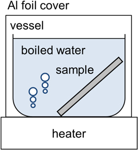
Fig. 1. Schematic image of heat treatment in liquid water at 90 °C.
Download figure:
Standard image High-resolution imageIn order to measure τeff precisely, we used a 9.35 GHz microwave transmittance measurement system, as previously reported. 36–38) The microwave propagated in waveguide tubes, which had a narrow gap for placing a sample, as shown in Fig. 2(a). The X–Y moving stage moved the sample to measure the spatial distribution of τeff. A continuous-wave (CW) laser diode light with a wavelength of 635 nm was introduced into the waveguide tube using an optical fiber connection, as shown in Figs. 2(a) and 2(b). The light intensity at the sample surface was set at 1.5 mW cm−2. The light penetration depth determined the photo-induced free carrier generation in the top 3 μm surface region of the silicon substrates. 39) The microwave transmitting the sample was rectified using a high-speed diode and analyzed to obtain the carrier density per unit area and τeff. For the investigation of the cut edge effects, a 2 mm wide light beam was formed by a black paper slit attached at the surface of the waveguide tube, as shown in Fig. 2(b). 26) The paper shaded the visible light completely, while being transparent to the 9.35 GHz microwave. The samples were cut into two half-moon-shaped pieces and set on the quartz plate, as shown in Figs. 2(b) and 2(c). τeff was measured as a function of the distance from the cut edge in the X-direction normal to the cut edge line, at which X was 0 cm when the central position of the light beam was positioned just at the cut edges of the sample. The spatial distribution of τeff in the X-direction for the initial 4 inch substrates, prior to making the cut edges, was also measured for reference.
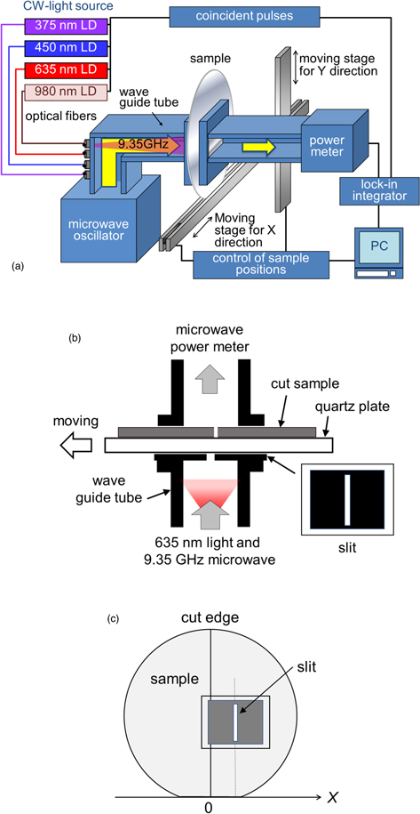
Fig. 2. Schematic of apparatus for a 9.35 GHz microwave transmittance measurement system for measuring τeff of sample wafers with 635 nm light illumination (a). Image of experimental measurement of τeff spatial distribution across the cut edge (b). Top view of the sample arrangement and definition of X-coordinates (c).
Download figure:
Standard image High-resolution image3. Results and discussion
Figure 3 shows τeff (solid circles) as a function of the distance X from the cut edge for (a) the as-cut sample and (b) the sample heat treated in liquid water for 2 h and then heat treated in air for 1 h. Figures 3(a) and 3(b) also show the calculated τeff (solid lines) as a function of X with different surface recombination velocities at the cut edges, as described in detail below. The as-cut sample had a high τeff ranging from 2.9 × 10⁻³ to 3.2 × 10⁻³ s in the region where X was larger than 0.5 cm, as shown in Fig. 3(a). Almost the same τeff distribution was observed for the 100 nm thick thermally grown SiO2-coated initial 4 inch samples prior to making the cut edges. The silicon surfaces were well passivated with the thermally grown SiO2 layers. When the experimental τeff is governed by the surface recombination velocity for both surfaces, Ssurface under the assumption of a high bulk lifetime of crystalline silicon, the experimental τeff gave Ssurface values ranging from 7.8 to 8.6 cm s−1. τeff gradually decreased as X approached the cut edge. Finally, τeff was 6.9 × 10⁻⁴ s at X of 0 cm, where the light beam illuminated the cut edge position. The decrease in τeff means that substantial photo-induced excess minority carrier annihilation occurred in the region about 0.5 cm from the cut edge, which is characterized by the minority carrier diffusion length, L
 where D is the minority hole carrier diffusion coefficient. L ranging from 0.19 to 0.20 cm for D of 12 cm2 s−1 and τeff ranging from 2.9 × 10⁻³ to 3.2 × 10⁻³ s indicate that photo-induced excess minority carriers generated in silicon in the region about 0.2 cm from the cut edge can laterally diffuse to the cut edge and be annihilated. After heat treatment in 90 °C liquid water for 2 h, followed by 300 °C for 1 h in air, τeff ranged from 7.6 × 10⁻⁴ to 9.4 × 10⁻⁴ s in the region far enough from the cut edge, as shown in Fig. 3(b). The assumption of a high enough bulk lifetime of crystalline silicon resulted in Ssurface ranging from 26 to 32 cm s−1. The slight increase in Ssurface is probably caused by charge accumulation at the SiO2 surfaces. Hot H2O molecules reacted with Si–O bonding and formed an Si–O–H negative ion, which applied the electrical field to the silicon surface and made the Fermi level at the silicon surface locate at the mid gap, which is much more active in carrier recombination according to the Shockley–Read–Hall theory
40) than the band flat condition of n-type silicon, whose Fermi level is located near the conduction band. In the case of the liquid water heat-treated sample, τeff also gradually decreased as X approached the cut edge. It decreased to 4.0 × 10⁻⁴ s at an X of 0 cm, which was almost half of the τeff value far from the cut edge. The reduction in τeff for the sample treated with liquid water was much smaller than a quarter for the as-cut sample. It suggests that the liquid water heat treatment achieved passivation of the cut edge region. It should also be noted that the width of the region for the decrease in τeff decreased to about 0.2 cm, which resulted from the decrease in L ranging from 0.095 to 0.11 cm for τeff ranging from 7.6 × 10⁻⁴ to 9.4 × 10⁻⁴ s.
where D is the minority hole carrier diffusion coefficient. L ranging from 0.19 to 0.20 cm for D of 12 cm2 s−1 and τeff ranging from 2.9 × 10⁻³ to 3.2 × 10⁻³ s indicate that photo-induced excess minority carriers generated in silicon in the region about 0.2 cm from the cut edge can laterally diffuse to the cut edge and be annihilated. After heat treatment in 90 °C liquid water for 2 h, followed by 300 °C for 1 h in air, τeff ranged from 7.6 × 10⁻⁴ to 9.4 × 10⁻⁴ s in the region far enough from the cut edge, as shown in Fig. 3(b). The assumption of a high enough bulk lifetime of crystalline silicon resulted in Ssurface ranging from 26 to 32 cm s−1. The slight increase in Ssurface is probably caused by charge accumulation at the SiO2 surfaces. Hot H2O molecules reacted with Si–O bonding and formed an Si–O–H negative ion, which applied the electrical field to the silicon surface and made the Fermi level at the silicon surface locate at the mid gap, which is much more active in carrier recombination according to the Shockley–Read–Hall theory
40) than the band flat condition of n-type silicon, whose Fermi level is located near the conduction band. In the case of the liquid water heat-treated sample, τeff also gradually decreased as X approached the cut edge. It decreased to 4.0 × 10⁻⁴ s at an X of 0 cm, which was almost half of the τeff value far from the cut edge. The reduction in τeff for the sample treated with liquid water was much smaller than a quarter for the as-cut sample. It suggests that the liquid water heat treatment achieved passivation of the cut edge region. It should also be noted that the width of the region for the decrease in τeff decreased to about 0.2 cm, which resulted from the decrease in L ranging from 0.095 to 0.11 cm for τeff ranging from 7.6 × 10⁻⁴ to 9.4 × 10⁻⁴ s.

Fig. 3. Experimental τeff (solid circles) and calculated τeff (solid lines) with different surface recombination velocities at the cut edge as a function of the distance X from the cut edge for (a) an as-cut sample, and (b) a sample heat treated in liquid water for 2 h and then heat treated in air for 1 h.
Download figure:
Standard image High-resolution imageTo investigate the decrease in τeff near the cut edges shown in Figs. 3(a) and 3(b), a numerical analysis program of carrier generation, diffusion, and annihilation using the finite differential element method was developed. 26,36,41) Under the present experimental conditions, the light beam was illuminated to the sample with a 2 mm width in the lateral X-direction and a 20 mm length in the vertical direction in the waveguide tube. Therefore, in the region of the sample, which the microwave transmitted in the waveguide tube, photo-induced carriers can be assumed to diffuse one-dimensionally in the lateral X-direction. The photo-induced carrier density per unit volume N(X) is given using the carrier diffusion model under a steady-state condition as

where D is the diffusion coefficient and g(X) is the carrier generation rate, which depends on X. The total carrier generation rate G(X) and the effective carrier lifetime τeff(X) for the light beam illuminated at the position X are given as

and

where d is the width of the light beam (2 mm) and W is the width of the waveguide tube (2 cm). The carrier lifetime τeff in Eq. (1) was used as the experimental values of 3.2 × 10⁻³ and 9.4 × 10⁻⁴ s, respectively, for the as-cut and liquid water heat-treated samples. The photo-induced carriers were annihilated at the cut edges. Therefore, we additionally set the induced carrier annihilation with a recombination velocity at the cut edges Scutedge as the boundary condition. When X is greater than d/2, no light illuminates the cut edge position, and the boundary condition is given as

On the other hand, when X is lower than d/2, the cut edge position is illuminated by the light. Therefore, the boundary condition is given as

where ΔX is the unit lattice distance for the calculation of finite elements.
The calculated τeff(X) with D of 12 cm2 s−1 and different Scutedge ranging from 20 to 200 000 cm s−1 as a function of X are shown in Figs. 3(a) and 3(b). In the case of the as-cut sample, the calculated τeff gradually decreased as X decreased to 0 cm because the photo-induced minority carriers laterally diffused and were annihilated at the cut edge, as shown in Fig. 3(a). The experimental τeff was well traced by the calculated curves, with Scutedge higher than 2000 cm s−1, which is the same order as that at the bare surface of crystalline silicon. This result shows that the decrease in the experimental τeff resulted from the decrease in the photo-induced minority carrier density, owing to the carrier annihilation at the cut edges with high Scutedge. τeff is not sensitive to Scutedge when it is higher than 2000 cm s−1. This is because the 0.2 cm light beam width always allows carrier generation at least 0.1 cm apart from the cut edge. In the case of the liquid water heat-treated sample, as shown in Fig. 3(b), the experimental τeff was also well traced by the calculated curves with Scutedge between 20 and 50 cm s−1, which was similar to the Ssurface of the sample treated with liquid water. The liquid water heat treatment markedly decreased Scutedge and allowed a high density of photo-induced minority carriers near the cut edge. The decreases in the experimental τeff near the cut edges shown in Figs. 3(a) and 3(b) can be explained by the simple model calculation of carrier diffusion in the lateral direction and the annihilation by the recombination defect states at the cut edges. Furthermore, the low Scutedge values shown in Fig. 3(b) suggest that the cut edges were well passivated by the present condition of liquid water heat treatment.
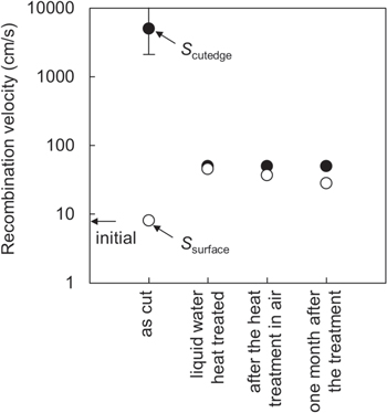
Figure 4 shows the changes in the numerically analyzed Ssurface (open circles) and Scutedge (solid circles) with the process sequence for the samples. The as-cut sample shows a high Scutedge of higher than 2000 cm s−1 because the mechanical cutting markedly increased the carrier recombination defect states at the cut edge region. On the other hand, the Ssurface of the as-cut sample maintained the 8 cm s−1 initial value of the samples prior to making the cut edges. The surfaces were well passivated by the thermally grown SiO2 layers. The Scutedge markedly decreased to 50 cm s−1 for the sample just after the liquid water heat treatment at 90 °C for 2 h. The passivation of cut edges was achieved at this stage by the formation of thin oxide layers. The liquid water heat treatment also increased Ssurface to 46 cm s−1, probably due to the field-induced depletion effect caused by negatively charging up the SiO2 surface. After the heat treatment in air at 300 °C for 1 h, Scutedge did not change from 50 cm s−1, while Ssurface slightly decreased to 37 cm s−1. In addition, by keeping the heat-treated samples in air atmosphere for one month at a temperature of 20 °C and a humidity of 50%, Ssurface further decreased to 28 cm s−1. These results show that the present heat treatment in liquid water has the capability of stable passivation of the silicon cut edges with low recombination defect states. It will be valuable to carry out further investigation of the optimum conditions of the liquid water heat treatment to achieve a higher and more stable τeff. In addition, it is expected that the difference in cut surface morphology will cause variations in the τeff obtained by the liquid water heat treatment. The quality of the silicon substrates also affected the passivation results. To apply the present passivation method in industrial production, further investigation will also be required to establish the optimizing conditions for uniform and stable passivation for large semiconductor wafers.
Fig. 4. Changes in numerically analyzed Ssurface (open circles) and Scutedge (solid circles) with the process sequence for the samples. The arrow shows the initial Ssurface of the samples prior to making cut edges.
Download figure:
Standard image High-resolution image
4. Conclusions
We report on the passivation of cut edges and surfaces of n-type single-crystalline silicon substrates with an orientation of (100) and a thickness of 500 μm coated with 100 nm thick thermally grown SiO2 layers. The substrates were cleaved normal to the orientation flat with the (110) direction to make two half-moon-shaped pieces. Then, they were heated in liquid water at 90 °C for 2 h followed by heating in an air atmosphere at 300 °C for 1 h. The distributions of the photo-induced effective minority carrier lifetime τeff normal to the cut edge line were measured by a 9.35 GHz microwave transmittance measurement system under 635 nm CW light illumination. The cleaved edge markedly decreased the τeff to 6.9 × 10⁻⁴ s, which was 0.22 times the initial value of 3.2 × 10⁻³ s, which the region 0.5 cm away from the edge maintained. The present passivation treatment improved the reduction of τeff to 0.43, with τeff values of 4.0 × 10⁻⁴ s at the edge and 9.4 × 10⁻⁴ s at a distance of 0.2 cm away from the edge. The numerical analysis with a simple model of carrier diffusion in the lateral direction and annihilation at the cut edges resulted in the recombination velocity at the cut edge Scutedge, which was initially higher than 2000 cm s−1, being decreased to 50 cm s−1 by the present treatment, while the recombination velocity at the sample surface Ssurface was increased from 8 (initial) to 46 cm s−1, probably due to the field-induced depletion effect. The passivation was maintained for at least one month and Ssurface further decreased to 28 cm s−1. The present results indicate that the treatment in liquid water has the capability of simple passivation at a low temperature and low-cost for the cut edges as well as the bare surfaces of crystalline silicon. Although further investigation is required, the present method will be useful for fabricating high-performance photo-sensors and photovoltaic devices.
Acknowledgments
This work was partially supported by Grants-in-Aid for Scientific Research, KAKENHI 21K04134 and 22K04180 from the Japan Society for the Promotion of Science.