
Abstract
Graphene is well-known as a material with extremely high carrier mobility, although its electrical properties can be changed into those of a highly insulating thin film by a fluorination treatment (fluorographene). Taking advantage of this property, a flexible nonvolatile memory using fluorographene as a charge trapping layer has been proposed. However, the mechanism of charge trapping on fluorographene is not yet fully understood. In this paper, we fabricated fluorographene and analyzed it by X-ray photoelectron spectroscopy and Raman spectroscopy. Furthermore, metal–insulator–semiconductor (MIS) capacitors inserted with fluorographene were fabricated and evaluated electrically. As a result, a large flat-band voltage shift was observed even though the fluorine concentration (C–F bonding ratio) was saturated at around 14%. Furthermore, the charge centroid of the MIS capacitor with fluorographene coincides with the location of the fluorographene. These results indicate that fluorographene can capture injected charges and is a candidate for use in nonvolatile memory with two-dimensional materials.
Export citation and abstract BibTeX RIS
1. Introduction
In recent years, the amount of generated data has continued to grow each year, and it is predicted that 181 ZB of data will be generated in 2025. 1) To store and use such massive amounts of data effectively, high-density and high-capacity storage from the edge to the cloud are desperately required. 2) In particular, flexible devices will become important technologies for the evolution of Internet of Things equipment such as wearable devices. That is why we are focusing on flexible memory using two-dimensional materials. Graphene, which is one such two-dimensional (2D) material, has attracted much attention due to its unique properties, and it is expected to be applied in next-generation nanoelectronics. 3–8) In general, graphene is investigated as a transistor channel in nanoribbon structures, since they have high carrier mobility. 9–11) However, since graphene is a conductive material, it is difficult to use it as a charge trapping layer for nonvolatile memory. To solve this issue, a charge trapping memory structure using graphene oxide has been proposed. However, graphene oxide has low thermal stability. 12–14) Among several other memory devices using ultra-thin 2D materials, 15,16) we focus on fluorographene in this study. Fluorographene has high thermal stability, and its electrical conductivity can be varied by changing the ratio of carbon to fluorine. 14,17) Taking advantage of this property, a flexible nonvolatile memory using fluorographene as a charge trapping layer has been proposed and demonstrated a threshold voltage shift and/or a flat-band voltage shift by electron injection. 18–21) However, it is not clear whether fluorographene itself plays a role in capturing carriers. Furthermore, it is a concern that the graphene may suffer damage during the fluorination process, which could affect device operation. While most previous research has focused on electrical properties, detailed investigations about the properties of fluorographene are critical to the fabrication of these devices. Therefore, in this paper, we prepare fluorographene and investigate its properties from a physical and electrical point of view. In particular, using fabricated devices, it is clarified whether fluorographene can really function as a charge trapping layer.
2. Experimental details
Graphene is grown on Cu foil using a thermal chemical vapor deposition (CVD) method. Several fluorination processes for graphene have been reported in the literature. 19,22–26) In this study, fluorination of graphene was carried out using CF4 plasma treatment in conventional reactive ion etching (RIE) equipment, 19) which is advantageous in terms of uniformity, CMOS-process compatibility, and treatment for large-area samples. To protect the graphene from high-energy ions, it was set upside down in the RIE chamber. The fluorographene was transferred onto a SiO2/Si substrate after selectively etching Cu foil. In this paper, the tunnel oxide is 8 nm SiO2 film grown by thermal oxidation. After transferring the fluorographene, Al2O3 films were deposited as a 10 nm blocking oxide film by atomic-layer deposition (ALD). Finally, Al electrodes were deposited on the top and bottom of the device by vapor deposition. Figure 1 shows the process flow and process conditions.
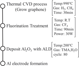
Fig. 1. Process flow and process conditions for device fabrication.
Download figure:
Standard image High-resolution image3. Results and discussion
The physical properties of fluorographene were investigated using X-ray photoelectron spectroscopy (XPS) and Raman spectroscopy. Figure 2 shows typical high-resolution XPS spectra of C1s with fluorination treatment times of 15 min and 90 min. The fluorocarbon (i.e. C–F, CHF and CFx bonds) can be deconvoluted and identified from the respective C1s spectra. This means that the graphene is fluorinated and C–F related bonds are formed. These spectra are identical to those in previous reports. 26,27) Figure 3 shows the relationship between the C–F binding ratio and fluorination treatment time. It is possible to calculate the C–F binding ratio from the areas of the deconvoluted spectra using Eq. (1)

With fluorination treatment, the proportion of C–F bonds saturates at about 14%. This means that the graphene is not entirely fluorinated, only partially fluorinated. In this study, the fluorination process was performed prior to graphene transferring to the tunnel oxides. On the other hand, we also tried performing fluorination after transferring graphene to the tunnel oxides. In this case, the amount of C–F bonding is estimated to be around 4%, and almost all the fluorine was introduced into the tunnel oxide film. It has been already reported that incorporation of large amounts of fluorine deteriorates the quality of the tunnel oxide. 19) Therefore, fluorination prior to graphene transfer has been adopted in this study.
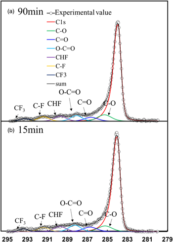
Fig. 2. (Color online) Typical C1s spectra measured by high-resolution XPS: fluorination treatment time of (a) 90 min and (b) 15 min. Fluorocarbon can be seen by deconvolution of the C1s spectra.
Download figure:
Standard image High-resolution image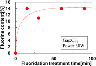
Fig. 3. (Color online) Relation between fluorination treatment time and the C–F binding ratio.
Download figure:
Standard image High-resolution imageFigure 4 shows the Raman spectra of graphene and fluorographene on Cu foils. The G-band (≅1650 cm−1) and 2D-band (≅2700 cm−1) spectra, which are typical Raman spectra of graphene, 28) can be observed in each specimen even after fluorination. Furthermore, as the fluorination time is increased, the D-band (≅1350 cm−1) spectrum is observed. The D-band spectrum is attributed to sp2 defects. 29) Therefore, these results imply that these defects are generated during the fluorination process.
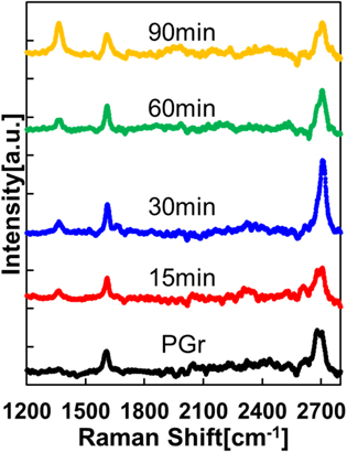
Fig. 4. (Color online) Raman spectra of graphene and fluorographene on Cu foil.
Download figure:
Standard image High-resolution imageFigure 5(a) shows the calculated I2D/IG of graphene and fluorographene on Cu foils. The I2D/IG ratio is used to evaluate the number of graphene layers. In this case, the I2D/IG ratios are between 1.5 and 2.0, indicating that graphene and fluorographene are monolayers. Figure 5(b) shows the intensity of the D-band spectra and the IG/ID ratio for different fluorination times. The number of defects can be evaluated qualitatively by the IG/ID ratio. Note that the intensity of the D-band spectra becomes stronger with increasing fluorination time. Furthermore, the IG/ID ratio becomes lower, indicating that the number of defects is increasing. The results in Fig. 5 imply that the graphene is damaged during the fluorination process but maintains the graphene structure.

Fig. 5. (Color online) Relation between the Raman shift and fluorination treatment time: (a) I2D/IG ratio, (b) intensity of D-band spectra and IG/ID ratio. (IG, ID and I2D are represented as the intensities of G-band, D-band and 2D-band spectrum, respectively.)
Download figure:
Standard image High-resolution imageFigure 6 shows the Raman spectra of graphene and fluorographene after transfer. Figure 6(a) shows the spectrum of graphene transferred to SiO2, where the G-band and 2D-band spectra are observed clearly. Figure 6(b) shows the spectrum of fluorographene transferred to SiO2. The G-band and 2D-band spectra can also be observed, while the D-band spectrum due to the fluorination process is confirmed. This is consistent with the Raman spectra of graphene on Cu foils. Figure 6(c) shows the result after deposition of Al2O3 onto the transferred fluorographene. Note that the G-band and 2D-band spectra are clearly seen, indicating that fluorographene remained after Al2O3 deposition. In Fig. 6(c), the intensity of the D-band spectrum is suppressed compared with that before Al2O3 deposition [Fig. 6(b)]. It is inferred that that oxygen used during the Al2O3 ALD process partially terminated the defects in the graphene by forming graphene oxide.
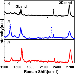
Fig. 6. (Color online) Raman spectra of graphene after transfer: (a) pure graphene on SiO2, (b) fluorographene on SiO2, (c) fluorographene beneath an Al2O3 blocking layer.
Download figure:
Standard image High-resolution imageMetal–insulator–semiconductor (MIS) capacitors were fabricated using the process shown in Fig. 1 and their electrical characteristics evaluated. The fluorographene used in the MIS capacitors was fluorinated for 90 min. Figure 7 shows the device structure used in this study and the cross-sectional transmission electron microscope (TEM) images.
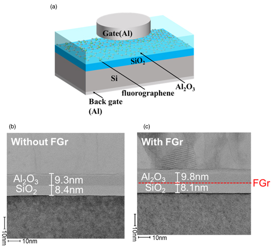
Fig. 7. (Color online) MIS capacitor fabricated in this study: (a) schematic diagram of the MIS capacitor, (b) cross-sectional TEM images for the device without fluorographene and (c) cross-sectional TEM images for the device with fluorographene.
Download figure:
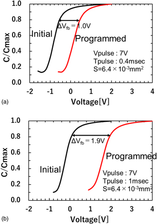
Standard image High-resolution imageFigure 8 shows the C–V curves of the device with and without fluorographene. In both cases, the C–V curves shift to a positive direction after a positive pulse voltage is applied to the gate electrodes. A flat-band voltage shift (ΔVFB) of 1.0 V is observed in the MIS capacitor without fluorographene, as shown in Fig. 8(a), suggesting that injected electrons are captured in the Al2O3 layer. On the other hand, a larger ΔVFB of 1.9 V is observed in the device with fluorographene, as shown in Fig. 8(b). As can be seen in Figs. 7(b) and 7(c), the thicknesses of the tunnel oxide (SiO2) and the blocking layer (Al2O3) are almost the same in both devices. Therefore, the results in Fig. 8 indicate an improvement in the electron trapping property by the insertion of fluorographene. This result is consistent with the results of previous studies. 19) To understand this in more detail, the centroids of captured electrons are evaluated. 30) The charge centroid is the distance from the electrode, which can be calculated from Eq. (2)

where ε0 is dielectric constant of a vacuum, ε is dielectric constant of Al2O3, Qtrap is the amount of injected charge evaluated during application of the pulse voltage and ΔVFB is the flat-band voltage shift which is obtained from the C–V measurement. Table I shows the charge centroids for the devices with and without fluorographene. In the case of the device without fluorographene, the charge centroid is calculated to be 2.41 nm. According to the TEM image, as shown in Fig. 7(b), it can be recognized that the charge centroid is located at the Al2O3 blocking layer. On the other hand, the charge centroid for the device with fluorographene is calculated to be 10.3 nm. This result indicates that the charge centroid becomes deeper due to the insertion of fluorographene. Furthermore, it should be noted that the charge centroid is located almost at the interface between the Al2O3 blocking layer and the tunnel oxide film, which coincides with the position of the inserted fluorographene. As explained in Fig. 1, since the tunnel oxide films are grown by thermal oxidation, it is inferred that the quality and the reliability of the tunnel oxide films are acceptable. These results suggest that the electron trapping efficiency is improved by the insertion of fluorographene and fluorographene is promising for use as an ultra-thin charge trapping layer.
Fig. 8. (Color online) C–V characteristics of initial and programmed devices: (a) without fluorographene, (b) with fluorographene. Note that a shift about two times larger can be observed with insertion of fluorographene.
Download figure:
Standard image High-resolution image
The graphene used in this study was deposited by thermal CVD, so it is polycrystalline with grain boundaries. 31–33) Since the C–F binding ratio is saturated at about 14%, as shown in Fig. 3, it is inferred that fluorine atoms bind at these grain boundaries. Fluorinated grain boundaries show an insulating property. We have two hypotheses for the electron trapping mechanism. One is that the fluorinated grain boundaries work as energy barriers and charges are trapped in graphene islands. This model has been proposed for the floating gate type memory cell with graphene oxide [9]. The other is that the charges are trapped in the C–F bonds directly as in charge trap type memory cells.
Table I. Parameters obtained from experiments and calculation results for the charge centroid.
| ΔV FB [V] | Q trap [pC] | Zeff [nm] | |
|---|---|---|---|
| Without fluorographene | 1.0 | 225 | 2.41 |
| With fluorographene | 1.9 | 128 | 10.3 |
The actual mechanism of charge trapping has not yet been clarified and more investigations are required to understand the detailed trapping mechanism.
4. Conclusion
Our research was aimed at clarifying the charge trapping characteristics of fluorographene for nonvolatile memory applications. We found that the C–F binding ratio saturates at about 14%. We were also able to confirm by Raman spectroscopy that fluorographene remains after deposition of a blocking film (ALD Al2O3). ΔVFB was about doubled by the insertion of fluorographene. The estimated charge centroid coincides with the location of the inserted fluorographene. These experimental results show that although fluorographene is an ultra-thin material it can function as a charge trapping layer. In conclusion, the electron trapping efficiency is improved by the insertion of fluorographene and fluorographene is promising for use in an ultra-thin charge trapping layer.
Acknowledgments
This work was partly supported by Tokyo City University Interdisciplinary Research Center for Nano Science and Technology for instrumental analysis. This work was partially supported by Grant in Aid for Scientific Research (No. JP22K04743).