

Abstract
We report the growth of α-Ga2O3 on m-plane α-Al2O3 by conventional plasma-assisted molecular-beam epitaxy and In-mediated metal–oxide-catalyzed epitaxy (MOCATAXY). We report a growth rate diagram for α-Ga2O3( ), and observe (i) a growth rate increase, (ii) an expanded growth window, and (iii) reduced out-of-plane mosaic spread when MOCATAXY is employed for the growth of α-Ga2O3. Through the use of In-mediated catalysis, growth rates over 0.2 μm h−1 and rocking curves with full width at half maxima of Δω ≈ 0.45° are achieved. Faceting is observed along the α-Ga2O3 film surface and explored through scanning transmission electron microscopy.
Export citation and abstract BibTeX RIS
Corrections were made to this article on 30 May 2023. "out-of-lane" in the abstract was corrected to "out-of-plane".
1. Introduction
Over the past decade, Ga2O3 has gained much attention as a wide-band gap semiconductor. Monoclinic β-Ga2O3 possesses an ultra-wide bang gap of ∼4.7 eV, 1) and it has been the most studied phase owing to its thermal stability and the availability of large-area, native, semi-insulating, and conductive substrates. 2,3) To further increase its band gap β-Ga2O3 can be alloyed with Al to form β-(Al,Ga)2O3, but achieving a high Al content has remained challenging due to the tendency to have phase segregation. 4) In contrast, α-(Al,Ga)2O3 becomes more stable as the Al is increased because the crystal is isostructural with the α-Al2O3 substrate and the lattice mismatch is reduced as the Al concentration is increased. 5) This has enabled the entire compositional range of α-(Al,Ga)2O3 to be readily achieved, 5,6) and it has enabled band gaps exceeding those of AlN, BN, or diamond. 7,8)
With the recent advances enabling α-Ga2O3 to remain stable during high-temperature anneals, 9) the next challenge is to achieve electrical conductivity. To date, conductivity in α-Ga2O3 has been achieved by chemical vapor deposition (CVD), 10,11) but has remained elusive for films grown by molecular-beam epitaxy (MBE). Additionally, conductive β-Ga2O3 films grown by MBE on α-Al2O3 have yet to be achieved. 7) While the exact reasons these films remain insulating are unknown, the thermodynamics during MBE growth and the low formation energy of defects may cause these Ga2O3 films on Al2O3 to be insulating.
Multiple compensating point defects (e.g. cation vacancies, oxygen vacancies, donor impurities 12,13)) and extended crystallographic defects (e.g. rotational domains and threading dislocations 14)) occur within the Ga2O3 films grown on sapphire. Reasons for the emergence of these defects include the lattice mismatch between the film and the substrate, 14) and the growth regime in which the films are grown. 12,13,15) For example, Ga vacancies (VGa) may act as compensating acceptors for introduced n-type dopants in grown Ga2O3 thin films. 15) O-rich growth environments are likely to generate a significant amount of VGa (due to their low formation energy) whereas Ga-rich growth environments are found to significantly suppress the formation of VGa (due to their high formation energy). 13) Thus, the growth of Ga2O3 in the highly Ga-rich regime—accessed by new epitaxial growth concepts 16,17)—may improve the transport properties of Ga2O3 thin films since the Ga-rich growth regimes lead to higher VGa formation energies, resulting in lower VGa densities within the Ga2O3 layers.
One approach to address these issues is through the use of metal–oxide-catalyzed epitaxy (MOCATAXY). 18) This is a growth process where a catalytic element (e.g. In) is introduced to the growth system and results in metal-exchange catalysis. 19) This growth mode has been observed for β-(Al,Ga)2O3 on different substrates and surface orientations, as well as for different epitaxial growth techniques. 20–24)
Many benefits arise from using MOCATAXY during the growth of Ga2O3. For example: (i) it can improve the surface morphologies of β-Ga2O3-based films.
21) (ii) The synthesis of Ga2O3 can occur in previously inaccessible kinetic and thermodynamic growth regimes (e.g. in highly metal-rich regimes) which can be beneficial for the suppression of undesired point (such as VGa) defects in Ga2O3.
12,13,19) (iii) The formation of thermodynamically unstable Ga2O3 phases becomes energetically favorable,
16,19,24) e.g. the formation of the  /κ-phase of Ga2O3, which has enabled novel /κ-Ga2O3-based heterostructures.
23) (iv) The growth rate (Γ), possible growth temperatures (TG), and crystalline quality of β-(Al,Ga)2O3-based thin films can be vastly enhanced.
18)
/κ-phase of Ga2O3, which has enabled novel /κ-Ga2O3-based heterostructures.
23) (iv) The growth rate (Γ), possible growth temperatures (TG), and crystalline quality of β-(Al,Ga)2O3-based thin films can be vastly enhanced.
18)
In this work, we introduce the growth of α-Ga2O3 by MOCATAXY, resulting in an expansion of the α-Ga2O3 growth window combined with an increased Γ and an improvement in its out-of-plane mosaic spread. It is the first demonstration of a catalytic growth process during the growth of α-Ga2O3.
2. Experimental
Samples were grown in a Veeco GEN930 plasma MBE system with standard Ga and In effusion cells. For all samples, the substrates were cleaned in acetone and isopropanol for 10 min and the α-Ga2O3 samples were grown for 60 min. The growth temperature (TG) was measured by a thermocouple located within the substrate heater. The Ga flux (ϕGa) and In flux (ϕIn) were monitored by beam equivalent pressure (BEP) chamber readings. For conventional MBE and MOCATAXY, the O2 flux (ϕO) was measured in standard cubic centimeters per min (SCCM) and a radio-frequency plasma power of 250 W was employed during all growths. To convert the measured values of ϕGa (BEP), ϕIn (BEP), and ϕO (SCCM) into units of nm−2 s−1 conversion factors are taken from Ref. 25. Note, when using In-mediated catalysis, the available ϕO for Ga to Ga2O3 oxidation is about 2.8 times larger than for Ga oxidation in the absence of In. 16,19)
For samples grown by conventional MBE and MOCATAXY, the impact of ϕGa and TG is studied. In the case of MOCATAXY growth, the impact of ϕIn is also investigated. All the growth parameters used in this work are collected in Table I. For scanning transmission electron microscopy (STEM), samples were prepared using a Thermo Fisher Helios G4 UX Focused Ion Beam with a final milling step of 5 keV to minimize damage. Carbon and Au–Pd layers were sputtered to reduce charging during sample preparation. Carbon and platinum protective layers were also deposited to minimize ion-beam damage. STEM measurements were taken with an aberration-corrected Thermo Fisher Spectra 300 CFEG operated at 300 keV.
Table I. Collected growth parameters used in this work, values of ϕGa, ϕIn, ϕO, and TG, for samples grown by conventional MBE and MOCATAX are listed. The conversion for ϕGa and ϕIn from BEP to  to nm−2 s−1 are ϕGa = 2.5 × 10⁻⁸ Torr
 and
and  , respectively.
| Growth parameters | Conventional MBE | MOCATAXY |
|---|---|---|
| ϕGa (nm−2 s−1) | 0.8–2.0 | 1.1–5.5 |
| ϕIn (nm−2 s−1) | 0 | 2.6–2.8 |
| ϕO (SCCM) | 1.4 | 0.7–1.0 |
| ϕO (nm−2 s−1) | 2.2 | 3.2–4.6 |
| TG (°C) | 640–800 | 680 |
3. Results and discussion
Figure 1 shows the growth-rate-diagram of α-Ga2O3( ) grown on α-Al2O3(
 ) by conventional MBE (the gray shaded area) and MOCATAXY (the purple shaded area). For conventionally grown samples two distinct growth regimes are observed: (i) the O-rich regime where O adsorbates are in excess over Ga adsorbates (i.e. the Ga flux limited regime), and (ii) the Γ-plateau regime (i.e. the Ga2O desorption limited regime). The O-rich regime is characterized by an increasing Γ with increasing ϕGa, whereas the plateau regime is characterized by a constant Γ, being independent of ϕGa. Within this regime, however, Γ may decrease with increasing TG (see inset in Fig. 1) as the desorption of the volatile suboxide Ga2O becomes thermally more active.
26) The data in the inset of Fig. 1 plots Γ as a function of TG for (i) α-Ga2O3 grown the O-rich regime and (ii) α-Ga2O3 grown in the Γ-plateau regime.
) by conventional MBE (the gray shaded area) and MOCATAXY (the purple shaded area). For conventionally grown samples two distinct growth regimes are observed: (i) the O-rich regime where O adsorbates are in excess over Ga adsorbates (i.e. the Ga flux limited regime), and (ii) the Γ-plateau regime (i.e. the Ga2O desorption limited regime). The O-rich regime is characterized by an increasing Γ with increasing ϕGa, whereas the plateau regime is characterized by a constant Γ, being independent of ϕGa. Within this regime, however, Γ may decrease with increasing TG (see inset in Fig. 1) as the desorption of the volatile suboxide Ga2O becomes thermally more active.
26) The data in the inset of Fig. 1 plots Γ as a function of TG for (i) α-Ga2O3 grown the O-rich regime and (ii) α-Ga2O3 grown in the Γ-plateau regime.
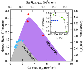
Fig. 1. (Color online) Growth-rate-diagram of α-Ga2O3( ) grown on α-Al2O3(
 ). The growth rate Γ as a function of ϕGa at TG = 680 °C is plotted for the growth by conventional MBE (blue triangles) and MOCATAXY (red stars). The Γ-data is fit by a Γ-model taken from Ref. 28. The gray shaded region shows the parameter space under which the formation of α-Ga2O3 by conventional MBE may occur. The purple shaded area depicts the growth regime of α-Ga2O3 assisted by MOCATAXY. Both fitted data sets were obtained at constant TG and ϕO (values given in Table I). Inset: Γ as a function of TG at two different fluxes of (i) ϕGa = 0.9 nm−2 s−1 (the O-rich regime, solid squares) and (ii) ϕGa = 1.6 nm−2 s−1 (the Γ-plateau regime, solid discs). A growth-rate-diagram of α-Ga2O3 as a function of ϕO is given in Ref. 27.
Download figure:
Standard image High-resolution imageTo expand the accessible growth window of α-Ga2O3 to higher ϕGa and to higher TG, combined with increased Γ and improved crystalline quality, In-mediated catalysis was employed in the formation of α-Ga2O3.
19) The red stars in Fig. 1 show the resulting Γ as a function of ϕGa at constant TG. The gray shaded and purple shaded areas in Fig. 1 depict model-based descriptions of Γ for α-Ga2O3 grown by conventional MBE and MOCATAXY, respectively. The maximum Γ obtained for each growth technique is  and
and  , respectively. Using MOCATAXY, a more than 2-times increase in Γ for α-Ga2O3 at given growth conditions, as well as a shift far into the adsorption-controlled regime (i.e. far into the Ga-rich flux regime) is observed. This direct comparison between the two growth types clearly shows the expanded growth window made possible with MOCATAXY, for example, enabling
  for α-Ga2O3 at ϕGa = 5.5 nm−2 s−1. In contrast, at these growth conditions, no growth of α-Ga2O3 is obtained by conventional MBE. The catalytic effect on Γ of α-Ga2O3 is modeled as a function of ϕO within the supplemental section.
27) We note that the depicted models use arbitrary kinetic parameters, based on kinetic parameters extracted for the growth ofβ-Ga2O3.
28)
for α-Ga2O3 at ϕGa = 5.5 nm−2 s−1. In contrast, at these growth conditions, no growth of α-Ga2O3 is obtained by conventional MBE. The catalytic effect on Γ of α-Ga2O3 is modeled as a function of ϕO within the supplemental section.
27) We note that the depicted models use arbitrary kinetic parameters, based on kinetic parameters extracted for the growth ofβ-Ga2O3.
28)
To describe the growth of α-Ga2O3 by MOCATAXY, ϕO is scaled by a factor of 2.8 compared with the growth of α-Ga2O3 by conventional MBE. This additional O comes from the catalytic nature of In forming a catalytic adlayer (A) with O adsorbates, e.g. A= In–O, which provides more active O for the Ga to α-Ga2O3 oxidation. In other words, A increases the reaction probability of Ga with O on the respective growth surface, facilitating the formation of the final Ga2O3 compound at much higher ϕGa and TG, which enables excellent crystal quality. 16,19) We further note that the same factor of 2.8 was needed for modeling the MOCATAXY growth of β-Ga2O3 on different substrates and different surface orientations. 16,19) We note, however, that for a quantitative extraction of all kinetic growth parameters more Γ-studies of α-Ga2O3 are needed and are beyond the scope of this work. Nevertheless, the models help validate the Γ-data and provide insight into the growth regimes and growth mechanisms of α-Ga2O3. For example, once ϕGa exceeds the active O flux, i.e. ϕGa > ϕO, the growth will enter the Ga-rich regime and Γ will start to decrease, as shown by the gray shaded area in Fig. 1. Thus, this is the first direct indication that the growth of α-Ga2O3 is limited by the formation and subsequent desorption of Ga2O, like what is observed for β-Ga2O3 grown by conventional MBE. 28)
Figure 2 directly compares the impact of both MBE growth techniques on the structural quality of the epitaxially grown films. In Fig. 2 (a), 2θ-ω XRD scans of two selected α-Ga2O3 films are shown, one grown by conventional MBE (depicted as the blue trace) and one grown by MOCATAXY (depicted as the red trace). The reflections of the films coincide with the α-Ga2O3
 peak. This, along with the absence of other diffraction peaks, indicates phase-pure α-Ga2O3(10
  0) with In incorporation of <1% in the grown α-Ga2O3 layers, similar to what is observed for β-(Al,Ga)2O3 grown by MOCATAXY.
18) Figures 2(b) and 2(c) plot transverse scans (rocking curves) for the conventional MBE and MOCATXY grown α-Ga2O3 samples as plotted in Fig. 2(a). The rocking curves are measured across the symmetric
0) with In incorporation of <1% in the grown α-Ga2O3 layers, similar to what is observed for β-(Al,Ga)2O3 grown by MOCATAXY.
18) Figures 2(b) and 2(c) plot transverse scans (rocking curves) for the conventional MBE and MOCATXY grown α-Ga2O3 samples as plotted in Fig. 2(a). The rocking curves are measured across the symmetric  peak. The full width at half maxima (FWHM) of ω quantifies the out-of-plane mosaic spread of the α-Ga2O3 film. For conventionally grown films the out-of-plane crystal distribution is Δω ≈ 0.55° and for MOCATAXY grown films it is Δω ≈ 0.45°. The film thicknesses d of the conventionally and MOCATAXY grown films are d = 73 nm and d = 127 nm, respectively. Jinno et al. reported that α-Ga2O3 films are fully relaxed for d > 60 nm.
5) Since lattice mismatch and relaxation are not impacted by MOCATAXY, it is noteworthy that despite the MOCATAXY film being thicker, Δω is substantially smaller compared to what is obtained by conventional growth. The same MOCATAXY grown sample shown here is studied by STEM in Fig. 4.
peak. The full width at half maxima (FWHM) of ω quantifies the out-of-plane mosaic spread of the α-Ga2O3 film. For conventionally grown films the out-of-plane crystal distribution is Δω ≈ 0.55° and for MOCATAXY grown films it is Δω ≈ 0.45°. The film thicknesses d of the conventionally and MOCATAXY grown films are d = 73 nm and d = 127 nm, respectively. Jinno et al. reported that α-Ga2O3 films are fully relaxed for d > 60 nm.
5) Since lattice mismatch and relaxation are not impacted by MOCATAXY, it is noteworthy that despite the MOCATAXY film being thicker, Δω is substantially smaller compared to what is obtained by conventional growth. The same MOCATAXY grown sample shown here is studied by STEM in Fig. 4.
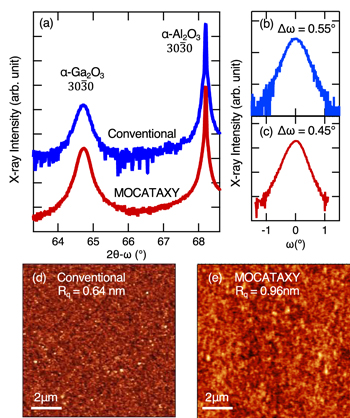
Fig. 2. (Color online) (a) Longitudinal XRD scans of optimized α-Ga2O3 films are shown. The reflections of the films coincide with the α-Ga2O3
 phase grown by conventional MBE (the blue trace) and MOCATAXY (the red trace). The used growth parameters were ϕGa = 2.9 nm−2 s−1,
  , and TG = 750 °C (conventional MBE), and ϕGa = 2.9 nm−2 s−1, ϕIn = 2.8 nm−2 s−1, ϕO = 0.7 SCCM
  , and TG = 680 °C (MOCATAXY). (b) and (c) Transverse XRD scans across the
  peak with their FWHM of Δω = 0.55° (conventionally MBE-grown) and Δω = 0.45° (MOCATAXY grown) are shown. These obtained Δω are depicted in Fig. 3 at given ϕGa and TG. (d) and (e) Display surface morphologies obtained from 10 × 10 μm AFM scans for α-Ga2O3(
 ) surfaces grown by conventional MBE and MOCATAXY, respectively. Growth conditions for the samples plotted in (d) and (e) are the same as for the ones plotted in panels (a)–(c), except a slightly lower TG = 730 °C is used for the conventionally grown sample and a slightly higher supplied ϕO = 1.0 SCCM for the MOCATAXY grown film. This resulted in Δω = 0.61° and
  for the conventionally grown sample, and Δω = 0.48° and Γ > 3.0 nm min−1 for the MOCATAXY grown sample.
Download figure:
Standard image High-resolution imageSurface morphologies and root mean square roughnesses (Rq) are measured by AFM and depicted in Figs. 2(d) and 2(e). The best surface roughness for conventionally grown α-Ga2O3 with d = 66 nm is Rq = 0.64 nm, while the smoothest one for MOCATAXY grown samples with d ∼ 270 nm has an Rq = 0.94 nm. The larger surface roughness for the MOCATAXY grown sample is likely due to facetting on the top surface of the α-Ga2O3 thin film [see Fig. 4(a)]. We speculate that In does not only act as a catalyst but also acts as a surface active agent (surfactant) for the growth α-Ga2O3 thin films. It is widely understood that In can act as a surfactant for the epitaxial growth of GaN-based films, 29) and has also been observed during the growth of β-Ga2O3 21) and β-(Al,Ga)2O3. 18) Depending on the growth conditions and growth surface, which can affect the surface diffusion kinetics, surface chemical potentials, and the assessed growth mode, the suppression of facetting may be accomplished through the use of optimized conditions, while using In as a surfactant, enabling a modification in the surface free energies of the growing α-Ga2O3 thin film and a change in its growth mode. 18,21,30,31) However, surfactant-induced morphological phase-transitions from two-dimensional (2D) layer growth to three-dimensional (3D) island growth have also been observed during MBE growth. 32) We believe that a similar effect occurs for the α-Ga2O3 surfaces studied here when In may act as an (anti)surfactant during the growth of these films. Note, we have not fully explored all growth regimes made accessible through MOCATAXY in this study. Further studies may lead to additional improvements in the crystalline quality and surface morphologies of the α-Ga2O3 thin films.
In Figs. 3(a) and 3(b), the impact of ϕGa and TG, respectively, on Δω for samples grown by conventional MBE in the O-rich regime (blue squares) and in the Γ-plateau regime (green circles), as well as for samples grown by MOCATAXY (red stars), are shown. XRD data and Δω are obtained by the same methods as described above for Fig. 2. Within the O-rich regime at TG = 640 ◦C, a large Δω is observed, Fig. 3(a). At higher growth temperatures (i.e. TG ≥ 660 ◦C), Δω are similar (or slightly improving) with increasing temperature, regardless of growth regime. We speculate that the reason the crystal quality improves with TG, is that there is an increase in the kinetic energy and a subsequent increase in the diffusion length of the adsorbates, allowing the Ga and O to reach the proper lattice site. However, if TG is increased too much, a decrease in the surface lifetime of Ga adsorbates may occur, resulting in a reduction in the crystalline quality of the growing thin films. Using MOCATAXY in the Ga-rich regime with a fixed TG, excess Ga may now reduce the needed surface diffusion length, improving the crystalline quality in the obtained α-Ga2O3 layers. More studies to separate the effects of ϕGa and TG on Δω need to be performed, but to the best of our knowledge, the obtained Δω values are the lowest reported in the literature for α-Ga2O3 grown on α-Al2O3.
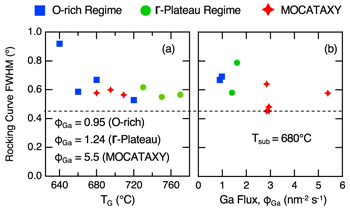
Fig. 3. (Color online) (a) and (b) FWHM (i.e. Δω values) are plotted as a function of TG and ϕGa , respectively. Values are obtained by transverse XRD scans of the  peak of α-Ga2O3 grown films (XRD data not shown). Three distinct growth regimes are studied in panels (a) and (b): (i) the O-rich rich regime (blue squares), (ii) the Γ-plateau regime (green circles), and (iii) the MOCATAXY regime (red stars). The lowest value of Δω is indicated by a dashed line. Note that for the samples grown by MOCATAXY, ϕIn was varied between (2.6–2.8) nm−2 s−1 and might explain the slight variations observed in Δω for α-Ga2O3 grown at ϕGa = 2.9 nm−2 s−1 in panel (b)].
Download figure:
Standard image High-resolution imageFinally, to directly quantify and identify how MOCATAXY affects the crystal structure of α-Ga2O3 thin films, high-angle annular dark-field STEM (HAADF-STEM) was performed along the  zone axis, and is plotted in Fig. 4. The sample shown here is the same as the one shown in Fig. 2(c). In Fig. 4(a), a clear contrast differentiates the sapphire substrate, the epitaxial film (α-Ga2O3), and the protective Au–Pd sputtered coating. The bright contrast observed at the substrate/film interface (see Fig. 4(b) and Ref. 27) is due to additional scattering of the electron beam and indicates the presence of misfit dislocations. These dislocations arise due to the film relaxation caused by strain. A subset of the observed misfit dislocations propagate and lead to threading dislocations. From the contrast variation observed within the film [see Fig. 4(a)], an average frequency of one threading dislocation every 30 nm laterally along the film/substrate interface is observed. While more investigation is needed to determine the cause of the faceting and verify the above hypothesis (e.g. due to the changed growth mode when using In-mediated catalysis), it is observed that the threading dislocations can merge and then continue to propagate toward the film surface. These dislocations terminate at the bottom of intersecting surface planes, where faceting along the (
 ) plane is observed. The complimentary facet is unidentified since the facet is not perpendicular to the beam and tilts out-of-plane. This tilting is detected in Fig. 4(a) by the fading of contrast along the surface, in contrast to the sharp change in contrast on the (
 ) plane.

Fig. 4. (Color online) HAADF-STEM images show an overview of an α-Ga2O3( ) film grown on α-Al2O3(
 ). (a) The epitaxial film shows increased contrast due to misfit dislocations at the film/substrate interface. Threading dislocation propagate through the film and terminating at the intersection of its surface periodic faceting. (b) Enlarged image of the film-substrate interface (i.e. the α-Al2O3–α-Ga2O3 interface) is shown. Burger circuits are drawn around the edge dislocations. (c) Fast Fourier transform (FFT) of the interface region is shown. Diffraction peak separation at (
 ) and (
 ) indicate strain relaxation of the α-Ga2O3(
 ) on α-Al2O3(
 ).
).
Download figure:
Standard image High-resolution image
Figure 4(b) shows an enlarged image of the film/substrate interface. A pair of edge dislocations is observed and is highlighted with their Burgers circuits. This edge dislocation pair is observed along the film/substrate interface, and its dislocation density is estimated to be 5 × 105 cm−1 (or ∼1011 cm−2), i.e. occurring every 20 nm. This is similar to what is reported by conventional MBE. 5) To quantify Al/Ga inter-diffusion at the interface, a line scan (see S-Fig. 2 Ref. 27) was performed to quantify the contrast change. An interface width of σ ≈ 0.9 nm was measured from an error function fitted to the Al intensity line scan profile (see S-Fig. 2 Ref. 27).
A fast Fourier transform (FFT), of the interface region shown in Fig. 4(b), is displayed in Fig. 4(c). A thin film completely strained to the substrate will show a singular diffraction peak. However, when the film relaxes its interplanar spacing dhkl changes, resulting in an additional peak, shifted from the substrate peak. However, shifted peaks in the in-plane direction are not visible because the α-Ga2O3 ( ) reflection peak is approximately 10x weaker than in α-Al2O3. The strain relaxation is observed in the
  and
and  diffraction peaks of α-Ga2O3. The strain relaxation is accomplished by the formation of edge dislocations at the interface, where the
  peak is correlated to the yellow Burgers circuit and the
  peak to the cyan Burgers circuit. In addition, no phase separation or secondary phases were observed by STEM within the α-Ga2O3 film grown by MOCATAXY. However, a bi-layer structure from overlapping α-Ga2O3 grains when viewed in projection is observed with a slip along the
 ![$[10\bar{2}\bar{2}]$](https://content.cld.iop.org/journals/1347-4065/62/SF/SF1013/revision5/jjapacbe04ieqn37.gif) direction (see S-Fig. 3 Ref. 27). The presence of this bi-layer structure indicates that the film is not single-crystalline. The bi-layer structure was confirmed using an ab initio TEM (abTEM) simulation
33) which produced a matching HAADF image from the crystallographic information framework.
direction (see S-Fig. 3 Ref. 27). The presence of this bi-layer structure indicates that the film is not single-crystalline. The bi-layer structure was confirmed using an ab initio TEM (abTEM) simulation
33) which produced a matching HAADF image from the crystallographic information framework.
This TEM investigation of MOCATAXY grown α-Ga2O3 shows comparable crystal quality to what is measured for conventional MBE 5) with regards to edge dislocation density and phase purity. We note that the difference in projection direction may have prevented imaging of the bi-layer structure in this previous report. No faceting of α-Ga2O3 was observed by conventional MBE when grown on m-plane α-Al2O3. 5,9)
4. Conclusion
Phase-pure α-Ga2O3( ) on α-Al2O3(
 ) was grown using conventional MBE and MOCATAXY with thickness up to d = 262 nm. We mapped out the Γ-dependence on ϕGa and TG and its impact on the crystalline quality and surface morphologies. We identified and explored previously inaccessible growth regimes by MOCATAXY, and showed that it vastly extends the growth regime and improves the out-of-plane mosaic spread of the grown α-Ga2O3 films. Using In-mediated catalysis, we observe facetting on top of the α-Ga2O3(
 ) layers. This study confirms that this new MBE growth mode can be applied to the growth of α-Ga2O3–and is not limited to the growth of the β-Ga2O3 and β-(Al,Ga)2O3 polymorphs. We emphasize more studies are needed to determine the kinetic parameters that form α-Ga2O3 during conventional MBE and MOCATAXY growth, as well as to further improve the quality of the grown α-Ga2O3/α-Al2O3 heterostructures, and to understand the mechanisms leading to the surface faceting of α-Ga2O3.
Acknowledgments
This research is supported by the Air Force Research Laboratory-Cornell Center for Epitaxial Solutions (ACCESS), monitored by Dr. Ali Sayir (FA9550-18-1-0529). J. P. M. acknowledges the support of a National Science Foundation Graduate Research Fellowship under Grant No. DGE2139899. M. A.-O. acknowledges financial support from the Central Research Development Fund (CRDF) of the University of Bremen. This work makes use of PARADIM under Cooperative Agreement No. DMR-2039380. This work uses the CCMR and CESI Shared Facilities partly sponsored by the NSF MRSEC program (DMR-1719875) and MRI DMR-1338010, and the Kavli Institute at Cornell (KIC).
Supplementary data (0.1 MB PDF)