

Abstract
Organic–inorganic lead halide perovskite materials have attractive properties not only for solar cells but also for LED because of their high performance and wavelength tunability. Such an efficient light-emitting and lasing nature are indispensable for their applications, and the essential needs are miniaturization and low lasing threshold. One material that satisfies these requirements is lead halide perovskite. To understand the time evolution of the interaction between light and matter in a perovskite crystal system, it is necessary to reveal the carrier dynamics in each crystal. In this study, the transient absorption spectra of CH3NH3PbBr3 crystals were measured using a femtosecond transient absorption microscopy. Surprisingly, strong spectra modulation has been observed and these results indicate the charge separation on the surface of the crystal. Amplified spontaneous emission dynamics were also observed in the transient absorption spectra.
Export citation and abstract BibTeX RIS
1. Introduction
Organic–inorganic lead halide perovskite materials have various attractive properties not only for solar cell 1–5) but also for LED and nanoscale lasers because of their wavelength tunability and low lasing threshold. 6–10) Such an efficient lasing is indispensable for their applications, and the essential needs are miniaturization and low threshold. One material that satisfies these requirements is lead halide perovskite (CH3NH3PbX3, X = Cl, Br, I). While this material was reported in 2009 for use in solar cells, it is also expected to be used in light-emitting and laser devices due to its easy tunability of emission wavelength and low-cost fabrication. However, the low-threshold lasing mechanism of lead halide perovskites has not been established due to various theories 11–14) on the interaction state between light and carriers generated in the cavity at the initial stage and the carrier–carrier interaction state, which has greatly hindered progress in improving performance. 15–18)
In terms of carrier dynamics in lead halide perovskite material, 19) Kamat and coworkers have reported the excitation intensity dependence of carrier dynamics and the carrier–carrier interaction. 20) Zhu and coworkers have reported the formation of the polaron in the initial stage preceding carrier generation and their recombination dynamics. 21) These reports were based on ensemble measurements in a film. On the other hand, the knowledge of the light and matter interaction based on the carrier dynamics in the single crystal level is also important to provide significant insights, because the dynamics of these carrier and light interactions can be hidden in the ensemble. 22–26)
In the present study, we have measured transient absorption spectra of a single CH3NH3PbBr3 microcrystal using a femtosecond transient absorption microscopy to reveal the initial carrier process that induces nonlinear luminescence.
2. Experimental methods
2.1. Sample preparation
CH3NH3PbBr3 crystals were prepared by a previously reported method. 8) Aqueous lead(II) acetate solution (100 mg ml−1) was dropped onto a glass slide and dried at 60 °C for 30 min to obtain a film of lead acetate. Microcrystals of CH3NH3PbBr3 were then obtained by immersing the film in methylammonium bromide solution (5 mg ml−1) with isopropanol as a solvent for 20 h at room temperature in air.
2.2. Transient absorption microscopy set-up
Transient absorption microscopy set-up was used in previously reported apparatus. 27–29) For transient absorption measurements, a regenerative amplified femtosecond pulse (Spectra-Physics, Solstice, 795 nm, 1 kHz) was split in two; the second harmonic of one beam was used as the excitation light, and the white light generated with the other beam by introducing it into an optical parametric amplifier (Light Conversion, TOPAS) and focusing the obtained signal light (1.3 μm) into a CaF2 plate was used as the probe light.
2.3. Calculation of the electronic spectra
The thin-film interferometry calculations were done using Eq. (1) which expresses general transmittance (T) light interferometry

where n, n 0 , and nm are the refractive index of the sample, air, and glass. b1 , b2 , b3 , and b4 are the amplitude parameters. γ and δ are the phase parameters.
The Franz–Keldysh calculation was done using the Eq. (2)

where R and ΔR are reflectances and ΔF represents a transient electronic field and A(F) is the combination of Airy functions.
3. Results and discussion
3.1. Results
Figure 1(a) shows the emission image of lead halide perovskite crystal excited with a femtosecond laser at 400 nm. Excitation intensity was 4.2 μJ cm−2. The pump light was sufficiently broader than the crystal to excite the whole crystal. Emission was observed over the crystal. Figure 1(b) shows the emission image of the same crystal excited at 11.4 μJ cm−2. Strong emissions were observed at both ends of the crystal. These results suggested that amplified spontaneous emission (ASE) or lasing occurred in the crystal, and as a result, these strong emissions have been observed to leak from the crystal edges.

Fig. 1. Emission image of lead halide perovskite excited with a femtosecond laser pulse at 400 nm. Excitation light intensities were (a) 4.2 μJ cm−2 and (b) 11.4 μJ cm−2.
Download figure:
Standard image High-resolution imageTo see the carrier dynamics in the crystal, the transient absorption microscopic technique was utilized. Figure 2(a) shows the transient absorption spectra in a lead halide perovskite excited at the intensities below the lasing threshold. The spectral signal was not observed before the time origin (−1 ps). The modulated spectral shape was significantly observed after the time origin (≥0 fs). The spectral bleaching around 540 nm indicates carrier generation by the excitation light, and the relaxation of the bleaching indicates the recombination of electrons and holes.

Fig. 2. (Color online) Femtosecond transient absorption spectra of a CH3NH3PbBr3 microcrystal excited with a femtosecond laser pulse at 400 nm. Excitation light intensities were (a) 4.2 μJ cm−2 and (b) 11.4 μJ cm−2.
Download figure:
Standard image High-resolution imageFigure 2(b) shows the transient absorption spectra in a lead halide perovskite excited at the intensities over the lasing threshold. A negative signal appeared around 557 nm, which was not present in the transient absorption spectrum excited at the intensity below the lasing threshold.
The differences in the spectra appearing with the excitation light intensity suggest the generation of stimulated emission signals. In fact, a strong luminescence signal is also observed in the emission image observations as shown in Fig. 1(b) under the condition over the threshold, supporting the idea that the appearing new band in Fig. 2(b) is due to ASE or lasing.
To reveal the different dynamics of ASE or lasing, Fig. 3 shows time profiles of transient absorbance monitored at 557 nm. When the excitation intensity was 11.4 μJ cm−2, in contrast to the result at the excitation intensity of 4.2 μJ cm−2, a notable decay with a time constant of 2 ps was observed. These results suggest the ASE or lasing process progressing in 2 ps. The time constant of ASE or lasing is consistent with previous reports. 11)

Fig. 3. (Color online) Time profiles of transient absorbance of CH3NH3PbBr3 microcrystals (Mon.540 nm).
Download figure:
Standard image High-resolution image3.2. Discussion
Spectral modulation is often observed as interference of light propagating in thin-film systems. The thickness of the perovskite crystals is around 200–300 nm, which is suitable to observe the optical interference. However, generally, this interference tends to become lower in frequency as one observes longer wavelengths, which is essentially different from the modulation observed here.
To discuss the optical interference effect, the actual optical interference pattern was simulated by using Eq. (1).
Figure 4 shows the calculation results by the thin-film interference model. The least mean-square fitting result was quite different from the experimental result. We tried several model calculations, including induced Raman signals and splitting signals with exciton-polaritons, but none showed good agreement with our results. If the modulation occurs during the time when light and matter are interacting with stimulated emission, the signal should disappear at 2 ps as shown in Fig. 3.

Fig. 4. (Color online) Calculated thin-film interference (solid red line) and transient absorption spectra at 1 ps after excitation (solid dotted line, 11.4 μJ cm−2).
Download figure:
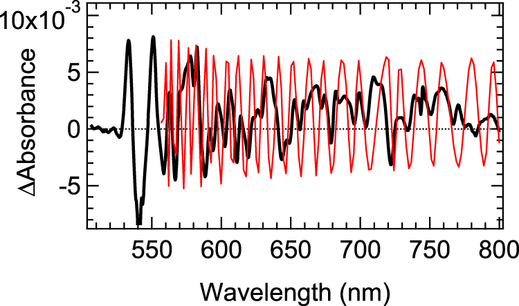
Standard image High-resolution imageThe spectra modulation appeared immediately after the carrier is generated, and the modulation continues for up to 1 ns. These results suggest that the modulation is caused by the electric field effect of the generated carriers on the electron spectrum. Franz–Keldysh theory is often used for spectral modulation in the presence of an electric field. In reflectance transient absorption spectroscopy, the electric field modulated spectrum has been explained in the GaInP2 system by the Franz–Keldysh theory in systems where charges are generated on the semiconductor surfaces. 30) The Franz–Keldysh theory could express this spectral modulation in high-frequency regions as shown in Fig. 5. These results indicate the spectral modulation mainly occurred from the charges trapping on the surface of the crystal. However, because of the complicated spectra shift and modulation, it is difficult to explain quantitatively how much electric field is generated. These results suggest that our transient absorption microscope measures the internal carrier dynamics differently from the surface by averaging the surface and internal charges, respectively. Transient absorption imaging measurements will clarify these differences in carrier dynamics between the edge and internal carrier, and we will report on unraveling ASE and lasing from the viewpoint of light–matter interactions in near the future. This technique will be also available for detecting charge accumulation to suppress lasing threshold for small laser media and provide design guidelines for more efficient and miniaturized lasing materials.

Fig. 5. (Color online) Calculated Franz–Keldysh interference (solid red line) and transient absorption spectra at 1 ps after excitation (solid dotted line, 11.4 μJ cm−2).
Download figure:
Standard image High-resolution image
4. Conclusions
The transient absorption spectra of CH3NH3PbBr3 crystals were measured using a femtosecond transient absorption microscopy. Strong spectra modulation has been observed and these results indicate the charge separation on the surface of the crystal. Amplified spontaneous emission or lasing dynamics was also observed in the transient absorption spectra.
Acknowledgments
This study was partly supported by KAKENHI Grant Numbers JP22H04755, JP19K05190, JST FOREST, and Tokushima University – Technion – Nichia Corporation collaboration (Tokushima International Science Institute (TISI)).