
Abstract
Molecular doping of organic semiconductors has been widely utilized to modulate the charge transport characteristics and charge carrier concentration of active materials for organic electronics such as organic photovoltaics, organic light-emitting diodes, and organic field-effect transistors. For the application of molecular doping to organic electronics, the fundamentals of molecular doping should be thoroughly understood in terms of doping mechanism, host and dopant materials, doping methodologies, and post-doping properties such as doping-induced structural/energetic disorder and doping stability. In this report, the fundamental understanding of molecular doping, types of dopants, doping methods, and their practical applications as organic field-effect transistors, organic photovoltaics, and organic thermoelectric are reviewed. Finally, key strategies for efficient molecular doping may exceed the trade-off relation between device performance and structural disorder.
Export citation and abstract BibTeX RIS
1. Introduction
Doping is the process of generating free electrons or holes by injecting impurities into a host semiconductor, which has been investigated since the beginning of the field of organic electronics. 1) Implementation of highly conductive polymers with conductivity comparable to that of metals by doping organics semiconductors (OSCs) has been one of the landmark discoveries. 2–5) On the other hand, doping has been carried out to modulate the charge transport characteristics of various OSCs for organic electronics such as organic photovoltaics (OPVs), organic thermoelectrics (OTEs), organic light-emitting diodes (OLEDs), and organic field-effect transistors (OFETs). 6,7) However, unlike the well-established doping method of generating impurity states within the band gap through atomic substitution of heterovalent dopants in conventional inorganic semiconductors, the understanding of effective doping methods in OSCs has been relatively insufficient.
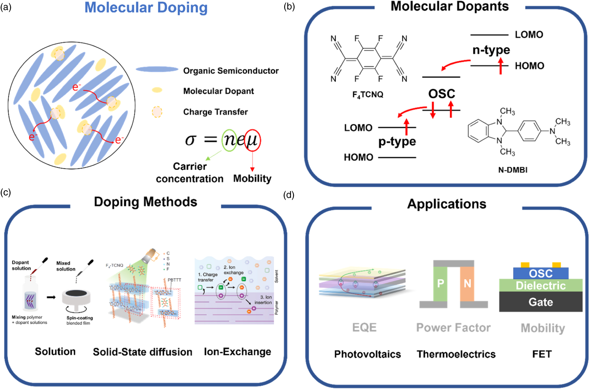
Molecular doping, employing external molecular dopants to induce charge transfer between dopants and host semiconductors, is one of the most promising methods for doping OSCs due to their structural and material compatibilities [Fig. 1(a)]. The research on molecular doping in OSCs has consequently been focused on understanding charge-transfer mechanism between dopants and OSCs, and the optimal molecular structure and electronic structure of dopants [Fig. 1(b)]. Another point-of-view is on the structural change upon molecular doping and the resulting change in the charge transport. Recent works on the doping methodology are dealing with this structural change and charge transport behavior to reduce the change in the molecular arrangement as the dopant molecule is incorporated in OSC [Fig. 1(c)]. A few reports on the development of the doping method showed effective molecular doping without severe structural change which reduces the mobility of the charge carrier. Such achievements will draw the doping of OSCs to a wider range of applications such as OPVs, OTEs, and OFETs for dramatic performance improvement as realized in the case of OLEDs [Fig. 1(d)]. 8) In this review, we will cover the fundamentals of the molecular doping mechanism of OSCs, the range of materials and processing methods for efficient doping, and comprehensively focus on doping concepts utilized in device applications such as OTEs and OFETs, for which OSCs show intrinsic material advantages to transform the future industries.

Fig. 1. (Color online) (a) Overview of molecular doping in organic semiconductors. (b) Schematic of energetics involved in molecular doping with representative p-type (F4-TCNQ) and n-type (N-DMBI) dopant molecules. (c) Representative doping methods in organics. Reproduced with permission. 9) Copyright 2016, Nature Publishing Group. And Ion-exchange doping method. Reproduced with permission. 10) Copyright 2021, Wiley. (d) Device applications of molecular doping and their device performance criteria.
Download figure:
Standard image High-resolution image2. Molecular doping
2.1. Mechanism of molecular doping in organic semiconductors
In the case of conventional inorganic semiconductors, doping is conducted by injecting dopant atoms that have different numbers of valence electrons compared with host atoms (B for p-type doping or P for n-type doping Si). When the incorporated dopant atoms are donor impurities (i.e. n-type doping), the dopant atoms generate donor states near the conduction band of the intrinsic semiconductor, and then extra free electrons can be generated in the conduction band by the excitation of electrons from the donor states. Conversely, free holes can be generated from the incorporation of acceptor impurities via the excitation of electrons from the valence band to the acceptor states formed near the valence band, creating holes in the valence band (i.e. p-type doping).
On the other hand, the doping of OSCs is carried out by molecular dopants rather than atomic dopants like in inorganic semiconductors. When host OSC and molecular dopant are put in proximity, charge transfer occurs driven by the energy level difference ( or
or  ) between the energy levels of the host OSC and those of the dopant molecule as shown in Fig. 2(a). The energy level difference between the dopant and OSC is a good indicator for predicting the charge transfer mechanism, i.e. whether the doping process of the OSC-dopant system occurs via ion pair formation [IP, Fig. 2(b)] or the formation of charge-transfer complexes [CTCs, Fig. 2(c)].
7) However, such indicator based on the energy differences requires careful attention since
) between the energy levels of the host OSC and those of the dopant molecule as shown in Fig. 2(a). The energy level difference between the dopant and OSC is a good indicator for predicting the charge transfer mechanism, i.e. whether the doping process of the OSC-dopant system occurs via ion pair formation [IP, Fig. 2(b)] or the formation of charge-transfer complexes [CTCs, Fig. 2(c)].
7) However, such indicator based on the energy differences requires careful attention since 

 and
and  are obtained from the isolated single molecules, not reflecting accurate conditions that charge transfer occurs (i.e. solid-state). Therefore, more sophisticated modelling of charge transfer mechanism should be established.

Fig. 2. (Color online) (a) Energetics rule for different charge-transfer doping mechanisms (IP and CTC) according to  and
and  (b) Ion Pair Formation (IP) mechanism. (c) Charge-transfer complexes (CTC) mechanism. (d) Energy level, and different degrees of charge transfer
  of P3HT/F4TCNQ and 4 T/F4TCNQ. Adapted from Ref. 12. Published 2015 by the Nature Publishing Group. (e) Integer Charge Transfer Complex (ICTC) mechanism. Reproduced with permission.
17) Copyright 2018, Nature Publishing Group.
of P3HT/F4TCNQ and 4 T/F4TCNQ. Adapted from Ref. 12. Published 2015 by the Nature Publishing Group. (e) Integer Charge Transfer Complex (ICTC) mechanism. Reproduced with permission.
17) Copyright 2018, Nature Publishing Group.
Download figure:
Standard image High-resolution image2.2. Ion pair formation
In principle, the LUMO level of p-type molecular dopants should be deeper than the HOMO level of OSC to generate free holes (i.e.  ), while the n-type molecular dopant should have a HOMO level shallower than the LUMO of the OSC to generate electrons in the OSC (i.e.
  ). In the IP mechanism, a whole integer of charge is transferred between a molecular dopant and the host OSC, which ionizes the dopant during doping and generates a
  charge in OSC, thus forming an ion pair [Fig. 2(b)].
11) Energetics related to Coulomb interaction between the molecular dopant and the OSC can be considered in describing the charge transfer process by the ion pair energy, E, between the dopant and the OSC in the following form
8)
charge in OSC, thus forming an ion pair [Fig. 2(b)].
11) Energetics related to Coulomb interaction between the molecular dopant and the OSC can be considered in describing the charge transfer process by the ion pair energy, E, between the dopant and the OSC in the following form
8)

where δ is the degree of charge transfer, k is the Coulomb constant, e is the electric charge, r is the distance between the electron and the hole, IE is the ionization energy, and EA is the electron affinity. Herein, Eq. (1) reveals that δ determines the ion pair energy, and the amount of charge transferred through this OSC−dopant interaction is determined at the value of δ that minimizes E. The degree of charge transfer can be quantified through Fourier-transform infrared spectroscopy (FTIR) [Fig. 2(d)].
12) Méndez et al. reported that the degree of charge transfer linearly scale with the observed frequency shift ( ) in FTIR as the following
13)
) in FTIR as the following
13)

where  and
and  denote the vibrational frequencies of the neutral dopant and that of its radical anion, respectively.
The above two models have been shown to accurately predict doping efficiency via IP formation, and therefore the resulting carrier mobility and electrical conductivity of the doped OSC. 8) Furthermore, considering the ion pair energy above, the optimal dopant can be selected for the target host OSC. The accuracy of this prediction can be further improved by measuring the exact EA and IE values of the dopant and host OSC at the corresponding doping levels and doping conditions (i.e. in solid-state) since the EA and IE values used for the calculation are often the values theoretically calculated for those of isolated molecules in vacuum state.
2.3. Charge-transfer complexes (CTC)
Unlike the IP mechanism, if the number of electrons transferred to OSC per dopant molecule is less than  the doping between the molecular dopant and the OSC occurs through the formation of CTC rather than IP. In the CTC mechanism, the frontier orbitals of the host OSC and molecular dopant are hybridized to form new sets of hybrid orbitals [Fig. 2(c)].
14) The degree of hybridization and the resulting energy splitting of the molecular orbitals depend on the energetics and spatial extent of each orbital. When CTC is formed, free charges are not immediately generated like in the case of IP. Charge transfer proceeds through the hybridized orbital, therefore the amount of charge transfer is limited owing to the higher energy level of the empty hybrid state (several tenths of eV) compared with HOMO of OSC (for p-type doping). This partial charge transfer leads to low doping efficiency and generally low conductivity compared to the OSCs doped by IP formation.
12,15)
the doping between the molecular dopant and the OSC occurs through the formation of CTC rather than IP. In the CTC mechanism, the frontier orbitals of the host OSC and molecular dopant are hybridized to form new sets of hybrid orbitals [Fig. 2(c)].
14) The degree of hybridization and the resulting energy splitting of the molecular orbitals depend on the energetics and spatial extent of each orbital. When CTC is formed, free charges are not immediately generated like in the case of IP. Charge transfer proceeds through the hybridized orbital, therefore the amount of charge transfer is limited owing to the higher energy level of the empty hybrid state (several tenths of eV) compared with HOMO of OSC (for p-type doping). This partial charge transfer leads to low doping efficiency and generally low conductivity compared to the OSCs doped by IP formation.
12,15)
However, it is yet unclear exactly which physical properties of OSCs and dopants lead to doping by IP or CTC, other than the simple energetic considerations outlined above.
16,17) For instance, in the case of integer charge transfer complex (ICTC) [Fig. 2(e)], it is in the form of ion pairs, however as in the case of CTCs, additional energy is required to overcome the binding energy required to generate a free charge.
16,17) Tietze et al. proposed that integer-charge-transfer doping is a two-step process (rather than a single step), which involves firstly a single-electron transfer from donor to acceptor molecule forming a ground-state ICTC and secondly the dissociation of the ground-state ICTC via thermal activation to free (i.e. separated) charges [see Fig. 2(e)].
17) The doping efficiency is directly linked to the dissociation of ICTCs, which demonstrates that selection criteria for optimal doping are not only related to synthesizing host-dopant molecules with the energetic requirements of  but also optimizing considerable factors such as interface energetics regarding electrostatics and degree of energetic disorder related to dissociation of IPs.
17)
but also optimizing considerable factors such as interface energetics regarding electrostatics and degree of energetic disorder related to dissociation of IPs.
17)
2.4. Types of molecular dopants
The molecular dopant is a neutral small molecule that can transfer a charge through a thermodynamically reversible reaction without breaking the covalent bond of OSCs. In the case of a p-type molecular dopant, an electron in the HOMO of the OSC is transferred to the LUMO of the dopant, and in the case of an n-type molecular dopant, an electron in the HOMO of the dopant is transferred to the LUMO of the OSC [Fig. 2(a)].
2.5. p-type molecular dopants
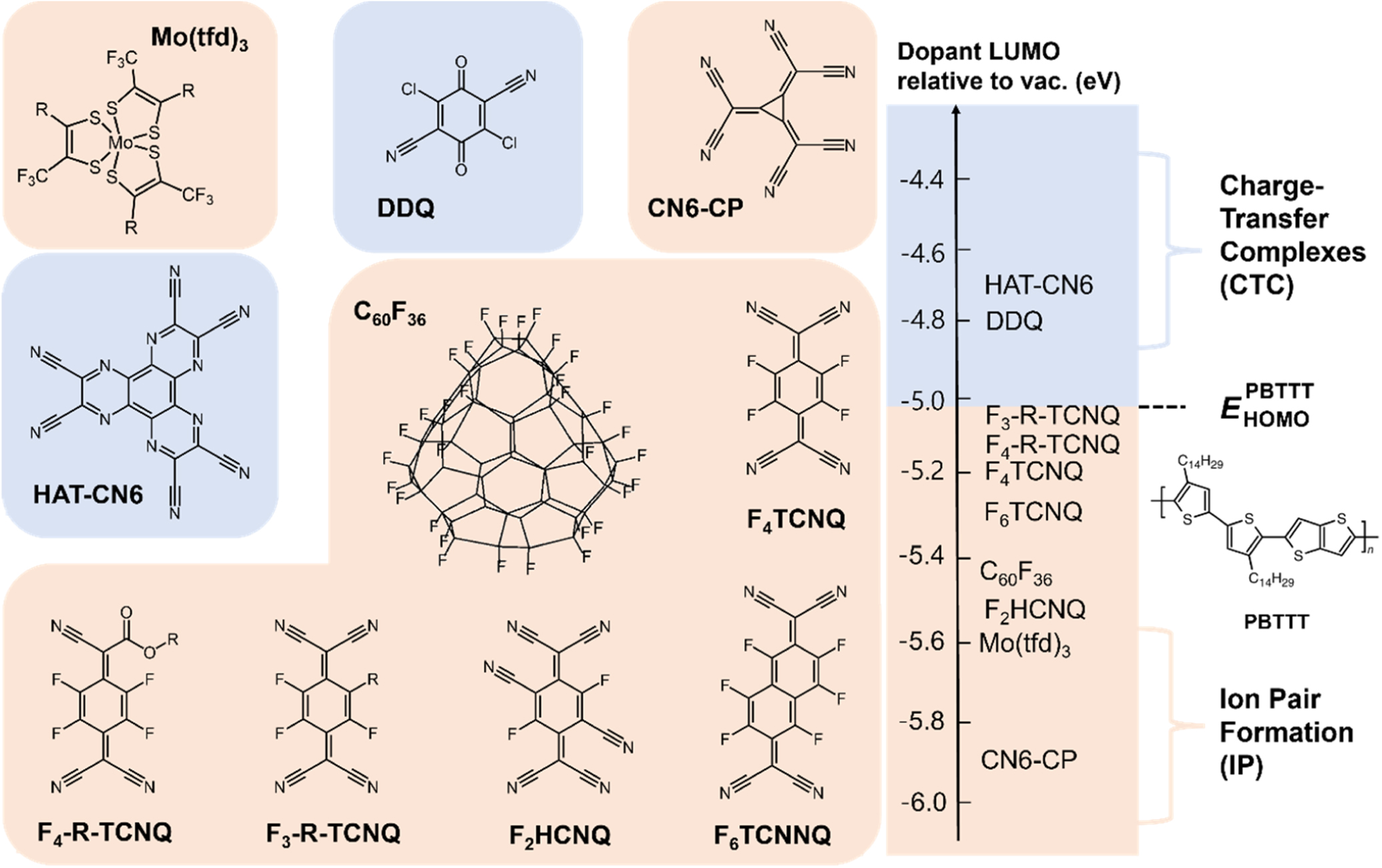
Initial studies on p-type molecular dopants were mostly related to the investigation of quinone molecules 18,19) (i.e. conjugated molecules derived from aromatic molecules with a cyclic dione structure), owing to the unsaturated aromatic ring structure. This structure increases the EA of p-type molecular dopants, facilitating the charge transfer process and improving the doping efficiency. Tetracyanoquinodimethane (TCNQ) is a representative example of p-type molecular dopants, however, the doping efficiency of TCNQ can be low due to a relatively low EA of TCNQ (LUMO ∼ −4.3 eV) compared to general HOMO levels of p-type OSCs. Méndez et al. studied the influence of fluorination on the aromatic core and showed that fluorination makes TCNQ electron-deficient, increasing the EA of TCNQ and doping efficiency. 20,21) Consequently, 2,3,5,6-Tetrafluoro-tetracyanoquinodimethane (F4TCNQ) prepared by replacing 2,3,5,6-hydrogens of the aromatic core with fluorine showed the highest increase in the EA by 0.9 eV, leading to a high doping efficiency. This molecular dopant is one of the most widely used p-type molecular dopants to date. 22) In addition, 3,5-difluoro-2,5,7,7,8,8-hexacyanoquinodimethane (F2HCNQ) was designed, which is a TCNQ molecule with 2,3,5,6-hydrogens replaced with two nitrogen and two fluorine atoms, with a further increase in the EA by 0.25 eV compared with F4TCNQ. 23) Another structural modification of TCNQ is introducing ester groups to control the solubility of the dopant. Among these F4TCNQ analogs, dopants with the diester group not only showed the adjusted solubility of the dopant but also stabilized the doping of poly(3-hexylthiophene) (P3HT) by dimerization reaction between diester groups which suppressed the diffusion of the dopants within the P3HT film. 24) Furthermore, new molecular structures were introduced for high electron affinities, such as 1,3,4,5,7,8-hexafluorotetracyanonaphthoquinodimethane (F6TCNNQ), 2,3-dichloro-5,6-dicyanobenzoquinone (DDQ), Dipyrazino[2,3-f:2',3'-h]quinoxaline-2,3,6,7,10,11-hexacarbonitrile (HAT-CN6), and hexacyano-trimethylene-cyclopropane (CN6-CP), with a planar molecular structure and C60F36, C60F48, molybdenum tris(1,2-bis(trifluoromethyl)ethane-1,2-dithiolene) (Mo(tfd)3) with a bulky, 3D structure.
According to the aforementioned doping mechanism, the possible doping mechanism of each molecular dopant can be predicted by calculating the ΔEp between OSC and dopant [Fig. 3]. For a representative p-type OSC, poly[2,5-bis(3-tetradecylthiophene-2-yl)thieno[3,2-b]thiophene] (PBTTT) with HOMO level of ∼ −5 eV, the dopants such as HAT-CN6 and DDQ are more likely to form CTCs, while dopants such as F3-R-TCNQ, F4-R-TCNQ, F4TCNQ, F6TCNQ, C60F36, F2HCNQ, Mo(tfd)3, and CN6-CP are more likely to form IP, although detailed energetic considerations should also involve the Coulomb interaction and the dissociation of the resulting IPs.
2.6. n-type molecular dopants
n-type molecular dopants usually have a shallower HOMO level (low IP) than the LUMO level of OSCs for efficient electron transfer from the HOMO of dopants to the LUMO of OSCs. Ironically, one of the biggest problems to be solved with n-type doping is that the chemical stability of dopants is low due to the shallow HOMO level, which means n-type dopants are readily oxidized. 25) Therefore, developing an n-type dopant is challenging due to the restrictions set by the LUMO of the OSCs, as well as the oxidation potential. Demand for n-type dopants for efficient and stable doping is increasing since the device applications such as OLEDs, 26–29) complementary circuits, 30–32) and thermoelectric generation all simultaneously require both p- and n-doping. 33–35) Even though various materials and methods were introduced for n-type doping of OSCs such as (i) using alkali metals, 36–38) (ii) molecular compounds with significantly shallow HOMO, 39–43) and (iii) air-stable precursor molecules that can donate an electron to the matrix material in the deposited film, 44–46) we focus here on the latter two due to the doping stability of alkali metals, 47)
One of the earliest works on n-type molecular dopants with low IE is bis(cyclopentadienyl)-cobalt(ΙΙ) (cobaltocene, CoCp2), which is a strong reducing agent with an ionization energy of about 4 eV, and an n-type dopant capable of shifting the Fermi level of OSC by 0.5 eV to the conduction band. 43) In addition, interfacial doping of CoCp2 reduced the charge injection barrier at the Au/PEDOT:PSS interface, demonstrating decent current enhancement that is comparable to that of p-doping of N,N'-diphenyl-N,N'-bis(1-naphthyl)−1,1'-bi-phenyl-4,4'diamine (α-NPD) with F4TCNQ. Hydride transfer doping is another way for efficient and stable n-doping of OSC because the Fermi level of OSC can be controlled by hydride doping and the main deciding factor for the selection of OSC for a given dopant is hydride affinity, instead of the electron affinity. (4-(1,3-dimethyl-2,3-dihydro-1H-benzimidazole-2-yl)phenyl)dimethylamine (N-DMBI) showed good controllability in the Fermi level of various n-type OSCs through hydride transfer doping. 39) In the case of FETs incorporating C60 or C70, bias-stress measurement results showed that the bias-stress stability is improved by N-DMBI doping compared to the other n-type OSCs owing to the filling of shallow electron traps in the pristine films. 39) Benzyl viologen (BV) and diquat (DQ) are commonly used n-type dopants and have recently been used for doping of bulk heterojunctions (BHJs) as a way to improve the performance of OPVs by improving the film morphology and suppressing the trap density. 40,41)
According to the aforementioned doping mechanism as in p-type dopant, a similar approach can be taken to predict the possible doping mechanism of each molecular dopant with  For a representative n-type OSC, naphthalene diimide (NDI), which has LUMO of ∼−3.7 eV, dopants such as DQ, CoCP2, N-DMBI, zinc phthalocyanine (ZnPc) and tetrabutylammonium fluoride (TBAF) are more likely to form CTCs, while tetrakis(hexahydropyrimidinopyrimidine)ditungsten(II) (W2(hpp)4), BV and mesitylene pentamethylcyclopentadienyl ruthenium dimer ([RuCp*(mes)]2) are more likely to form IPs [Fig. 4].
2.7. Doping method
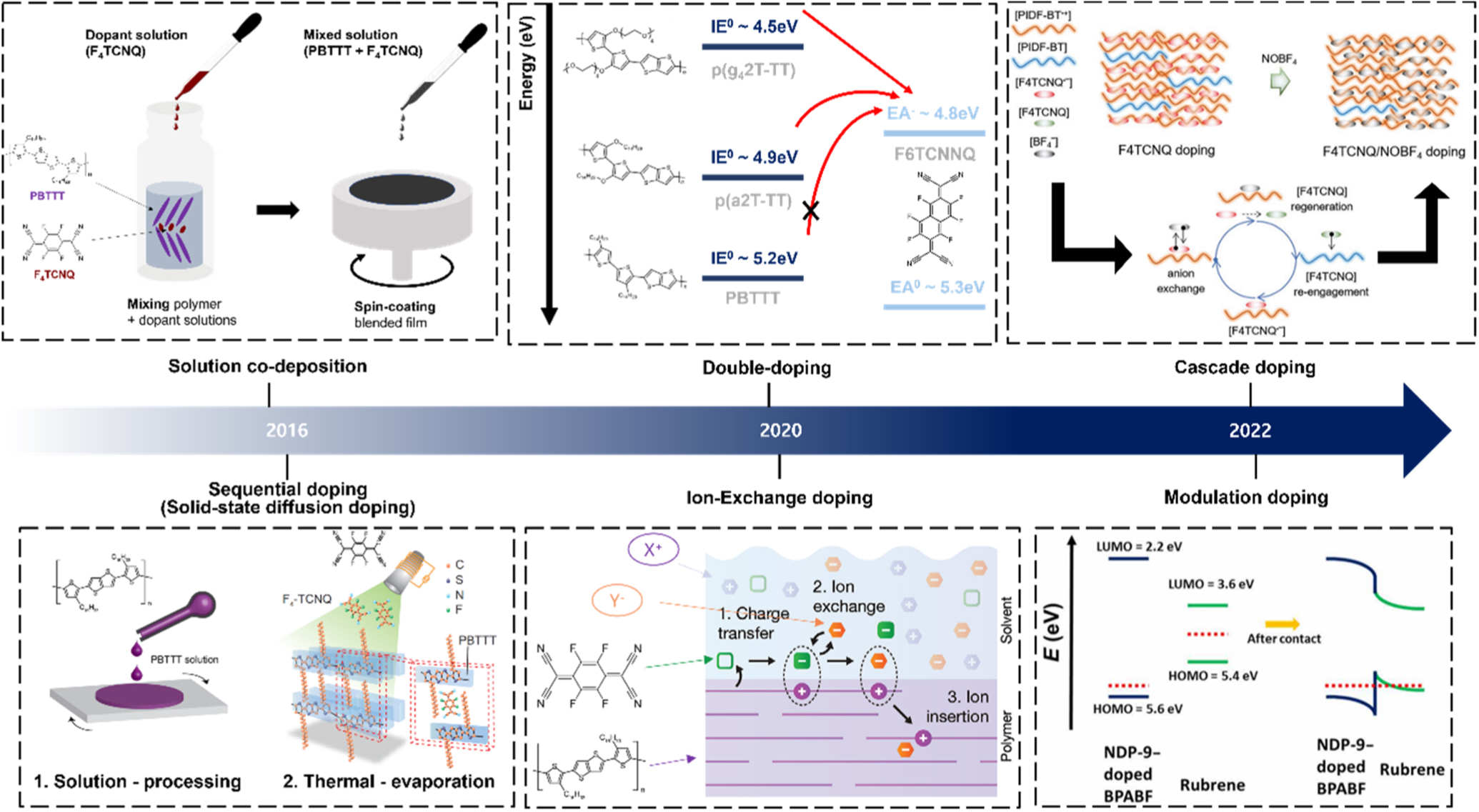
In this section, various implementation examples of doping will be introduced by addressing methodological differences and features based on the aforementioned materials and doping mechanisms [Fig. 5]. Doping methods can be divided into two major types: (i) co-deposition and (ii) sequential deposition. The sequential deposition methods can be further classified into four small categories: solid-state diffusion, ion-exchange, cascade, and modulation. Here, we outline the basic principles and main differences between the above doping methods in order to discuss their implications in device applications in detail in the next section.
2.8. Co-deposition method
Co-deposition method involves doping by dissolving dopants in the same solvent as that of the host semiconductor. Doped films can be deposited by spin coating or blade coating the blended solution with a desired ratio of OSC to dopant. The advantage of this method lies in the controllability of the doping ratio by simply mixing the desired ratio of OSC to dopant in the blended solution. 42) However, the solubility of dopant molecules can be limited in good solvents for the host OSCs, and the solubility of the OSC decreases as doping proceeds due to the ionization of the OSC. Therefore, the limited solubility of both the OSC and the dopant causes aggregation in the solution, leading to undesirable defects in the morphology of the cast, 48) which limits the electrical conductivity of the doped OSC.
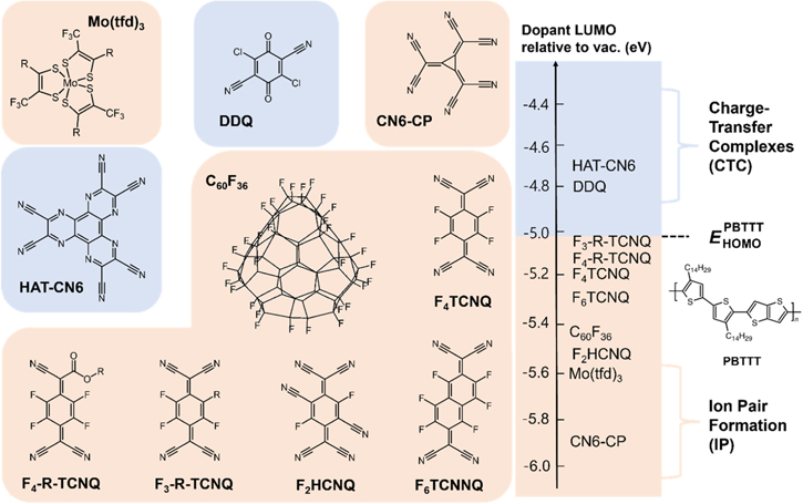
Fig. 3. (Color online) Representative p-type dopant molecules with their predicted charge transfer mechanism relative to PBTTT according to the energetics rule [see Fig. 2(a)].
Download figure:
Standard image High-resolution image2.9. Sequential deposition method
Unlike the co-deposition method, the sequential deposition method involves the deposition of dopants onto the pre-deposited OSC film. The deposited dopant molecules infiltrate into the OSC film and dope the OSC. Therefore, it is hard to estimate the doping efficiency because the infiltration of the dopant molecule may not be uniform over the whole OSC film. Therefore, additional analysis techniques such as UV–vis-NIR spectroscopy, photoluminescence quenching, and ultraviolet photoelectron spectroscopy (UPS) should be complemented to quantify how many dopant molecules have penetrated into the OSC film for calculating the doping efficiency. 49)
2.10. Solid-state diffusion method
The solid-state diffusion method is a sequential doping method that deposits the dopant molecules on OSC film by the evaporation of dopant molecules. The dopant molecules diffuse into the OSC film and dope OSC molecules in solid-state without employing any solvents during the doping process. Kang et al. studied the solid-state diffusion of F4TCNQ in highly crystallized PBTTT polymer thin film. 9) This study shows that the doping of PBTTT was effectively conducted by solid-state diffusion of F4TCNQ while maintaining the local crystalline π–π stacked structure of PBTTT that facilitated coherent charge transport properties similar to that of free electrons. The resulting doping concentration was maximised by bulk-incorporating dopant molecules in PBTTT film and the electrical conductivity that can be achieved with this doping method was more than 200 times (∼250 S cm−1) larger than that of the solution co-deposition method. 9)
2.11. Double-doping effect
Maximising doping ratio can be achieved not only by processing but selecting the right OSC-dopant combination. Ideally, doping ratio can be more effective if one could transfer more than one charge per dopant molecule since this could lead to lowering of the dissociation energy and enhancement of the doping efficiency. 50) Ionization efficiency could be enhanced by using a dimer dopant which transfers two charges per dopant molecule. However, ionized dimer dopants are split into two separate entities, instead, that act as counterions inducing structural disorder. 51–53) Kiefer et al. demonstrated double-doping using a common p-type dopant, F4TCNQ that could accept two electrons per dopant molecule from the host semiconductor even without dimerization. Double-doping occurs through a two-step process; (i) neutral dopant molecule which has the EA deeper than IE of the host semiconductor generates a hole in the host OSC and the neutral dopant is ionized. (ii) Even ionized dopant anion still has the EA deeper than the IE of the oxidized OSC, and therefore an additional hole can be transferred from the dopant anion to the host OSC. 50) By investigating different semiconductor−dopant combinations, the effect of dopant concentration, and doping efficiency, this study suggests that the double-doping effect is a generic principle that could lead to ionization efficiency of up to 200%.
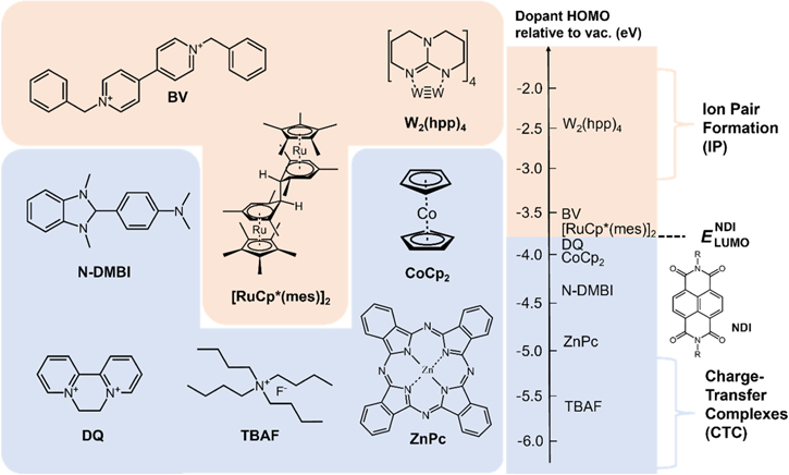
Fig. 4. (Color online) Representative n-type dopant molecules with their predicted charge transfer mechanism relative to NDI according to the energetics rule [see Fig. 2(a)].
Download figure:
Standard image High-resolution image
Fig. 5. (Color online) Timeline of doping method developments for conjugated polymers from conventional solution co-deposition method to sequential doping method (e.g. solid-state diffusion doping 9)), double-doping, 50) ion-exchange doping, 10,54) cascade doping 55) and modulation doping. 59) Reproduced with permission. 9) Copyright 2016, Nature Publishing Group. Double-doping method. Reproduced with permission. 50) Copyright 2019, Nature Publishing Group. Ion-Exchange method. 10,54) Reproduced with permission. 10) Copyright 2022, Wiley. Cascade doping method. Reproduced with permission. 55) Copyright 2020, Wiley. Modulation doping method. Reproduced with permission. 59) Copyright 2022 American Association for the Advancement of Science.
Download figure:
Standard image High-resolution image2.12. Ion-exchange doping method
The ion-exchange doping method is a two-step method consisting of a molecular doping process and an ion-exchange process. The first step is a general molecular doping process, which involves incorporation of dopants in the host semiconductor film for inducing charge transfer between the dopant and OSC. After that, the doped OSC film is brought in contact with an ionic liquid in which an ion-exchange occurs between the dopant ion in the OSC film and an ion in the ionic liquid. The above method was implemented in the form of p-type doping of PBTTT, and it was reported that the doping occurs through the replacement of F4TCNQ radical anion with a Y−anion of an ionic liquid (existing in X+Y− type) [Fig. 6]. 54) This eventually leads to the IP formation of a PBTTT radical cation and a Y−anion. The ion-exchange method has been found to be particularly effective for a certain combination of ionic liquid and OSCs, and the ion conversion rate was discovered to reach up to 100%. 10)

Fig. 6. (Color online) (a) Conductivity and (b) extracted mobility for C60 doped with [RuCp*(mes)]2 for three different temperatures. Reproduced with permission. 62) Copyright 2012, APS. (c)–(d) Experimental data (C–V measurement, I–V measurement) and numerical modeling data of F4TCNQ-doped P3HT films. Reproduced with permission. 11) Copyright 2013, APS. (e) Coulomb potential wells created by the ionized dopants at low and high doping ratios. Reproduced with permission. 67) Copyright 2005, APS.
Download figure:
Standard image High-resolution image2.13. Cascade doping method
The cascade method is a type of ion-exchange doping method improving the doping efficiency by mixing multiple dopant molecules. 55) In a recent study on cascade doping, F4TCNQ and NOBF4 were used as dopant molecules, in which neutral F4TCNQ molecules were found to be regenerated to engage in doping after anion-exchange occurred with NOBF4 − in PIDF-BF polymer, which led to improved doping efficiency with a high conductivity value exceeding 610 S cm−1.
2.14. Modulation doping method
The modulation doping method is widely used in inorganic semiconductors where a heavily doped wide bandgap semiconductor is brought in contact with a narrow bandgap semiconductor. 56–58) Generation of free charge carriers from the spatially separated dopants from the channel can minimize ionized impurity scattering, and therefore maximising the carrier mobility in the channel. 56–58) Wang et al. demonstrated an efficient modulation doping effect with a high-mobility crystalline OSC film, rubrene. 59) This study shows that high doping efficiencies (over 20%) can be reached through the modulation doping of vacuum-deposited rubrene thin-film crystals even for high dopant loadings.
2.15. Molecular doping in organic electronic devices
This section is relevant to relating molecular doping of OSCs for their applications in electronic devices and energy applications. In particular, doping effects in field effect transistors, thermoelectrics, and photovoltaics are addressed because the doping of active channel in these devices is critical to determining the device performance. In OFETs, doping can be applied to either the active channel region or the contact region to modulate the device characteristics and improve the carrier injection. For thermoelectrics and photovoltaics, tuning the charge carrier concentration is the key to maximising the power conversion efficiency (PCE) by improving the charge transport and charge extraction. All of the above benefits of doping can be better understood by discussing the effects on the charge transport of OSCs. In this section, the effect of doping in charge transport of OSCs is discussed first, then representative works of doping applications in OFETs and organic thermoelectrics in the hope of demonstrating the potential of doping strategies in organic electronics.
2.15.1. Doping effects in charge transport
Unlike inorganic semiconductors, the charge transport in OSC typically occurs via hopping of charge carriers owing to charges localized on trap sites originating from structural and energetic disorder within organic material. These trap sites act as energetic obstacles for charge carriers, leading to low charge carrier mobility. 60,61) Considering the transport nature of organic materials, charge transport in the undoped OSC can be improved by doping. Additional charge carriers released by the dopants lead to an increase in mobility by the filling of traps, reducing the number of trap sites to hop for charge carriers. 62) However, the charge carrier mobility of doped OSCs does not show a simple proportional increase with the doping concentration. In this section, we are going to elaborate on the doping effects on charge transport by discussing representative studies on the relationship between doping concentration and charge carrier mobility in OSCs and the two proposed mechanisms of mobility enhancement with increasing doping concentration.
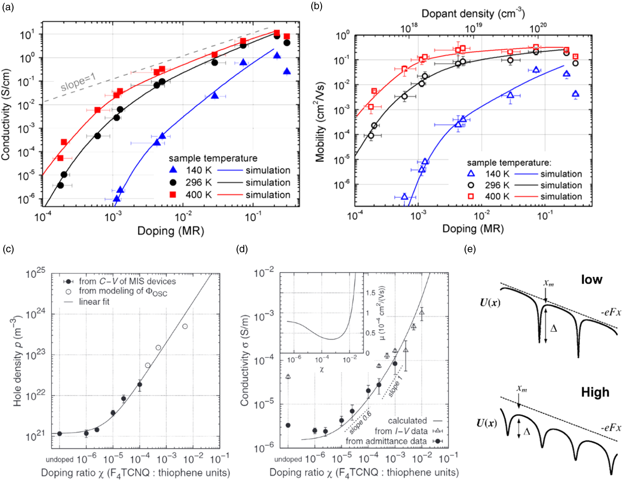
Olthof et al. demonstrated that trap filling leads to an increase in the charge carrier mobility through ultralow doping of C60 with ruthenium (pentamethylcyclopentadienyl) (1,3,5,-trimethyl benzene) dimer [RuCp*(mes)]2 [Figs. 6(a) and 6(b)]. 62) In the high-temperature regime, the measured electrical conductivity was shown to increase super-linearly with the doping concentration in the low doping regime, and almost linearly in the moderate-to-high doping regime. The transition (i.e. the slope change in conductivity versus doping concentration) occurs when most of the traps in OSCs are filled [Fig. 6(a)], with the slope being unity. In the low-temperature data set, the unity slope is not observed even at high doping concentrations since trap sites still play an important role. For the highest doping concentration (doping ratio of ∼0.3), the conductivity value starts to decrease owing to the large number of dopant molecules that can disrupt the molecular arrangement of the OSC film, presumably generating trap sites.
On the other hand, Pingel et al. established a rational description of the nonlinear behavior of conductivity with increasing doping concentration. 11) Using P3HT films doped by F4TCNQ, the authors found a sublinear increase in conductivity [Fig. 6(d)] at low to moderate doping levels (χ < 10−4), even though the hole density [Fig. 6(c)] at low doping level show a steeper increase, suggesting mobility decreases in this regime [Fig. 6(d), inset]. This can be attributed to the ionized F4TCNQ molecules which have a long range Coulomb interaction due to the low relative permittivity in OSCs, leading to a broadening of density-of-states (DOS) distribution [Fig. 6(e)]. The occurrence of Coulombic traps leads to a reduction of mobility at the low-to-moderate doping regime.
It is still on debate that which model is the best to describe the charge transport behavior of OSC with increasing doping level. Small molecule semiconductors showed that the trend in charge carrier mobility as a function of doping level is well-fitted with trap filling model (super-linear slope to linear slope), 17,63) while the trend in polymer semiconductors are well-fitted by the Coulomb scattering model (sublinear slope to linear slope). 64,65) This might be an interesting point suggesting that molecular structure affects the doping of OSC. Zen et al. reported that the molecular weight of polymer affects the charge transport of polymer semiconductors owing to the difference in the connectivity of crystal domains depending on the length of polymer chains. 66) Likewise, the difference in the connectivity of the crystal domain between small molecules and polymer semiconductors might be a key factor in this phenomenon. Due to the requirement of more direct evidence to systematically describe the charge transport behavior with a varying doping level of two different OSCs, further investigation using various electronic devices will be a good method for distinguishing the two models and understanding the effect of doping on the charge transport of OSC.
2.15.2. OFET
OFET has become an emerging device enabling electronic functionalities to be integrated on flexible, plastic substrates for a range of applications, including flexible electrophoretic displays, 68) radiofrequency identification (RFID) tags, 69) and organic light-emitting diode (OLED). However, FET mobility values are typically too low for practical applications (e.g. for high-performance RFID tags that operate at ∼MHz range). The low mobility values can be attributed to (1) low intrinsic mobility of OSC channel and (2) contact resistance originating from an injection barrier at the OSC-metal interface 70–72) which becomes dominant for short-channel devices. To mitigate these issues, there have been numerous attempts to employ molecular doping concepts for enhancing the channel mobility 73,74) and charge injection, 30,62,75) and also modulate the channel polarity for tuning the operation characteristics, 30,76) all of which will be elaborated in the current section.
2.15.3. Charge injection
The charge injection problem at the interface of OSC and metal electrode has been one of the critical obstacles that lower the performance of OFETs. 61) Contact doping (i.e. local doping of OSC near the contact region) can be an effective solution by either (1) reducing the energetic barrier for charge injection by bringing the Fermi level of OSC closer to the work function of the metal electrode, 77,78) or (2) narrowing the depletion layer formed at the Schottky barrier at the interface. However, contact doping could also interrupt molecular arrangement near the contact and increase trap density as a result, leading to poor charge injection. 79,80) Therefore, careful selection of dopants and doping method are required to improve the overall OFET performance.
As an example of effective contact doping, Kim et al. introduced "molecular implantation doping" method for extensively doping OSC selectively near the contact region, improving the charge injection of the bottom-gate bottom-contact PBTTT OFETs by solid-state diffusion of F4TCNQ [Fig. 7(a)]. 75) The OFETs fabricated using the contact doping technique showed a markedly improved charge injection from the contact resistance lowered by approximate factor of 5 [Fig. 7(e)]. The large energetic barrier [∼0.87 eV, Fig. 7(c)] at the metal/semiconductor interface is reduced after locally doping OSC near the contact due to the reduced depletion width induced by large doping concentration induced from the effective solid-state diffusion of F4TCNQ in PBTTT [Fig. 7(d)].
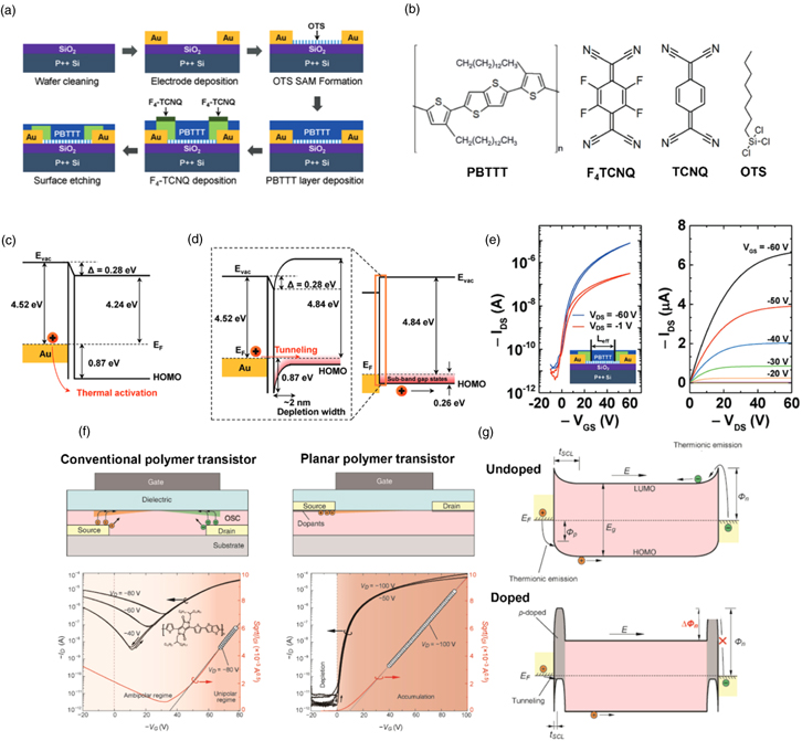
Fig. 7. (Color online) (a) Schematic images of the device fabrication process for contact doping via molecular-implantation doping for PBTTT OFETs. (b) Molecular structures of PBTTT, F4TCNQ, TCNQ, and OTS. (c) The band diagram at the Au/PBTTT interface for pristine PBTTT and (d) F4TCNQ-doped PBTTT. (e) IDS–VGS transfer curves and IDS–VDS output curves of contact-doped (doped/etched) PBTTT transistor. Reproduced with permission. 75) Copyright 2019, Wiley (f) Schematic and IDS–VGS transfer curves of conventional polymer OFETs with a staggered geometry and planar-processed polymer transistor, respectively (g) The band diagram of ambipolar charge accumulation for undoped (top) and contact-doped (below) polymer OFETs. Reproduced with permission. 76)Copyright 2016, Wiley.
Download figure:
Standard image High-resolution imageIn addition, molecular doping can be directly applied to the active channel of OFETs. For high-mobility donor–acceptor (D−A) copolymers, 81) their narrow HOMO-LUMO gap has been demonstrated as high-performance OFET channel material for ambipolar transport. However, only staggered device structures have been commonly utilized due to poor charge injection in planar structures [Fig. 7(f)]. Xu et al. demonstrated that reliable high-performance p-type OFETs could be made with a DA polymer, diketopyrrolopyrrole-thieno[3,2-b]thiophene (DPPT-TT), by employing contact doping in planar structure (top-gate top-contact). Contact doping with a p-type dopant, iron chloride (FeCl3), exhibited a lower contact resistance due to a simultaneous lowering of hole injection barrier and raising of an electron injection barrier [Fig. 7(g)]. Therefore, the enhanced hole injection and blocked electron injection led to a dramatic enhancement in hole mobility, showing ideal unipolar p-type FET transfer characteristics. 76)
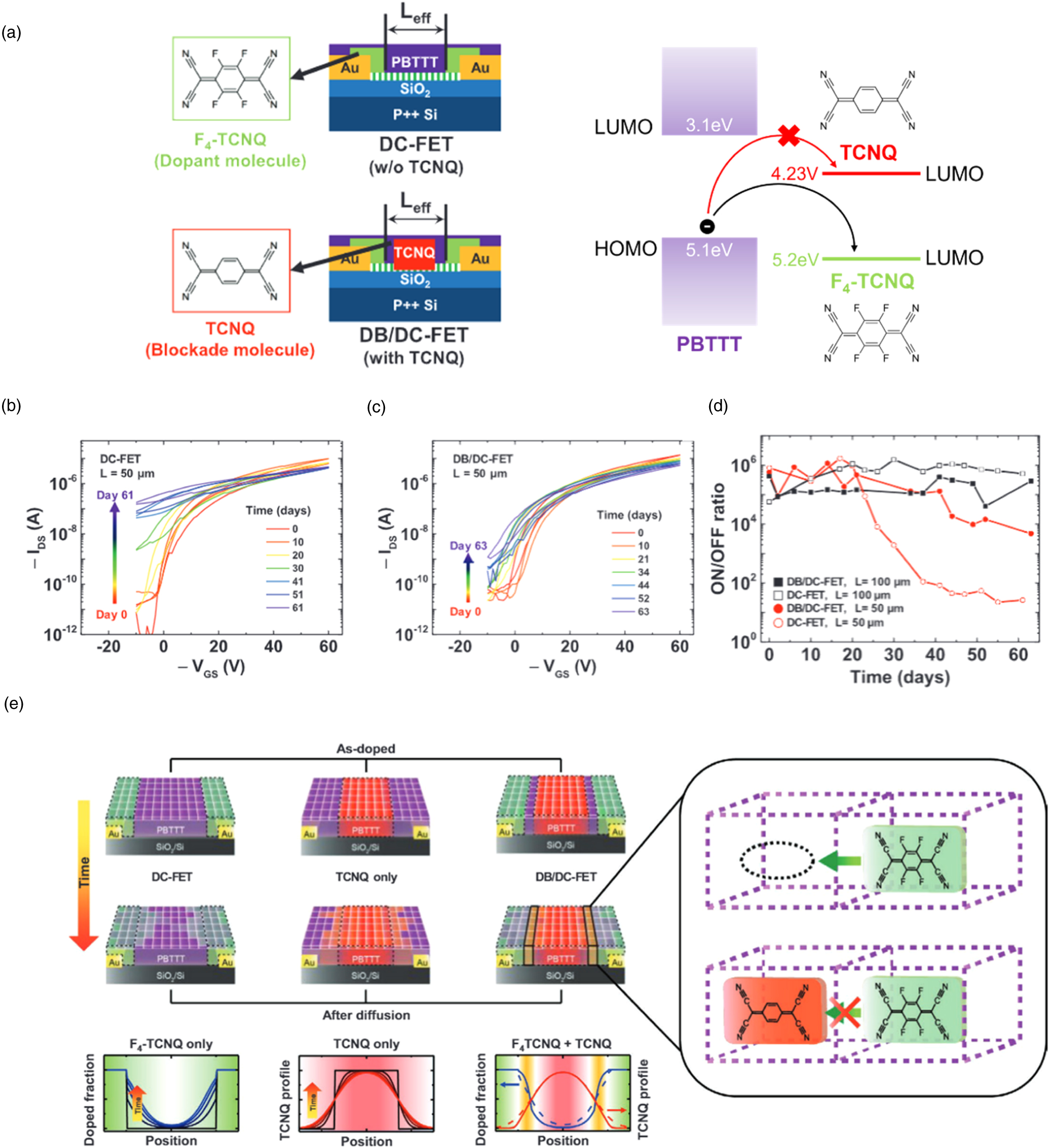
In the aforementioned contact doping works, however, the stability of contact doping was poor as the dopant molecules diffused toward the bulk of the channel. To overcome this problem, the dopant-blockade method was developed. 82) Kim and coworkers used F4TCNQ and TCNQ as a dopant and blockade molecule, respectively [Fig. 8(a)]. The blockade molecules were deposited in the middle of the OFET channel first, and then dopant molecules were deposited at the contact region. By comparing the stability of two devices with doped-contact stabilized by the dopant-blockade method (DB/DC) FET and without the blockade molecule deposition doped-contact (DC) FET, it is found that the doping stability reflected by the on/off ratio of the OFETs with the dopant blockade molecules was retained over 2 months, whereas that of DC-FET decreased significantly, which reflects an enhanced doping stability for with the proposed dopant-blockade method [Figs. 8(b)–8(d)]. The experimental results were also supported by numerical simulation of dopant diffusion in PBTTT channel and its suppression by site-occupying TCNQ molecules [Fig. 8(e)].
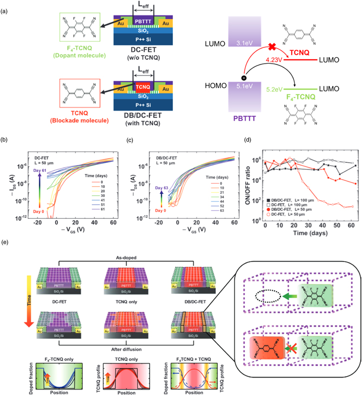
Fig. 8. (Color online) (a) The device schematics for FETs with doped-contact (DC-FET) and doped-contact stabilized by the dopant-blockade method (DB/DC-FET). (b)–(d) Their resulting transfer curves during the storage time over 2 months, respectively. (d) Device stability is reflected by the ON/OFF ratio stability of the DC and DB/DC-FETs. (e) The schematic representation of dopant diffusion in the PBTTT channel and its suppression by site-occupying TCNQ molecules (in the inset), as confirmed by numerical simulations. Reproduced with permission. 82) Copyright 2020, Wiley.
Download figure:
Standard image High-resolution imageOn the other hand, molecular doping has been shown not only effective in enhancing charge injection in OFETs but for improving charge extraction at the metal/OSC interface in OPVs. 41,83–85) Recently, Yan et al. improved PCE by more than 30% using the solid-state diffusion method, minimizing structural disorder even in the condition of relatively high doping concentrations. 43) This work demonstrated the feasibility of heavy doping in OPVs, enlarging the doping range applicable to OPVs. Another doping approach attempted has been focused on enhancing the charge transport within the BHJ of OPVs. 41) BV is incorporated in BHJ as an n-type dopant and synergistically improved the microstructure and reduced the trap density which led to increasing the power conversion efficiency from 13.2% to 14.4% upon the addition of the optimal concentration of 0.004 wt% of BV for inducing better molecular stacking.
2.15.4. Charge transport polarity modulation
Due to oxidative stability of the OSC channel, OSCs with high work function have been predominantly used for p-type FETs and most OSCs typically have higher hole mobility compared with electron mobility. However, for CMOS applications, both p- and n-type FETs are required, and therefore efficient hole and electron injection from the metal electrodes to the OSC channel, and retaining high on/off ratio values are demanded. Khim et al. doped initially ambipolar methanofullerene [6,6]-phenyl-C61-butyric acid methyl ester (PCBM) OFETs with an n-type dopant cesium fluoride (CsF) and a p-type dopant F4TCNQ, respectively by blending or inkjet printing of a dopant layer on the pre-deposited semiconductor film [Fig. 9(a)]. 30) Figures 9(b) and 9(c) show that 1.0 wt% doping ratio of CsF and F4-TCNQ drastically decrease the μFET,h, and μFET,e, respectively, suggesting three different operation regimes; (i) equivalent ambipolar transport with pristine PCBM, (ii) n-channel predominant operation with n-doped PCBM, and (iii) p-channel predominant operation with p-doped PCBM. Additionally, the turn-on voltage, Von, shift plot with p-doping and n-doping indicates an effective control of Von by appropriate doping level. Finally, the authors implemented a complementary ambipolar inverter with a selective molecular doping method using inkjet printing [Fig. 9(d)].
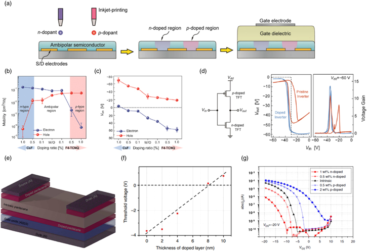
Fig. 9. (Color online) (a) Schematic representation of fabrication process (inkjet printing) of the complementary ambipolar inverter. (b) The electron and hole mobilities in of PCBM OFETs with different doping level. (c) Turn-on voltage (Von) of CsF-doped PCBM OFETs. (d) Circuit configuration of the complementary-like inverter and voltage transfer characteristics corresponding voltage gains of inverters based on two identical PCBM FETs (orange solid line), n- and p-doped PCBM FETs fabricated by inkjet-printed doping method (blue solid line). Ideal inverter curves (black dashed line) are displayed at Vdd = –60 V. Reproduced with permission. 30) Copyright 2014, Wiley. (e) Scheme of the transistors consisted with doped pentacene channel, intrinsic pentacene layer, and source and drain contacts prepared by the doping of pentacene. (f) The threshold voltage as a function of the thickness of doped layer. (g) The transfer characteristic of transistors using the same gate and contact electrode with varying doping concentration. Reproduced with permission. 87) Copyright 2013, Nature Publishing Group.
Download figure:
Standard image High-resolution imageAnother practical implementation of polarity modulation by molecular doping of OSC was the development of inversion-mode OFETs, which was hard to realize due to the inefficient injection of minority charge carriers into the inversion channel. 86) Lüssem et al. demonstrated both organic depletion and inversion transistors by setting up the transistors consisting of Al2O3 as a gate dielectric, a thin doped pentacene layer as the OFET channel, an intrinsic pentacene layer and doped source and drain contact electrodes [Fig. 9(e)]. 87) F6TCNNQ and W2(hpp)4 were used as a p-type dopant and an n-type dopant, respectively. The fabricated depletion-mode transistor showed a positive shift in the threshold voltage, Vth, according to appropriate doping conditions without sacrificing the on/off ratio, suggesting that the doped layer can be fully depleted with gate voltage. A linear shift of Vth with the thickness of the doped layer clearly supports generation of free charges into the channel [Fig. 9(f)]. As seen in Fig. 9(g), the n-doped transistors clearly show a p-type characteristic, and the threshold voltage increases with increasing n-doping concentration. This shift of threshold voltage is attributed to the formation of an inversion layer (i.e. the n-doped layer) at the oxide/pentacene interface, which is a clear demonstration of the inversion-mode transistor.
2.15.5. Thermoelectrics
A thermoelectric device capable of converting thermal energy into electrical energy is one of the most popular application fields of OSC doping. The figure of merit associated with the thermoelectric energy conversion, ZT, is represented by a combination of transport parameters

where σ is electrical conductivity, S is the Seebeck coefficient, k is thermal conductivity, and T is the absolute temperature. OSCs for thermoelectrics have been thoroughly studied due to their low thermal conductivity (in the order of 0.1 W mK−1), 88) which is advantageous for high ZT values. Additionally, organic materials hold promises for their mechanical flexibility, cost-effectiveness, and eco-friendly processing. 89) In terms of the commercialization of thermoelectric devices, it is known that there is practical significance when the value of ZT is higher than 1. There have been intensive efforts in improving the ZT value of organic thermoelectric devices which is generally lower than that of inorganic materials. 90) However, the above transport parameters are correlated to each other, and independent improvement of one parameter is not possible to realize. 91) For instance, increasing electrical conductivity accompanies an increase in thermal conductivity (Wiedemann–Franz law), however, the Seebeck coefficient is inversely proportional to the electrical conductivity, compromising the ZT value as a result [Fig. 10(a)]. Therefore, to optimize ZT to develop high-performance thermoelectric devices, it is essential to discern physical relationships and develop dopant and active materials 92) for increasing S, σ, and k simultaneously. 93–95) In particular, most organic thermoelectric material research has focused on increasing the value of the thermoelectric power factor, σS2, which is the maximum thermal energy conversion output of the material. 96)

Fig. 10. (Color online) (a) Trade-off between conductivity ( ) and Seebeck coefficient (S). (b)–(c) Comparison of the Seebeck coefficient and thermoelectric power factor (S2
 ) values with various doping methods. Reproduced with permission.
96) Copyright 2019 Elsevier. (c) Schematic representation of doping process of PBTTT using Fn
TCNQ (n = 2 or 4) as a dopant. Left panel shows solution doping method and right panel shows solid-state diffusion method. (e)–(f) Seebeck coefficient and power factor of PBTTT doped by F4TCNQ (yellow), and F2TCNQ (blue), respectively. Reproduced with permission.
92)Copyright 2017 American Association for the Advancement of Science. (g) Energy level diagram of NDP-9 doped 9,9-bis[4-(N,N-bis-biphenyl-4-yl-amino)phenyl]-9H-fluorene (BPAPF) and rubrene. The interface between NDP-9-doped BPAPF and rubrene after modulation doping is displayed in the right panel. (h) The power factor values of orthorhombic rubrene, triclinic rubrene, and NDP-9-doped BPAPF are displayed as a function of doping level. (i) Seebeck coefficient of triclinic rubrene prepared by modulation doping as a function of hole density nh. The insets show the DOS around the Fermi energy (EF). Reproduced with permission.
59) Copyright 2022 American Association for the Advancement of Science.
) values with various doping methods. Reproduced with permission.
96) Copyright 2019 Elsevier. (c) Schematic representation of doping process of PBTTT using Fn
TCNQ (n = 2 or 4) as a dopant. Left panel shows solution doping method and right panel shows solid-state diffusion method. (e)–(f) Seebeck coefficient and power factor of PBTTT doped by F4TCNQ (yellow), and F2TCNQ (blue), respectively. Reproduced with permission.
92)Copyright 2017 American Association for the Advancement of Science. (g) Energy level diagram of NDP-9 doped 9,9-bis[4-(N,N-bis-biphenyl-4-yl-amino)phenyl]-9H-fluorene (BPAPF) and rubrene. The interface between NDP-9-doped BPAPF and rubrene after modulation doping is displayed in the right panel. (h) The power factor values of orthorhombic rubrene, triclinic rubrene, and NDP-9-doped BPAPF are displayed as a function of doping level. (i) Seebeck coefficient of triclinic rubrene prepared by modulation doping as a function of hole density nh. The insets show the DOS around the Fermi energy (EF). Reproduced with permission.
59) Copyright 2022 American Association for the Advancement of Science.
Download figure:
Standard image High-resolution image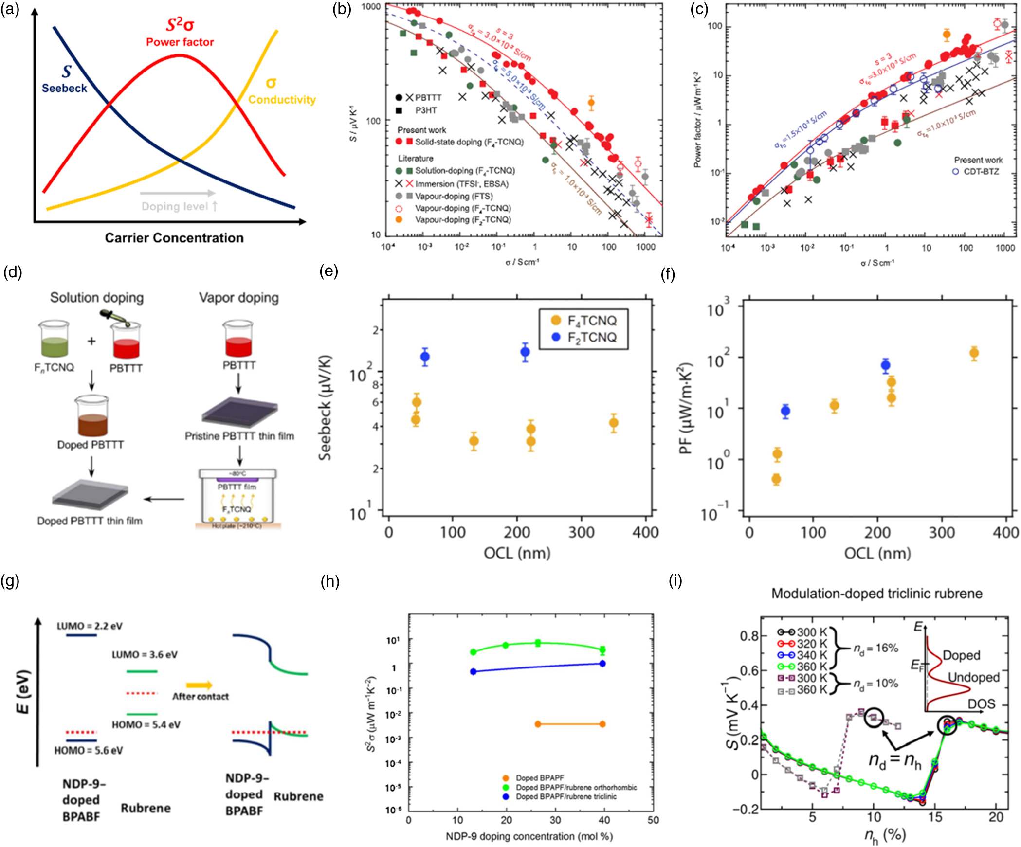
The most effective doping method in OSC is controlling charge carrier concentration without compromising carrier mobility. Considering this, it is important to develop a doping method that provides free electrons and holes efficiently and retains the molecular arrangement of an OSC designed for high charge mobility. From this point-of-view, the solid-state diffusion method discussed above is one of the best doping methods. It has been reported that solid-state diffusion methods can maintain the morphology of the PBTTT while minimizing the structural disorder caused by the dopants and maximising conductivity through high doping efficiency, leading to a high power factor. 92) By comparing with the solution-doped sample (i.e. co-deposition method), the retained orientational correlation length (OCL) was discovered to be the key to improving electrical conductivity and charge mobility without loss of the Seebeck coefficient [Figs. 10(e), 10(f)]. 92,96)
Recently, Wang et al. demonstrated that modulation doping of orthorhombic rubrene can be realised for achieving superior doping efficiency even at high doping density, which leads to thermoelectric power factors over 20 μWm−1 K−2 at 80 °C. 59) The advantage of avoiding physically separating ionized dopant molecules from the transport channel for minimizing Coulomb scattering can be attributed as the origin for achieving both a high carrier concentration and mobility, which leads to higher power factor values [Figs. 10(g) and 10(h)]. Orthorhombic rubrene showed 2.7 to 7.6 μWm−1 K−2 of power factor at the doping concentration range from 13 to 39 mol%, and the power factor of triclinic rubrene crystals was increased from 0.48 to 0.99 μWm−1 K−2 by increasing doping concentration from 13 to 39 mol%. These power factor values obtained by modulation doping are much higher than those of bulk-doped 9,9-bis[4-(N,N-bis-biphenyl-4-yl-amino)phenyl]-9H-fluorene (BPAPF) with the value of 3.5 × 10⁻³ μWm−1 K−2 even at high doping levels (∼39 mol%). The authors also investigated the charge transport mechanism by measuring temperature-dependent Seebeck coefficient of modulation-doped rubrene crystals. Triclinic rubrene crystals showed an unusual temperature dependence expected for Seebeck coefficient, with the Seebeck coefficient decreasing with increasing temperature, while the Seebeck coefficient of orthorhombic rubrene crystals increased as the temperature increased. This unexpected behaviour can be attributed to the different energetic bandwidth and density of states (DOS) between the doped triclinic and orthorhombic rubrene crystals [Figs. 10(i)], indicating that an enhanced electronic coupling (broader bandwidth and smaller width of a local minimum in DOS) leads to the increase in the Seebeck coefficient with increasing temperature.
3. Conclusion and outlook
In this review, we introduced the molecular doping of organic semiconductors and comprehensively summarised the established doping mechanism, dopant materials, doping methods, and its device applications. Discussion on the doping mechanism and brief guidelines for differentiating the mechanism of doping based on experimental and phenomenological bases is outlined. Various dopant molecules are also shown as representative molecular designs for achieving efficient doping of target organic semiconductors. The doping method is also critical to realize efficient doping without generating dopant-induced disorder, therefore, we discussed the feature of various doping methods developed in the field for achieving efficient molecular doping and correlate their impacts on device applications to develop insights for better understanding the role of molecular doping in various devices such as OFETs, OTEs, and OPVs.
Molecular doping of OSCs is one of the critical themes in organic electronics these days in terms of its universality, impact on the field, and diversity of its application. Therefore, there is a continuous effort in the field for advancing doping methods, molecular designs, and investigating the relevant mechanism of doping. In particular, fundamental understanding of molecular doping process and its effect on charge transport in OSCs may be the key to the breakthrough of organic electronics, leading to the selection of the best dopant−semiconductor combination. In this aspect, recent works that feature the role of paracrystalline disorder in charge transport provide structural guidance for designing highly conducting polymers, which has to be pursued intensively in the field. 97,98) Last but not least, although p-type doping has been predominantly discussed for device applications, n-type doping deserves significant attention due to challenges in simultaneously attaining both high-mobility n-type semiconducting host 99) and strong n-type dopants 100) without compromising their chemical stability in air (see Fig. 4 for energetic requirements). Especially, n-type conductors that show on par performance with p-type conducting polymers would overcome one of the critical limitations currently limiting organic thermoelectrics. 95)
Overall, further concerted efforts in the field to unveil the above unexplored aspects of molecular doping will accelerate the commercialization and utilization of various organic electronics such as OFETs, OTEs, and OPVs in practical applications. We believe that this review can provide deep insight into developing new doping techniques and suggest an innovative direction for organic next-generation electronics.
Acknowledgments
The authors appreciate the financial support of the National Research Foundation of Korea (NRF) grant (No. 2021R1C1C1010266), the Nano•Material Technology Development Program Grant (No. 2021M3H4A1A02049651), the BrainLink program (No. 2022H1D3A3A01077343) through NRF funded by the Ministry of Science and ICT of Korea and the New Faculty Startup Fund from Seoul National University.