
Abstract
This paper proposes a switched-capacitor voltage buck converter (SC-VBC) with variable step-down controller (VSC) and switching frequency controller (SFC). The VSC and SFC change the step-down ratio and switching frequency of the SC-VBC in accordance with the input voltage and load current, respectively, enabling the converter to operate efficiently with a wide-ranging input voltage and load current. Measurements of a prototype chip demonstrated that our SC-VBC achieved a wide input voltage range and high efficiency of 1.3–2.6 V and 69%, respectively.
Export citation and abstract BibTeX RIS
1. Introduction
Energy harvesting and power management techniques have been developed towards battery- and maintenance-free autonomous IoT (Internet-of-Things) devices. 1–13) Intermittent power management systems, shown in Fig. 1, are widely used to operate application circuits and systems stably because the output voltages of small energy harvesters are usually low and easily lost. 14–22) The systems store surplus energy in a storage battery 23) and use it as needed. The stored energy must be regulated to a certain voltage (e.g. 1.0- or 1.2 V power supplies for 65 nm CMOS technology) because the battery's voltage is higher than the voltage for the application circuits. For an efficient step-down voltage conversion, a switching voltage buck converter (VBC) can be used as an intermediate building block between the battery and a linear voltage regulator because the power loss in the regulator increases when the voltage difference between the input and the output becomes large. The VBC once converts a battery voltage to a lower voltage, which is 100 mV higher than the output voltage, and the regulator generates a supply voltage for the application circuits (e.g. the regulator converts from 1.3–1.6 to 1.2 V).
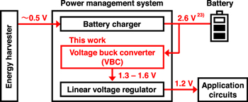
Fig. 1. (Color online) Block diagram of the intermittent power management system.
Download figure:
Standard image High-resolution imageThe advantage of a switched-capacitor VBC (SC-VBC) is that it can efficiently convert a voltage and be fully integrated on a chip without any external components. 24–31) However, there are problems with the conventional SC-VBC. First, when the step-down ratio of the SC-VBC is fixed, the usable input voltage from the storage will be limited to a narrow range. 25,31) For example, when a converter is designed with a fixed step-down ratio of 5/8, the lowest input voltage for the SC-VBC will be 2.1 V (2.1 × 5/8 = 1.3 V). If the voltage drops below 2.1 V, the regulator followed by the converter cannot generate a 1.2 V output voltage correctly. Second, the charge transfer capability of the SC-VBC depends on the capacitors and switching frequency. 10,11) Thus, it becomes difficult for the converter to supply a wide load current efficiently under the area-limited on-chip capacitors.
In light of this, we propose a SC-VBC with variable step-down controller (VSC) and switching frequency controller (SFC). The VSC and SFC change the step-down ratio and the switching frequency in accordance with the input voltage and load current, respectively, enabling the converter to operate efficiently with a wide range of input voltages and load currents. In contrast to our previous work, 32) here, we add some simulation results and discuss its circuit operation in more detail. In addition, we also describe an output voltage monitor (OVM), which stops the SC-VBC operation when the output voltage is fully charged, for preventing unnecessary power loss in the SC-VBC.
This paper is organized as follows. In Sect. 2, we present our proposed SC-VBC and its operation. In Sect. 3, we discuss the simulation results of our proposed circuit. In Sect. 4, we show the measurement results of our prototype chip using 65 nm CMOS process technology. In Sect. 5, we conclude the paper.
2. Proposed SC-VBC
Figure 2 shows a block diagram of our proposed SC-VBC. The converter consists of a local VDD generator (LVG), 33) variable step-down controller (VSC), switching frequency controller (SFC), variable step-down SC-VBC, load current monitor (LCM), and output voltage monitor (OVM). As a basic topology of the variable step-down SC-VBC, we adopt a recursive topology for the SC-VBC. 25) Although the topology has a relatively large parasitic capacitor and needs an output filtering capacitor at each stage, it can easily generate multiple step-down ratios by properly choosing connections at each stage. The VSC monitors the input voltage VIN and changes the step-down ratio of the variable step-down SC-VBC depending on VIN. Therefore, the converter can obtain a wide input voltage range. The SFC monitors the load current with the LCM and changes the switching clock frequency for the variable step-down SC-VBC. When the load current is low, the SFC makes the frequency low to save power consumption because high charge transfer capability is not required. On the other hand, when the load current is high, the SFC makes the frequency high to convert voltage efficiently over a wide load current range. In addition, the OVM is used to stop the clock frequency for the variable step-down SC-VBC when the output voltage of the converter is sufficiently charged. The LVG generates a low supply voltage VDDL to reduce the power consumption of the SFC. 34–37) Note that the control signals of Clock and Reset are obtained from the MCU, and the voltages of VDD and VREF are obtained from other reference circuits in this work.

Fig. 2. Block diagram of proposed SC-VBC.
Download figure:
Standard image High-resolution imageAlthough the basic topology of variable step-down SC-VBC has already been reported, 25) the novelty of this work is in the combination of the VSC and SFC. It simultaneously leads to a wide input voltage and load current operation of the converter, depending on the change in VIN and IOUT.
2.1. Variable step-down SC-VBC and ratio control
The variable step-down SC-VBC utilizes a basic SC converter. Figure 3 shows a schematic of the converter. It consists of a capacitor CF, four switches, and switching driver circuits (not shown in this figure). We obtain the output voltage VOUT from the inputs VHIGH and VLOW. When SW1-SW4 and SW2-SW3 are set to On and Off, respectively, the CF is charged with VHIGH − VOUT. After that, as all switches toggle, the CF is charged with VOUT − VLOW. According to the charge conservation law, we obtain

From Eq. (1), VOUT can be rewritten as

Thus, the basic SC converter generates half of the input voltages. By using multi-stage SC converters, we can realize other fractional step-down ratios. 25,31) When we use nth-stage SC converters, we obtain 2n fractional step-down ratio (i.e. VOUT = 1/2n , 2/2n , 3/2n , ⋯ ,2n /2n ).
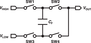
Fig. 3. Schematic of basic SC converter.
Download figure:
Standard image High-resolution imageIn this work, we use three-stage SC converters to operate the converter in a wide range of input voltages. With the configuration, we can generate eight different fractional step-down ratios.
Figure 4 illustrates the relation between the input and output voltages of the SC-VBC. In this work, we set a required output voltage range of 1.3–1.6 V. With this range, the input voltage is limited to 2.1 V when we use an SC-VBC with a fixed step-down ratio of 5/8, as discussed in Sect. 1. On the other hand, the input voltage can be reduced to as low as 1.3 V when we use four step-down ratios of 5/8, 6/8, 7/8, and 8/8, out of eight possible step-down ratios in our proposed variable step-down SC-VBC.
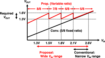
Fig. 4. (Color online) Relation between input and output voltages of proposed SC-VBC.
Download figure:
Standard image High-resolution imageFigure 5 shows a block diagram of the variable step-down SC-VBC. It consists of three basic SC converters (Fig. 3), load capacitors CL, switching MOSFETs, and transmission gates. With this configuration, we can obtain the four step-down ratios of 5/8, 6/8, 7/8, and 8/8. Table I summarizes the VIN range, step-down ratio, and corresponding control signals of S 〈3: 0〉. Figure 6 shows simplified block diagrams of the variable step-down SC-VBCs for the four step-down ratios: 5/8 [Fig. 6(a)], 6/8 [Fig. 6(b)], 7/8 [Fig. 6(c)], and 8/8 [Fig. 6(d)], respectively. The output voltages of each stage are also shown in the figure.

Fig. 5. Schematic of proposed variable step-down ratio SC-VBC.
Download figure:
Standard image High-resolution image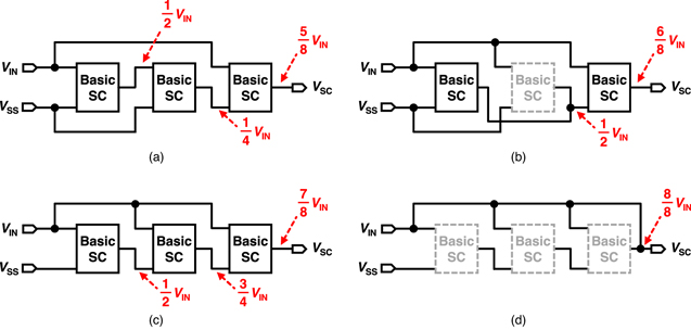
Fig. 6. (Color online) Simplified block diagrams of variable step-down SC-VBCs for step-down ratios: (a) 5/8, (b) 6/8, (c) 7/8, and (d) 8/8.
Download figure:
Standard image High-resolution imageTable I. Step-down ratios and corresponding control signals.
| VIN | Ratio | S 〈3〉 | S 〈2〉 | S 〈1〉 | S 〈0〉 |
|---|---|---|---|---|---|
| 2.1–2.6 V | 5/8 | Low | Low | Low | Low |
| 1.8–2.1 V | 6/8 | Low | Low | High | High |
| 1.5–1.8 V | 7/8 | Low | High | High | Low |
| 1.3–1.5 V | 8/8 | High | High | High | Low |
The control signals of S〈3: 0〉 are generated by the VSC. Figure 7 shows a block diagram of the VSC. It is based on a flash ADC (analog-to-digital converter). The VSC consists of resistive dividers, comparators, and an encoder. The resistive dividers generate a voltage of α · VIN, where α (<1) is a scale factor, and three reference voltages of VREF1, VREF2, and VREF3. The comparators accept these voltages and convert α · VIN to corresponding three-bit digital codes. With the digital codes, the encoder generates control signals of S〈3: 0〉 for the variable step-down SC-VBC.
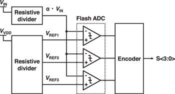
Fig. 7. Block diagram of variable step-down controller (VSC).
Download figure:
Standard image High-resolution image2.2. Switching frequency control
As discussed in Sect. 1, the charge transfer capability of the variable step-down SC-VBC is low and, in addition, the power loss should be minimized when the output voltage reaches a desired voltage and when no-load current is supplied during intermittent operation. These can be improved by switching frequency control.
Figure 8(a) shows a block diagram of the SFC. It consists of an LCM, current control oscillator (CCO), and OVM. The LCM generates a current ICCO that is proportional to the load current IOUT. The CCO receives the ICCO and generates a switching frequency that is proportional to the IOUT for the converter. The OVM monitors the output voltage of the converter VSC and generates a control signal DIS to stop the clock generation of the CCO when the VSC reaches a desired voltage. Figure 8(b) illustrates the operation of the switching frequency control.

Fig. 8. (Color online) (a) Block diagram and (b) operation of switching frequency controller (SFC).
Download figure:
Standard image High-resolution imageFigure 9 shows a schematic of the LCM. 38) It consists of pMOSFET and nMOSFET current mirrors and an amplifier with a feedback nMOSFET. The gains of the pMOSFET and nMOSFET current mirrors are set to 1:K1 and K2:1, respectively, as shown in Fig. 9. The amplifier and the feedback nMOSFET are used to improve the accuracy of the pMOSFET current mirror. The ICCO can be expressed as

The ICCO is proportional to the IOUT. Note that the LCM can also be turned off by the control signal DIS.

Fig. 9. Schematic of load current monitor (LCM). 38)
Download figure:
Standard image High-resolution imageFigure 10 shows a schematic of the CCO. It consists of a ring oscillator using current-starved inverters. The delay time of the inverter can be expressed as

where CINV is the capacitance of the inverter. From Eq. (4), the oscillation frequency with nth-stage inverters can be expressed as

As shown in Eq. (5), the switching frequency can be controlled by the ICCO. The oscillation of the CCO can be controlled by the control signal DIS.

Fig. 10. Schematic of the current controlled oscillator (CCO).
Download figure:
Standard image High-resolution imageFigure 11 shows a schematic of the OVM. It consists of a resistive divider and a hysteresis comparator. 39) The comparator compares a divided voltage VCMP with the reference voltage VREF and generates a control signal DIS to prevent unnecessary power loss in the variable step-down SC-VBC.

Fig. 11. Schematic of output voltage monitor (OVM).
Download figure:
Standard image High-resolution image3. Simulation results
We designed and evaluated our proposed SC-VBC using 65 nm CMOS process technology. We used MIM capacitors CF and CL and set them to 100 pF. The total capacitance was 900 pF. In this design, we set VDDL, VREF1, VREF2, VREF3, α, K1, and K2 to VIN/4, 1.1, 0.9, 0.8 V, 1/2, 200, and 5, respectively.
Figure 12 shows the simulated VOUT as a function of the VIN with different IOUTs of 0 and 50 μA. The proposed circuit was able to change the step-down ratio depending on VIN. The output voltage decreased as the load current increased. Note that, the voltage reduction increased as the step-down ratio increased except for the ratio of 8/8. This was because the output impedance of the multi-stage step-down SC-VBC increased as the step-down ratio increased. 11)
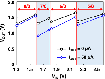
Fig. 12. (Color online) Simulated output voltage as a function of input voltage at IOUT = 0, 50 μA.
Download figure:
Standard image High-resolution imageFigure 13 shows the simulated efficiency as a function of the VIN with different IOUTs of 25 and 50 μA. The efficiency decreased significantly when the step-down ratio was 7/8. This was because the output impedance was the largest at the step-down ratio, as discussed in Fig. 12. When the step-down ratio was 6/8, the efficiency was improved compared with those at the step-down ratios of 7/8 and 5/8. This was because the second stage of the variable step-down SC-VBC was not used as shown in Fig. 6(b) and the power loss at the stage could be reduced.

Fig. 13. (Color online) Simulated efficiency as a function of input voltage at IOUT = 25, 50 μA.
Download figure:
Standard image High-resolution imageFigure 14 shows the simulated efficiency as a function of the IOUT with different VINs of 2.0 and 2.4 V. The step-down ratio was set to 6/8 and 5/8, respectively. Our proposed SC-VBC could keep high efficiency in the wide IOUT range of 0–200 μA thanks to the SFC. The maximum efficiency was 81.3% when VIN and IOUT were 2.0 V and 10 μA, respectively.

Fig. 14. (Color online) Simulated efficiency as a function of load current at VIN = 2.0, 2.4 V.
Download figure:
Standard image High-resolution image4. Experimental results
We fabricated a prototype chip of our proposed SC-VBC using 65 nm CMOS process technology. We set CF and CL to 40 pF. The CF was smaller than the simulation condition. This was because the chip area was limited and the large capacitors cannot be used in this design. Figure 15 shows a micrograph of our chip, which has an area of 0.365 mm2. We used the oscilloscope, Keysight MSO9254A, for output waveform measurements and the semiconductor device analyzer, Keysight B1500A, for other measurements.

Fig. 15. (Color online) Chip micrograph.
Download figure:
Standard image High-resolution imageFigure 16 shows the measured waveforms at VIN = 2.4 V. In this case, the step-down ratio was controlled to 5/8. The measured output voltage VOUT, ripple voltage ΔVRipple, and switching clock frequency were 1.24, 0.25 V, and 4.3 kHz, respectively. The VOUT was lower than the target voltage of 1.5 V because the output waveform was obtained by the oscilloscope with passive probes, which has an input impedance of 2.2 MΩ. In addition, the ΔVRipple was relatively large because the switching frequency was low due to the light load condition. When the load current increased to 25 μA, the switching frequency and ΔVRipple became 380 kHz and 3.0 mV, respectively.
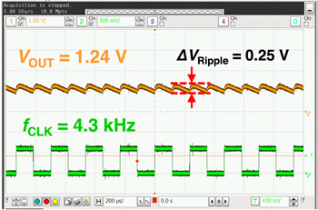
Fig. 16. (Color online) Measured waveforms at VIN = 2.4 V.
Download figure:
Standard image High-resolution imageFigure 17 shows the measured VOUT as a function of the VIN (Prop.) at IOUT = 0 A. For comparison, we also plotted the results with a fixed ratio of 5/8 (Conv.). The proposed circuit changed the step-down ratio depending on VIN. Therefore, Prop. could keep a higher output voltage than 1.3 V in a wide VIN range.

Fig. 17. (Color online) Measured output voltage as a function of input voltage at IOUT = 0 A.
Download figure:
Standard image High-resolution imageFigure 18 shows the measured clock frequency as a function of the IOUT at VIN = 2.4 V. The frequency increased in proportion to the load current from 4.3 kHz to 1.84 MHz.
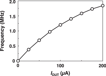
Fig. 18. Measured switching frequency as a function of load current at VIN = 2.4 V.
Download figure:
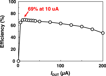
Standard image High-resolution imageFigure 19 shows the measured efficiency as a function of the IOUT. The VIN and step-down ratio were set to 2.4 V and 5/8, respectively. Our proposed SC-VBC could keep efficiency high in the wide IOUT range of 0–200 μA. The maximum efficiency and power density were 69% and 427 μW mm−2, respectively.
Fig. 19. (Color online) Measured efficiency as a function of load current at VIN = 2.4 V.
Download figure:
Standard image High-resolution image
Table II summarizes the performances of our proposed SC-VBC and other SC-VBCs. 25,29–31,40–43) For a fair comparison, we compared our proposed SC-VBC with fully on-chip SC-VBCs capable of step-down ratio control. 25,31,41) The proposed circuit has the widest VIN range of 1.3–2.6 V. It also achieves higher efficiency of 63.1% at IOUT = 100 μA, which is a target load condition of this work. Thus, our proposed circuit is useful for low-power IoT devices.
Table II. Performance summary of SC-VBCs.
| References | This work | 29 | 30 | 31 | 25 | 40 | 41 | 42 | 43 |
|---|---|---|---|---|---|---|---|---|---|
| Process [nm] | 65 | 130 | 130 | 180 | 250 | 65 | 28 | 65 | 65 |
| Area [mm2] | 0.365 | 0.218 | 1.82 | 1.69 | 4.645 | 0.3 | 1.05 | 3.18 | 2.42 |
| CTOTAL [nF] | 0.36 | 0.336 | 0.8 | 2.24 | 3.0 | 3.0 | 9.5 | 400 | 14 |
| Fully on-chip | Yes | Yes | Yes | Yes | Yes | Yes | Yes | No | Yes |
| Ratio control | Yes | No a) | No | Yes | Yes | No a) | Yes | No a) | No a) |
| Frequency control | Yes | No | Yes | Yes | Yes | No | No | No | No |
| # of ratio | 4 | 3 | 1 | 20 | 15 | 4 | 44 | 4 | 24 |
| VIN [V] | 1.3–2.6 | 1.0 | 2.7–3.3 | 3.4–4.3 | 2.5 | 2.0–2.5 | 2.0 | 1.5 | 0.22–2.4 |
| VOUT [V] | 1.3–1.6 | 0.3–0.6 | 1.05 | 0.9–1.5 | 0.1–2.2 | 0.6–1.8 | 0–2.22 | 0.18–1.19 | 0.85–1.2 |
| Max. IOUT [A] | 200 μ | 80 μ | 100 μ | 300 μ | 8.0 m | 4.0 m | 3.1 m | 400 m | 80.1 m |
| Efficiency [%] @IOUT = 100 μA | 63.1 | Cannot operate | 61 | 59 | 85 | N/A | 46 | N/A | N/A |
a)Only switched step-down ratios by an external signal, no control function.
5. Conclusion
We proposed an SC-VBC with a variable step-down ratio and switching frequency controllers. The controllers enable the SC buck converter to operate efficiently with wide ranges of input voltage and load current. The measurement results demonstrated that our SC buck converter achieved a wide input voltage range and high efficiency of 1.3–2.6 V and 69%, respectively.
Acknowledgments
This work was supported through the activities of VDEC, the University of Tokyo, in collaboration with Cadence Design Systems and Mentor Graphics. This work was also partly supported by JSPS KAKENHI Grant Numbers 20H00606, 22H03558, and JST Grant Number JPMJPF2106.