
Abstract
This paper proposes a fully-integrated switched-capacitor voltage boost converter with a digital maximum power point tracking (MPPT) control circuit for low-voltage and low-power energy harvesting. The proposed digital MPPT control circuit converts the analog voltage information of a PV cell into digital values and extracts the maximum power regardless of the harvester conditions and load current. Measurement results demonstrated that our proposed circuit can track the maximum power point of a PV cell successfully. The maximum voltage conversion ratio of our circuit was 5.6. The proposed power management system generated a 2.58 V output voltage from a 0.46 V input voltage. The maximum power conversion efficiency was 63.6%.
Export citation and abstract BibTeX RIS
1. Introduction
Internet-of-things (IoT) devices must be small, low-cost, maintenance-free, and operate at ultra-low power. 1–11) Energy harvesting has attracted attention as an alternative energy source for such devices, instead of using small chemical batteries. 12,13) Among the several harvesters, photovoltaic (PV) cells are some of the most common and practical ones because they can generate electricity from surrounding ambient light, not only sunshine but also indoor light. 14,15) However, the output voltage of a single PV cell is as low as 0.6 V or less, depending on the environmental light intensity. This voltage is too low to charge energy storage devices (e.g. secondary batteries such as lithium-ion batteries and supercapacitors) and drive application circuits directly. In addition, the output voltage of a small-size PV cell is basically weak and easily lost. Therefore, a highly efficient power management system (PMS) is required to develop such systems that use a small PV cell.
Figure 1 shows a block diagram of a PMS. 16–20) The PMS consists of a PV cell, switched-capacitor (SC) voltage boost converter (VBC), maximum power point tracking (MPPT) control circuit, secondary battery, and application circuits. The MPPT enables the PV cell to operate at its maximum power point (MPP). Several PMSs using MPPT have been studied. 16–24) The hill climbing MPPT architecture is widely used to maximize the output power. 17–21) In the architecture, we have to compare the PV cell's operating voltage with the voltage at the MPP. These voltages are stored and held on capacitors, and they require a large silicon area when being fabricated in an LSI chip, to suppress and minimize the effect of the leakage current of the capacitor and MOSFET switches connected to them.
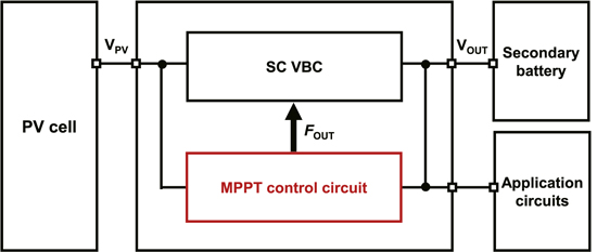
Fig. 1. (Color online) Block diagram of power management system.
Download figure:
Standard image High-resolution imageIn light of this, we present a PMS circuit with a digital MPPT control circuit. In contrast to our previous work, 25) we discuss its circuit operation and analyze its effectiveness in more detail. The proposed digital MPPT control circuit converts analog voltages into digital values to suppress and minimize the effect of leakage current. The advantage of our proposed circuit is that it can preserve voltage information as digital codes for a long time. The leakage problems can be solved by the proposed digital MPPT architecture.
This paper is organized as follows. In Sect. 2, we describe the operation of the SC VBC. In Sect. 3, we explain the operation of MPPT control. In Sect. 4, we present the operation of our proposed digital MPPT control circuit. In Sect. 5, we discuss the simulation and measurement results of our prototype chip. In Sect. 6, we conclude the paper.
2. SC VBC
Figure 2 shows a schematic of a basic SC VBC. The SC VBC consists of a capacitor CF and switches. The switches are driven by non-overlap clock signals. The SC VBC accepts input voltages VIN, VH, and VL and generates an output voltage VOUT. When SW1 and SW2 are ON and OFF, CF is charged with VIN − VL and the charge QF1 stored in the capacitor is expressed as

After that, when SW1 and SW2 toggle, CF is charged with VOUT − VH and the charge QF2 is expressed as

From the charge conservation equation, or QF1 = QF2, the output voltage VOUT can be given by

In this way, we can obtain a higher output voltage (e.g. when we set VH = VIN and VL = 0, VOUT = 2VIN can be obtained). However, the VOUT is disconnected from CF when SW2 is OFF. This causes the output voltage to reduce. To cope with the voltage reduction, a complementary circuit configuration is generally used. Figure 3 shows a schematic of the complementary circuit configuration including a load capacitor CL. The complementary block is added to Fig. 2.

Fig. 2. Schematic of SC VBC.
Download figure:
Standard image High-resolution image
Fig. 3. Schematic of complementary SC VBC.
Download figure:
Standard image High-resolution imageMulti-stage SC VBCs are widely used to convert a low input voltage to a high output voltage. Figure 4 shows a three-stage SC VBC. By connecting three SC VBCs in cascade, we can easily obtain a higher output voltage. As discussed in Eq. (3), the output voltages of the 1st, 2nd, and 3rd stages are given by 2 × VIN, 3 × VIN, and 6 × VIN, respectively. Note that, there are four possible ways to obtain 6 × VIN because we can use intermediate output voltages at each stage as VH and VL. 26) We choose the topology shown in Fig. 4 because it has the smallest output impedance. 26)
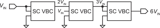
Fig. 4. Block diagram of SC VBC.
Download figure:
Standard image High-resolution image3. MPPT control circuit
3.1. MPP of PV cell
Figure 5 illustrates the characteristics of a PV cell. The maximum power  of a PV cell is given by

where VMPP and IMPP are the MPP voltage and current of the PV cell, respectively. The MPP voltage VMPP is defined as

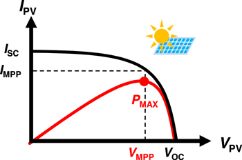
Fig. 5. (Color online) Characteristics of PV cell.
Download figure:
Standard image High-resolution imageTo extract the maximum power  , the PV cell must operate at the MPP, or at VMPP and IMPP. To realize MPPT operation, we have to develop an MPPT control circuit.
3.2. MPPT control
The MPPT control maximizes the output power of the PV cell. As discussed in previous research, 26) the impedance ZSC of the SC VBC is expressed as

As shown in Eq. (6), the ZSC depends on the clock frequency FOUT of the SC VBC. Therefore, the operating point of PV cells can be controlled by changing the frequency FOUT of the SC VBC. The MPPT control circuit controls the frequency FOUT so that the operating voltage of the PV cell becomes 80% of the open circuit voltage VOC. 27)
Figure 6 shows the operation of MPPT control. When the operating voltage VPV of the PV cell is lower than the MPP voltage VMPP, the MPPT control circuit makes the clock frequency FOUT low. This causes the ZSC to increase and then IPV to decrease. As a result, the VPV increases and approaches VMPP. On the other hand, when the operating voltage VPV is higher than the MPP voltage VMPP, the MPPT control circuit makes the clock frequency FOUT high. This causes the ZSC to decrease and then IPV to increase. As a result, the VPV decreases and approaches VMPP.
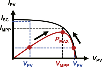
Fig. 6. (Color online) Operation of MPPT control.
Download figure:
Standard image High-resolution imageThrough the above operation, the MPPT control makes the PV cell operate at the MPP by controlling the clock frequency.
3.3. Problems with conventional MPPT control circuit
Figure 7 shows a schematic of a sample and hold (S&H) circuit and comparator used in the conventional MPPT control circuit. 17–20) Capacitors CSH1 and CSH2 in the S&H circuit hold analog voltages VSH1 and VSH2. However, the voltages stored on the capacitors decrease due to leakage currents in the capacitors and MOSFET switches.
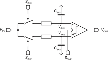
Fig. 7. Schematic of sample and hold (S&H) circuit and comparator used in conventional MPPT control circuit. 17–20)
Download figure:
Standard image High-resolution imageFigure 8 illustrates waveforms and timing charts with and without the effect of leakage currents, respectively. The VPV is sampled twice with SSH1 and SSH2, and then these voltages are compared with SCMP by the comparator. As shown in Fig. 8(a), the sampling voltages stored on the capacitors are kept constant if the leakage currents can be ignored, and the comparator gives a correct comparison result. However, the voltages stored on CSH1 and CSH2 decrease with time, as shown in Fig. 8(b), and will result in a wrong comparison result in the worst case. Thus, we cannot ignore the leakage problems in actual circuit design.
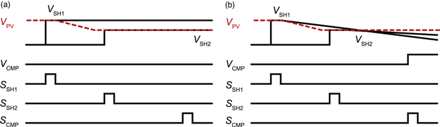
Fig. 8. (Color online) Illustration of PV cell's voltage VPV and control signals of proposed MPPT control circuit, (a) without and (b) with effect of leakage.
Download figure:
Standard image High-resolution image4. Proposed MPPT control circuit
4.1. MPPT control circuit
Figure 9 shows a block diagram of our proposed digital MPPT control circuit. The circuit consists of a voltage-to-frequency converter (VFC), two 10 bit counters (UCNT0/1), a digital comparator, timing controller, successive approximation register (SAR), and digital RC oscillator (RC OSC). The VFC is made up of an SC voltage buck converter (SC4/5), multiplexer, and ring oscillator circuit (RING OSC). The SC4/5 generates a voltage that is 80% of the open circuit voltage of the PV cell and is suitable for this PMS because it is easy to integrate and low power consumption can be expected. 28–30) In the following, we explain the operation of our proposed MPPT control circuit.
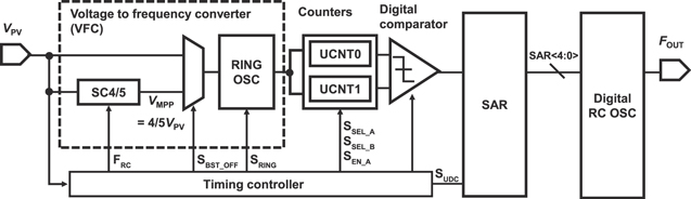
Fig. 9. Block diagram of proposed MPPT control circuit.
Download figure:
Standard image High-resolution image4.2. Operation of MPPT control circuit
First, the MPPT control circuit digitizes a PV cell's MPP voltage and stores the information on UCNT0 as follows. The open circuit voltage of the PV cell is applied to the SC4/5, and then we obtain the PV cell's MPP voltage. The voltage is used as a supply voltage for the RING OSC and generates a frequency. UCNT0 receives the frequency and stores the digital information of the MPP.
Next, the SAR determines the appropriate operating frequency FOUT. We set the most significant bit (MSB) in the SAR to high and all other bits to low. The digital RC OSC receives the code and generates an operating frequency FOUT to drive the SC VBC. The operating voltage VPV of the PV cell is sampled and is also used as a supply voltage for the RING OSC in the VFC. The RING OSC generates a frequency from the VPV. UCNT1 receives the frequency and stores the digital information of the operating point of the PV cell. The digital comparator compares the stored values in UCNT1 with those in UCNT0, and then the MSB in the SAR is updated on the basis of the comparison result.
The lower bits of the SAR are also updated by repeating the above comparison procedure. In this way, the registers in the SAR are determined so that the count value of UCNT1 becomes equal to that of UCNT0.
A flow chart for the proposed SAR MPPT algorithm is shown in Fig. 10. The output frequency of the digital RC OSC is controlled by the SAR output code. By updating the frequency sequentially, the desired frequency can be obtained.

Fig. 10. Flow chart for proposed MPPT algorithm.
Download figure:
Standard image High-resolution image4.3. Digital RC oscillator
Figure 11 shows a schematic of the digital RC OSC. It consists of resistors, variable capacitors, switches, and control logic gates. The frequency of the digital RC OSC can be expressed as 31)

The frequency can be controlled by changing the RC product with the SAR digital codes and logic gates. Note that, when we sample and hold an open circuit voltage VOC of the PV cell, we set SBST_OFF low to stop the converter operation.

Fig. 11. Schematic of digital RC OSC.
Download figure:
Standard image High-resolution image4.4. Timing controller
Figure 12 shows a block diagram of the timing controller. The controller generates control signals for the proposed MPPT control circuit shown in Fig. 9. The controller consists of an RC oscillator (RCOSC), frequency divider, and control signal generator. The frequency divider and control signal generator are composed of D flip-flops (DFFs) and combinational logic gates. The output voltage of the PV cell VPV is used as a supply voltage for the controller.
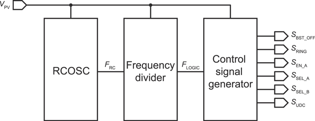
Fig. 12. Block diagram of timing controller.
Download figure:
Standard image High-resolution imageFigure 13 shows a timing chart of the MPPT control circuit. SEN_A first resets UCNT0 and UCNT1. To obtain the MPP voltage of the PV cell VMPP, SBST_OFF is asserted to stop the SC VBC operation. The MPP voltage is obtained by the SC4/5. SRING generates a frequency by the RING OSC whose supply voltage is the MPP voltage. UCNT0 receives the frequency with SSEL_A. After storing the digital information of the MPP voltage in UCNT0, SRING and SSEL_B enable UCNT1. The SAR then updates the frequency and determines the appropriate frequency with SUDC.
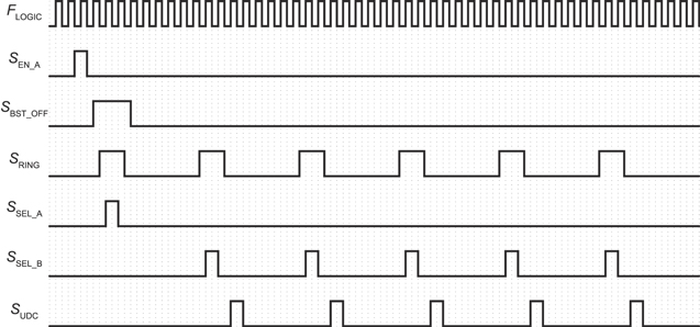
Fig. 13. Timing chart of control signal.
Download figure:
Standard image High-resolution image5. Results
5.1. Simulation results
The proposed MPPT control circuit was simulated in 0.18 μm CMOS technology with a deep n-well option. The performance of the digital RC OSC, an equivalent model of the PV cell, and operation of the proposed MPPT control circuit using the PV cell model were simulated.
Figure 14 shows the simulated frequency FOUT of the digital RC OSC. Transient performance was evaluated with incremental digital codes of SAR <4:0>. We confirmed that the output frequency increased as the codes increased. Figure 15 shows the frequency FOUT. The oscillation frequency can be controlled from 162 kHz to 4.62 MHz with digital codes.

Fig. 14. Simulation frequency with incremental SAR codes SAR <4:0>.
Download figure:
Standard image High-resolution image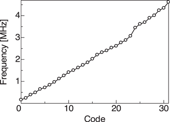
Fig. 15. Simulation frequency of digital RC OSC.
Download figure:
Standard image High-resolution imageFigure 16 shows an equivalent circuit model and the characteristics of the PV cell we used. The PV cell model was developed using a current source, diode, and shunt and series resistors. The open circuit voltage and short circuit current were 325 mV and 1.75 μA, respectively, and the maximum power was 0.40 μW.
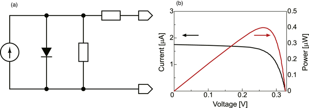
Fig. 16. (Color online) (a) Equivalent PV cell model and (b) simulated characteristics.
Download figure:
Standard image High-resolution imageFigure 17 shows simulation results for the SAR codes SAR <4:0> and the PV cell's voltage VPV. The SAR codes were determined from the MSB to the least significant bit (LSB), and the VPV settled at 281 mV, which was about 86% of the open circuit voltage VOC. This slightly deviated from 80%. The deviation can be improved by using a finer frequency step with high-resolution SAR codes.
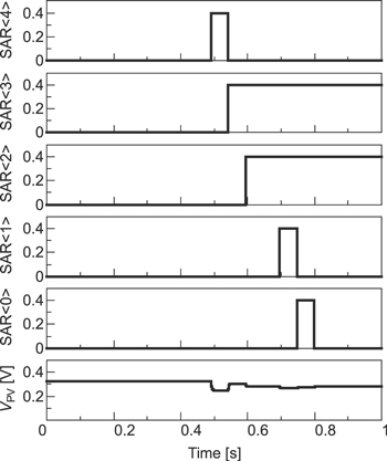
Fig. 17. Simulated SAR output codes and PV cell's voltage VPV.
Download figure:
Standard image High-resolution image5.2. Measurement results
A prototype chip was fabricated using a 0.18 μm 1P6M CMOS process with the same technology. Figure 18 shows a chip micrograph (area: 1.57 mm2). The voltage conversion ratio of the SC VBC was set to 6 in this design. Figure 19 shows the measured characteristics of the PV cell. The area of the PV cell was 1 cm2. The open circuit voltage, short circuit current, and maximum power of the PV cell, when we set the illuminance to 200 and 500 lx, were 0.58 and 0.62 V, 9.24 and 23.1 μA, and 3.71 and 10.0 μW, respectively. For the measurement, we used two commercial PV cells connected in parallel. Note that, as shown in Figs. 9 and 12, the power supply voltage of the MPPT control circuit was supplied from VPV and internal voltage which was generated by the SC VBC. In this design, we made the MPPT control circuit operate once every 3.76 s.
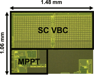
Fig. 18. (Color online) Chip micrograph of proposed circuit.
Download figure:
Standard image High-resolution image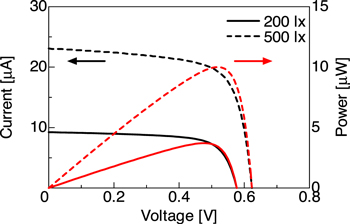
Fig. 19. (Color online) Measured characteristics of PV cell.
Download figure:
Standard image High-resolution imageFigure 20 shows the measured waveforms of the PV cell and the output voltage of the SC VBC under no load at 200 lx illuminance. As shown in the figure, the operation was divided into three periods: (1) before evaluation, (2) during evaluation, and (3) after evaluation. As shown in the after-evaluation period (Fig. 20 (3)), the PV cell's voltage VPV settled to 0.46 V, which was 80% of the open circuit voltage of 0.58 V. The output voltage of the SC VBC was 2.58 V, which was about six times higher than that of the PV cell voltage. Figure 21 shows the measured output power at 500 lx illuminance. For this measurement, a resistive load of 410 kΩ was connected to the output. The output power in the after-evaluation period (Fig. 21 (3)) increased, compared with that in the before-evaluation period (Fig. 21 (1)). This was because our proposed MPPT control circuit was able to generate an appropriate frequency for the SC VBC. The ripple of the output power increased slightly because the output impedance of the converter was reduced by increasing the frequency 26) and the output current increased. Figure 22 shows the measured voltage conversion ratio (VCR) of the proposed circuit. The VCR was higher than 5 in the load current range from 0 to 1.7 μA at 200 lx illuminance and from 0 to 3.1 μA at 500 lx illuminance. Figure 23 shows the power conversion efficiency (PCE) of the proposed circuit at 200 and 500 lx illuminance. The PCE was calculated by

where PIN, POUT, and PLOSS are the input power, output power, and power of the control circuit, respectively. The maximum PCE was 63.6% and 58.6% at 200 and 500 lx illuminance, where the PLOSS at the maximum PCE was 2.67 and 7.99 μW, respectively.
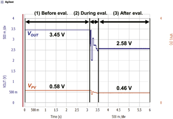
Fig. 20. (Color online) Measured PV cell's voltage VPV and output voltage of converter at 200 lx illuminance.
Download figure:
Standard image High-resolution image
Fig. 21. Measured output power at 500 lx illuminance.
Download figure:
Standard image High-resolution image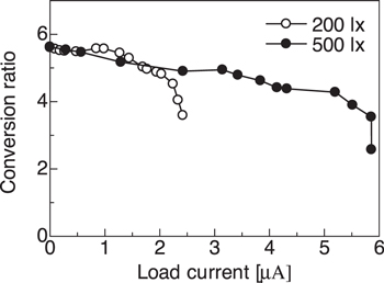
Fig. 22. Measured voltage conversion ratio (VCR).
Download figure:
Standard image High-resolution image
Fig. 23. Measured power conversion efficiency (PCE).
Download figure:
Standard image High-resolution image
Table I gives a performance summary and comparison of our MPPT control circuit and others. 32–35) Our proposed circuit achieved digital MPPT control with a fully on-chip configuration. 32) is based on the digital MPPT circuit and achieved high efficiency. However, the VCR and the output voltage were quite low. Other works 33–35) generated higher voltage to charge the secondary battery. Compared with these works, ours achieved a high VCR and PCE by using a digital MPPT circuit and highly efficient designs.
Table I. Performance summary and comparison.
| Ref. | This work | Rawy 32) | Jung 33) | Tsai 34) | Wu 35) |
|---|---|---|---|---|---|
| Technology | 0.18 μm | 65 nm | 0.18 μm | 0.18 μm | 0.18 μm |
| MPPT technique | Digital (Freq.) | Digital (Freq.) | No MPPT | No MPPT | Analog (Cap.) |
| MPPT location | VIN | VOUT | No | No | VIN |
| Input range | 0.3–0.6 V | 0.35–1 V | 0.14–0.5 V | 1 V | 0.25–0.65 V |
| Output range | 2.4–3.6 V | 1 V | 2.2–5.2 V | 3–6 V | 3.8–4 V |
| Frequency range | 162 k–4.62 MHz | 19 k–16 MHz | 70–19 MHz | 10 k–20 MHz | N/A |
| Peak efficiency | 63.6% | 83% | 50% | 58% | 60% |
| Fully integrated | Yes | Yes | Yes | Yes | Yes |
| Monolithic area | 1.57 mm2 | 0.54 mm2 | 0.86 mm2 | 0.5 mm2 | 2.72 mm2 |
6. Conclusion
We developed an SC VBC with a digital MPPT control circuit. The circuit enabled the PMS to operate with high efficiency. The measurement results demonstrated that the proposed PMS generated a 2.58 V output voltage from a 0.46 V input voltage at 200 lx illuminance. The proposed circuit achieved a maximum voltage conversion ratio of 5.6 and a power conversion efficiency of 63.6% at 2.21 μA at 200 lx illuminance.
Acknowledgments
This work was supported through the activities of VDEC, The University of Tokyo, in collaboration with Cadence Design Systems and Mentor Graphics. This work was also partly supported by JSPS KAKENHI Grant Nos. 20H00606, 22H03558, 22H04221, JST Grant No. JPMJPF2106, the Hyogo Science and Technology Association and the ICOM Foundation, Japan.