
Abstract
GaN micro-disk cavities undercut by laser-assisted photo-electrochemical (PEC) etching are fabricated and optically characterized. The laser source used in the PEC etching is tuned to be absorbed by the InGaN/GaN superlattice beneath the GaN disk to selectively etch the superlattice. Whispering gallery modes (WGMs) in fabricated GaN micro-disk cavities are evaluated by micro-photoluminescence spectroscopy of light emission from the embedded InGaN quantum wells. Quality factors estimated for the WGMs reach approximately 6700 at blue-violet wavelengths. Detailed analysis suggests that the high-Q WGMs are the fundamental WGMs. These results indicate the high applicability of laser-assisted PEC etching to the fabrication of air-clad GaN micro-cavities.
Export citation and abstract BibTeX RIS
1. Introduction
Optical cavities with small volume, or micro-cavities, 1) are an interesting platform to enhance the interaction between confined light and constituent material. Light emission and nonlinear optical processes in micro-cavities have been studied in a wide range of materials for optoelectronic and photonic device applications. 1–13) In particular, micro-cavities made of III-nitride (N) semiconductors are attractive with promising applications as light sources. 11–13) The width of the direct-transition bandgap in III-N semiconductors can be tuned by the molar ratio of the group III element. Current crystal growth technology on III-N semiconductors allows the formation of various quantum nanostructures, 14,15) such as quantum wells (QWs) or dots, which can act as efficient light emitters at various wavelengths from near-infrared to ultraviolet (UV). These material properties of III-N semiconductors are important to realize efficient light sources based on micro-cavities in a wide wavelength range.
Among various micro-cavity structures, micro-disk cavities are extensively studied because of their ease of fabrication and high-quality factors. 11,13) These simple disk-shaped cavities can strongly confine light in the form of whispering gallery modes (WGMs). Lasing oscillation and light emission enhancement have been demonstrated in various wavelengths from visible to UV using III-N semiconductor-based micro-disks. 16–27) Control of light emission directions and lowering lasing thresholds, by modification of the micro-disk design, have also been explored. 28–32) In addition, several schemes for the electrical operation of such light sources using III-N semiconductor-based micro-disk cavities have been proposed. 33–36) These works could lead to various applications such as sensors, 37,38) visible light communications, 36) and integrated light sources in photonic circuits. 39)
To strongly confine light in III-N-based micro-cavities, much work has focused on the development of fabrication techniques. 20,30,40–46) Undercut etching is a crucial technique to strongly confine light in micro-cavities with air-cladding. Previous studies have demonstrated strong light confinement in III-N-based micro-disk cavities 18,19,47–49) by a sophisticated undercut etching technique to form an air gap under the disk edge. This can suppress unintentional optical coupling of WGMs to the underlying substrate and enhances the quality factor. Among various undercut etching methods, bandgap selective photo-electrochemical (PEC) etching of InGaN/GaN superlattice (SL) 19,32,40) is a promising one. CW operation of GaN micro-disk lasers 21) and low-threshold lasing 32) at room temperature were demonstrated using this technique.
An issue in undercutting by PEC etching is the low etching selectivity. The Xe lamp previously used for selective removal of InGaN/GaN SL is a broadband light source. Thus, it can be absorbed by the constituent material of the cavity structures. This will limit the etching selectivity and possibly degrade the surface roughness when long etching times are required. In order to improve the etching selectivity, PEC etching using a laser source that is selectively absorbed by the SL, or laser-assisted PEC etching, was recently proposed. 41) However, there are few reports on the optical characterization of micro-cavities undercut by this method, making the applicability of this method to micro-cavity fabrication unclear. Recently, at an international conference, we reported that GaN micro-disk cavities undercut by laser-assisted PEC etching exhibited a WGM with a high-quality factor of 3900 in blue-violet wavelengths. 50)
In this paper, we report details on the fabrication and optical characterization of the GaN micro-disk cavities undercut by the laser-assisted PEC etching. The micro-disk structures were formed by electron-beam (EB) lithography followed by reactive ion etching, then undercut by laser-assisted PEC etching. The laser wavelength for the PEC etching is selected as the laser to be absorbed bandgap-selectively by the InGaN/GaN SL under the disk. We embedded an InGaN QW in the micro-disk and investigated the optical characteristics via micro-photoluminescence (μ-PL) spectroscopy. μ-PL spectra measured from the undercut micro-disks exhibit several sharp peaks originating from WGMs within the range of the QW light emission spectrum. Measured quality factors for the WGMs reach approximately 6700 in blue-violet wavelengths. A detailed investigation of the mode indices of the WGMs suggests that the high Q resonant modes are attributed to the fundamental WGMs. These results and analysis highlight the applicability of laser-assisted PEC etching to the fabrication of air-clad GaN micro-cavities.
2. Experimental methods
2.1. Fabrication process of GaN micro-disk cavities
For the fabrication of GaN micro-disk cavities, we used the substrate shown in Fig. 1(a) where a GaN buffer layer, InGaN/GaN SL, a GaN layer including an InGaN QW are sequentially grown on a c-plane sapphire by metal-organic chemical vapor deposition. The thicknesses of the layers are 1 μm, 300 nm, and 120 nm, respectively. In the SL, the respective thicknesses of InGaN and GaN are approximately 3 nm and 6 nm each. Figure 1(b) is a macro-PL spectrum measured for the substrate under the excitation by a CW He-Cd laser at room temperature. PL from the single QW is located at around 390 nm wavelength whilst that from the SL is around 430 nm. Circular disk patterns of diameter D are formed by reactive ion etching using Cl2 and BCl3 gas through a SiO2 hard mask defined by EB-lithography. Then, the sample is immersed in 25 percent tetramethylammonium hydroxide (TMAH) aqueous solution for 10 min at 80 °C. For PEC undercut etching, we used the setup in Fig. 1(c). The sample and a Pt electrode are soaked in a HCl aqueous solution of 0.006 M concentration under a bias voltage of 0.1 V. Laser light at 405 nm wavelength pulsed by a chopper is irradiated to the sample. The pulse width, peak power, and repetition rate are 50 μs, 5 mW, and 10 kHz, respectively. The laser, of which wavelength is longer than the light emission of the QW, but shorter than that of the SL, is bandgap-selectively absorbed in the SL. Thus, highly selective undercut etching is expected.
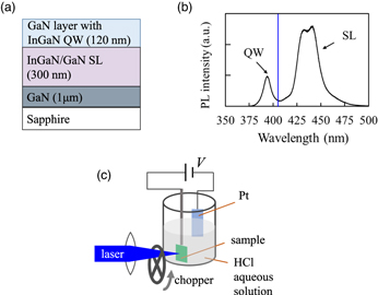
Fig. 1. (Color online) (a) Schematic of the substrate structure. (b) Macro-PL spectrum measured for the substrate. The substrate is excited by a CW He-Cd laser of 1 mW input power at room temperature. The wavelength of the laser source used for the PEC etching is shown in blue. (c) Schematic illustration of the experimental setup for the laser-assisted PEC etching.
Download figure:
Standard image High-resolution image2.2. μ-PL spectroscopy setup for optical characterization
Optical characterization is performed by μ-PL spectroscopy using CW He-Cd laser at room temperature. The excitation laser is focused on the top of the micro-disk cavities with an objective lens of 20 times magnification and 0.45 numerical aperture. The PL signal is collected by the same objective lens and measured by a spectrometer equipped with a cooled CCD array. We measured PL spectra with different resolutions. The groove density of the grating used for the low-resolution measurement is 1200mm−1 and 2400mm−1 for the high resolution.
2.3. Numerical simulation setup
For calculation of free spectral range (FSR) and modal distribution for WGMs in GaN micro-disk cavities in Sect. 3.3, we used a three-dimensional finite-difference time-domain (3D-FDTD) method. 51) The spatial mesh size is 0.01 μm × 0.01 μm × 0.01 μm. The micro-disk of D = 2.6 μm is simulated as a 120 nm thick-cylindrical disk made of GaN in air. Although the SL layer around the center of the micro-disk is left un-etched by PEC etching, it is not taken into account in our simulations. The refractive index of the GaN disk is set to 2.6. The influence of material dispersion and InGaN QW is not included.
3. Results and discussion
3.1. SEM analysis of a GaN micro-disk undercut by laser-assisted PEC etching
Figures 2(a) and 2(b) are top and side-view SEM images of an undercut GaN micro-disk for D ∼ 3 μm. The PEC etching is conducted for 30 min for this sample. From the side view, you can find that the PEC etching occurs only at the layer underneath the GaN micro-disk, which indicates the selective removal of the SL layer under the GaN disk. The edge of the GaN micro-disk has high verticality because of the TMAH process before the PEC etching. The thickness of the disk is estimated to be approximately 120 nm. In the top view image, the undercut region is bright, while the darker region around the center of the disk indicates where the SL still remains. The high-level circularity of the bright region suggests that the PEC etching proceeds homogeneously in lateral directions. The length of the PEC etching in the lateral direction is approximately 1 μm. This corresponds to the etching rate of 33 nm min−1 which is almost the same as that reported in Ref. 40 where a Xe lamp is used as the light source. The selective etching of relatively thick sacrificial layers of more than 100 nm is important for strong light confinement in GaN micro-disks. 52) These results indicate that the undercut etching of the GaN micro-disk is accomplished by our laser-assisted PEC etching.
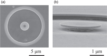
Fig. 2. (a) Top and (b) side-view SEM images of an undercut GaN micro-disk with D ∼ 3.0 μm.
Download figure:
Standard image High-resolution image3.2. Optical characterization of GaN micro-disk cavities
The red curve in Fig. 3(a) shows a measured low-resolution μ-PL spectrum for an undercut GaN micro-disk of D ∼ 3.0 μm. The spectrum for the unprocessed substrate is also shown in black. The excitation power is 4.6 μW for these measurements. Two distinct peaks are observed around 380 nm and 430 nm wavelengths for the unprocessed substrate. Through comparison with the micro-PL spectrum in Fig. 1(b), these peaks can be attributed to light emission from the QW in the micro-disk and that from the SL. In the measured spectrum for the GaN micro-disk, the PL intensity from the SL decreases due to undercutting etching of a part of the SL. Several sharp peaks are also observed in wavelengths longer than the QW emission peak. For detailed investigation, the spectral region of the peaks is magnified in Fig. 3(b). We can confirm that a few peaks periodically appear at a wavelength interval of Δλ ∼ 5.6 nm. This wavelength interval is considered the FSR of WGMs in the GaN micro-disk cavity. For the estimation of a theoretical value of the FSR, we calculate the value of the equation Δλ = λ2/(πDng), where ng is the group refractive index. This leads to Δλ ∼ 5.7 nm under the assumption of ng = 3, 21) which coincides well with the experimental one. This result indicates that the observed peaks originate from WGMs in the GaN micro-disk cavity.

Fig. 3. (Color online) (a) Low-resolution μ-PL spectra for an unprocessed substrate (black) and the GaN micro-disk cavity of D ∼3.0 μm (red). The spectrum for the black curve is scaled by a factor of 1/3 for clarity. (b) Low-resolution μ-PL spectra for the micro-disk cavities of different Ds. The blue, red, and green curves correspond to D ∼ 2.6 μm, 3.0 μm, and 3.4 μm, respectively. (c) High-resolution μ-PL spectrum for the micro-disk cavity of D ∼ 2.6 μm. The red circles are the measured PL intensity. The fitted Lorentz function for the two resonant peaks is shown in black.
Download figure:
Standard image High-resolution imageThe PL spectrum for D ∼ 3.0 μm in Fig. 3(b) also exhibits several peaks within the FSR. This result suggests that higher-order modes also exist in this cavity. For a more detailed investigation, we measured μ-PL spectra for different Ds. Blue and green curves in Fig. 3(b) show the spectra for D ∼ 2.6 μm and D ∼ 3.4 μm, respectively. As D increases from 2.6 μm to 3.4 μm, the number of peaks significantly increases. On the other hand, the theoretical FSR only varies from 6.5 nm to 5.0 nm. Thus, the increased number of peaks can mainly be due to the increase in higher-order modes.
For quantitative evaluation of the GaN micro-disk cavity, we estimate the quality factors of the WGMs by measuring the Lorentz line widths of cavity mode spectra. We observed high-quality factors for the GaN micro-disk cavity with D ∼ 2.6 μm. A measured high-resolution cavity mode spectrum is shown in Fig. 3(c). Two resonant peaks are observed at 396.2 nm and 396.6 nm wavelengths in this spectrum. Note that the background is subtracted by polynomial fitting. The fitted Lorentz function for these peaks is shown in black. The extracted line widths are 0.0589 nm and 0.0593 nm, corresponding to Q ∼ 6730 and Q ∼ 6690. These values are comparable to the highest Q-factor reported for GaN micro-disk cavities undercut by PEC etching. 19) This result suggests that undercutting by laser-assisted PEC etching can form a smooth surface at the backside of GaN micro-disk cavities. The measured line widths in Fig. 3(c) are currently limited by the resolution of our optical setup. Spectroscopy evaluation at higher resolution may result in higher Q-factors.
3.3. Radial mode index of high-Q WGMs
Although some WGMs in our GaN micro-disk cavities can exhibit high Q-factors, the characteristic mode index for these WGMs is still unclear. As discussed in Sect. 3.2, a large number of higher-order modes are included in the PL spectra observed. In the case of our thin micro-disk cavities, the observed higher order modes can be mainly attributed to WGMs of higher radial mode indices rs. In order to identify the r for high-Q WGMs, we evaluated another GaN micro-disk cavity with a shorter undercut length of Luc ∼ 0.4 μm. In our substrate, the QW light emission wavelength is shorter than that of the SL [see Fig. 1(b)]. Thus, an insufficient undercut (short Luc) can result in a large absorption loss for WGMs. However, in the case of Luc ∼ 0.4 μm, the absorption loss could be large only for r > 1 due to the difference in their spatial field distribution. In Fig. 4(a), a planar distribution of electric field energy density UE calculated for the middle of thickness is shown for a WGM of r = 1 and r = 2. The UE is strongly localized around the disk edge for r = 1. For r = 2, on the other hand, the UE is also distributed apart from the disk edge. At 0.4 μm from the disk edge, the UE for r = 1 becomes almost zero while the value is finite for r = 2 as shown in Fig. 4(b), where UE is plotted as a function of position along the radial direction. Thus, we can expect that only the fundamental WGMs are observed from the micro-disk cavity of Luc ∼ 0.4 μm.
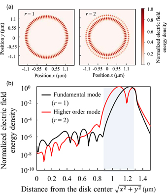
Fig. 4. (Color online) (a) Calculated planar distribution of the UE at the middle of thickness using the 3D-FDTD method for r = 1 (left) and r = 2 (right) with respect to D = 2.6 μm disk. (b) The UE as a function of the distance from the center of the disk along the radial direction. The UE is normalized so that the maximum is one for both (a) and (b). The undercut region for Luc = 0.4 μm is shown by the shaded pale blue in (b).
Download figure:
Standard image High-resolution imageFigure 5 shows PL spectra measured for micro-disk cavities of D ∼ 2.6 μm with different Lucs. The black curve is the spectrum for Luc ∼ 0.4 μm and the blue is for Luc ∼ 1 μm. For Luc ∼ 0.4 μm, we observed six resonant peaks which are labeled with numbers 1 to 6 in Fig. 5. Because of the reason discussed above, these peaks can be attributed to the fundamental (r = 1) WGMs. The wavelength interval between the peaks is 4.7 nm for modes 1 and 3, and 5.1 nm for modes 3 and 5. These values are close to the theoretical FSR in Sect. 3.2. The wavelength dependence of the FSR is likely due to the material dispersion of GaN and InGaN QW. 53,54) We also observe another resonant peak within the wavelength range of each FSR, namely the modes 2, 4, and 6 in Fig. 5. These modes appear with an FSR few percent larger than modes 1, 3 and 5. A 3D-FDTD simulation indicates that the fundamental WGMs with different polarizations exist in our micro-disk cavities. A calculated FSR for TE-like modes (dominant electric field is parallel to the disk plane) is approximately 10% larger than that of TM-like ones. Thus, the WGMs observed with slightly different FSR would be the fundamental WGMs of different polarizations. Although the polarization dependence of the FSR is slightly different between the simulation and experiment, it is likely due to the polarization dependence of InGaN QW absorption which can be stronger for TE mode than TM mode. 55) By comparing this result of Luc ∼ 0.4 μm with the spectrum for Luc ∼ 1 μm (blue curve in Fig. 5), the peak wavelengths of the fundamental WGMs for Luc ∼ 0.4 μm reasonably match with some of the peaks for Luc ∼ 1 μm. These modes can be considered as fundamental WGMs and labeled by the numbers 1' to 6' in Fig. 5. The high Q modes shown in Sect. 3.2 correspond to the modes 3' and 4', suggesting that these modes are the fundamental WGMs with different polarizations.

Fig. 5. (Color online) High-resolution μ-PL spectra measured from GaN micro-disk cavities of D ∼ 2.6 μm for different Lucs. The black and blue curves are the spectra for Luc ∼ 0.4 μm and Luc ∼ 1 μm, respectively. Coincident peaks between the spectra are labeled by n and n' for n = 1 to 6.
Download figure:
Standard image High-resolution image
4. Conclusions
We fabricate and optically characterize GaN micro-disk cavities undercut by laser-assisted PEC etching. For the PEC etching, we used a laser source of which wavelength is tuned to be absorbed bandgap-selectively by the InGaN/GaN superlattice under GaN disks. Through SEM observation, we confirm that the GaN micro-disks are successfully undercut by the PEC etching. WGMs in the undercut micro-disks are observed in the μ-PL spectra measured from the embedded InGaN QW. An estimation of the quality factors indicates that high Q-factors of approximately 6700 can be obtained at blue-violet wavelengths. We also identify the radial mode index of the high-Q WGMs through analysis of the PL spectra for the micro-disks with different undercut lengths. This result suggests that the high Q WGMs are the fundamental modes. These results highlight the applicability of the laser-assisted PEC etching to the fabrication of air-clad GaN micro-disk cavities. We believe that this technique would be useful for the improvement of other air-clad GaN micro-cavities made of III-N semiconductors.
Acknowledgments
This work was supported by JSPS KAKENHI Grant No. 20K14788 and 19K23508, the Inamori research grants program, the Amada foundation, and Yazaki Memorial Foundation for Science and Technology. The authors fabricated samples at the Division of Advanced Research Facilities (DARF) and Key Research Facilities (KRF) of the Coordinated Center for UEC Research Facilities.