
Abstract
The effect of the spreading resistance on the bileg thermoelectric generator (TEG) performance was experimentally evaluated. In planar bileg-TEGs, the width ratio of the p- and n-type legs should be carefully selected to compensate for the impedance mismatch between them and to maximize thermoelectric power generated from a unit area. In the bileg-TEG at the μm-scale, the electrical resistance becomes larger than a simple estimate using lumped parameter circuit model, which is caused by the spreading resistance; when a current flows from a narrower leg to a wider leg. A distance of greater than about 10 μm is required to distribute the electric current over the entire region of the wider leg. At shorter leg lengths, it is better to align the widths of p- and n-legs to maximize the areal power density of TEG. Decreasing the electrical resistance of the wiring between the p- and n-legs is also effective in enhancing the performance of the miniaturized TEG. The width of the p- and n-type legs in the bileg-TEG at the μm-scale should be carefully selected.
Export citation and abstract BibTeX RIS
1. Introduction
The thermoelectric (TE) energy harvesters which utilize environmental heat energies are anticipated for the portable, wearable, or swarmed sensor nodes in internet of things systems. 1–5) Recently, nanowired Si has emerged as a promising thermoelectric material because the thermal conductivity of the nanowired Si was found to decrease drastically. 6) Many examples of Si-based micro-TEGs have been reported being conscious of their affinity to the Si large-scale integrated circuit technology. 7–13)
The authors' group has been developing a miniaturized planar TEG using Si-NWs as the thermoelectric leg, and the prototype device of single-stage TEG demonstrated that the power generation capacity from a unit area could be enhanced by shortening the length of the Si-legs. 14–21) The heat current flows perpendicularly to the substrate, and the TEG is driven by a steep temperature gradient established around the heat inlet within a limited range of sub μm order.
The next target is the multi-stage integration of the proposed TEG, where a large number of TEG elements is connected in series to elevate 22–25) the output voltage to about hundreds of mV, which is necessary to drive a DC/DC boost converter 26–28) supplying enough voltages for wireless transmitters, 1,5) sensors, 2) and other load devices. 4,5) The multi-stage integrated TEGs are categorized into two groups: unileg- and bileg-TEGs.
In our previous work, 29,30) we numerically found that the performance of the bileg-TEG devices will be deteriorated by shortening the leg to about 1 μm. This is caused by the spreading resistance, which occurs when a current flows from a narrower leg to a wider leg. In this work, we experimentally demonstrate, for the first time, the spreading resistance effect in the miniaturized multi-stage bileg-TEG by comparing with multi-stage unileg-TEGs comprising only n-type Si-legs. The current distribution simulated in our previous report 31) is investigated in more detail.
2. Structure of Si-NW TEG
The multi-stage TEGs are fabricated on an SOI substrate, as shown in Figs. 1 and 2. The thicknesses of the Si-substrate, the BOX SiO2 layer, and the top SOI layer were 745 μm, 0.145 μm, and 0.125 μm, respectively. The SOI layer was patterned into Si-legs with a width of tens of μm. The length (Lleg) of the Si-legs is varied as 0.25, 0.6, 1.0, 2.5, 5.0, 10, 30 and 70 μm. The width of the p-legs (Wp) is varied as 6, 12, 18, 24, 30, 36, 48 and 55 μm. The width of the n-legs (Wn) is set to 36 μm.

Fig. 1. (Color online) Schematics of planar (a) bileg- and (b) unileg-TEG. The top Al wire is heated to inject heat flows perpendicular to Si-substrate. A part of the heat flow exudes into the Si-leg, thereby the TEG is driven. The blue rectangle denotes the unit cell. The unit cell of bileg consists of two p-n pairs, and that of unileg consists of two n-n pairs, respectively. All legs are electrically connected in series through W contact and Al wiring.
Download figure:
Standard image High-resolution image
Fig. 2. (Color online) The Electrical resistance of (a) unileg- and (b) bileg-TEG versus length of Si-leg when with Wn = 36 μm and Wp = 55 μm. (c) Electrical resistance of bileg-TEG versus width of p-leg when Wn = 36 μm and Lleg = 1 μm.
Download figure:
Standard image High-resolution imagePhosphorus and boron fluoride ions (both dose 5.0 × 10¹⁵ ions cm−2) were implanted at an acceleration energy of 20 and 40 keV as n- and p-type dopants, respectively. The implantation was followed by activation annealing at 1000 °C. Both ends of a Si-NW bundle were connected to separate Si-pads. These Si-NWs and Si-pads were wrapped in an SiO2 interlayer dielectric (ILD).
Next, this SiO2 ILD on the Si-pad regions was removed as an array of 1.8 × 1.8 μm-square-holes. These holes were plugged by 300 nm thick W contact. A 200 nm thick Al/TiN/Ti was deposited over the Si-pad and W array as an electrode. The TEG elements are connected in series. The stage number of TEG is varied from 28 to 320. The internal resistance of TEGs is compared by normalizing with the stage number. Therefore, it represents the resistance of one pair of p- and n-type legs (p-n pair) in the bileg-TEG. In the unileg-TEG, the normalized resistance represents the series resistance of two stages of n-type legs (n–n pair).
The electrical current distribution and the thermoelectric characteristics of the Si-legs TE generators are simulated by the multipurpose FEM software, COMSOL Multiphysics®. The heat conduction equation, the Poisson equation, and the charge continuity equations with the drift-diffusion current, the Seebeck, and the Peltier equations are solved simultaneously. The sheet resistances of p- and n-leg are set to 150 and 50 Ω/□, respectively. The interface resistances of W/p-Si and W/n-Si contact holes are set to 2.7 and 0.15 μΩ·cm2, respectively. The electrical conductivity of Al is set to 36 MS m−1. The Seebeck coefficient of p- and n-leg are set to ±63 μV K−1. These values are measured by using the fabricated devices.
To evaluate thermoelectric performance, we estimate the specific power generation capacity (SPGC), which is defined as the thermoelectric power generated from a unit area at a unit temperature difference. The SPGC, ϕ, is given by
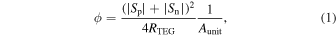
where Sp and Sn are the Seebeck coefficient of the p- and n-leg, RTEG is the electrical resistance including the p- and n-leg, contact holes, and metal wiring, and Aunit is the area of the unit structure of the TEG, respectively. The SPGC in the unileg-TEG is normalized by half of the unit cell given by Aunit = (2Lleg + 4Lpad)Wn, where Lleg, Lpad, Wn are the Si-legs lengths, Si-pads lengths, and the n-legs width, respectively. In the bileg-TEG, the SPGC is normalized only by half of the unit cell given by Aunit = (2Lleg + 4Lpad)(Wp + Wn). In both TEG, Lpad is set to 3.0 μm.
3. Results and discussion
The electrical resistance of the p-n pair in the bileg-TEG and n-n pair in the unileg-TEG is decreased by shortening Si-legs with Wn = 36 μm and Wp = 55 μm, as shown in Figs. 2(a) and 2(b). The electrical resistance of the p-n pair in the bileg-TEG increases by thinning the width of p-legs with Wn = 36 μm and Lleg = 1 μm, as shown in Fig. 2(c).
The electrical resistance of the p-n and n-n pair is analyzed with a simple lumped parameter circuit model, as shown in Fig. 3. Assuming the model structure depicted in Fig. 1, the electrical resistance of each element is given by R = ρL/(tW), where ρ is the electrical conductivity, L is the length, t is the thickness, and W is the width of each element, respectively.
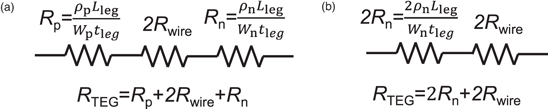
Fig. 3. (Color online) Simple lumped parameter circuit for (a) p-n pair of bileg-TEG and (b) n-n pair of unileg-TEG. The Rwire includes the resistance of the contact holes and metal wiring.
Download figure:
Standard image High-resolution imageWhen the Si-legs are shortened to less than 10 μm, the electrical resistance of the bileg-TEG obtained by the experiment and the FEM is larger than that obtained by lumped parameter circuit model. Contrary, the electrical resistances of the unileg-TEG obtained by the experiment, the FEM, and the circuit model are almost identical. The discrepancy between the experiment and the circuit model comes from the spreading resistance caused by carrier flow from the narrow n-leg to the wide p-leg, which was pointed out by a numerical simulation performed in the previous work. 19)
When the width of the p- and n-legs are aligned, the electrical resistances of the bileg-TEG obtained by the three methods are almost identical despite Lleg = 1 μm. By thinning or enlarging the width of the p-legs from 36 μm (=Wn), the experimental and FEM values of the electrical resistance become larger than the estimation with the lumped parameter circuit model.
Figures 4(a) and 4(b) show the distributions of the thermoelectric current, Jx , in p- and n-legs when Lleg = (a) 30 and (b) 1 μm, respectively. In the 30μm-long p-leg, the electric current is distributed over the full width of the leg, as shown in Fig. 4(a). Contrary, the current density in the 1 μm-long p-leg is non-uniform, and it is depleted in the area that protrudes from the width of the n-leg, as shown in Fig. 4(b). This non-uniform current flow is due to spreading resistance caused by carrier flow from the narrow n-leg to the wide p-leg. Since spreading resistance is inevitable in the miniaturized leg, increasing the width of the p-leg is not effective in enhancing SPGC, but rather just wastes the device area. Thus, it is better to reduce device area by aligning the widths of p- and n-legs to increase SPGC.

Fig. 4. (Color online) Distributions of thermoelectric current, Jx, in p- and n-legs when Lleg = (a) 30 and (b) 1 μm with Wn = 36 μm and Wp = 55 μm.
Download figure:
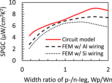
Standard image High-resolution imageTo optimize the ratio of the p- and n-leg width, the dependence of the SPGC on the ratio of the p- and n-leg width was evaluated, as shown in Fig. 5. In the circuit model shown as a red solid line, the optimal Wp/Wn ratio is obtained as 1.7, as numerically confirmed in previous work. 19) In the FEM calculation shown as a black dashed line, the optimal Wp/Wn ratio is obtained as approximately 1.6. When the material of wiring between Si-legs is changed from Al to Si, shown as a black dotted line, the optimal Wp/Wn ratio shifted to approximately 1.3. The effect of the spreading resistance appears when the electrical resistance of the wiring increases, as expected from Ref. 20. Thus, the performance of the miniaturized TEG is enhanced by not only aligning Wp/Wn but also decreasing the electrical resistance of wiring and other parasitic resistances.
Fig. 5. (Color online) SPGC of bileg-TEG v.s. width ratio of p- and n-leg. In FEM calculation, the material of wiring between Si-legs is changed from Al to Si, shown as dotted line.
Download figure:
Standard image High-resolution image
4. Conclusions
We investigated the dependencies of electrical resistance on the length and width of the Si-legs in the cavity-free planar bileg- and unileg-TEG. When using short Si-legs less than 10 μm, the electrical resistance of the bileg-TEG becomes larger than the simple estimation using the lumped parameter circuit model. This is due to the spreading resistance, which is caused when a current flows from a narrower leg to a wider leg. This effect is inevitable when the Si-leg is shortened to less than 10 μm. Although, the performance of the miniaturized TEG is enhanced by controlling the width ratio of the p- and n-legs and decreasing the parasitic electrical resistance. The width of the p- and n-legs in bileg-TEG should be carefully selected to maximize thermoelectric power concerning the spreading resistances of the legs.
Acknowledgments
This work was supported by the JST-CREST (JPMJCR15Q7, JPMJCR19Q5), by NIMS Nanofabrication Platform, and by AIST-SCR. We are grateful to Mr. Kawaguchi in Hamamatsu Photonics K. K. for offering stealth dicing.