
Abstract
A method to evaluate the interface trap density (Dit) accurately by using high-frequency C–V curves at InAs MOS interfaces is experimentally examined, where quick responses of the interface traps at room temperature make Dit evaluation based on the high-frequency C–V (Terman) method difficult. Therefore, low-temperature measurements of the C–V curves were performed to suppress the response of the interface traps. We studied the impact of the accuracy of the oxide capacitance COX, distribution function, and C–V hysteresis owing to slow traps on the Dit values evaluated by the Terman method. It was found that the accuracy of COX and the choice of distribution function had a slight effect on the accuracy of the Dit evaluation. It was also revealed that a measurement temperature lower than 40 K and limited gate voltage ranges in the C–V scan were indispensable for the accurate evaluation of Dit.
Export citation and abstract BibTeX RIS
1. Introduction
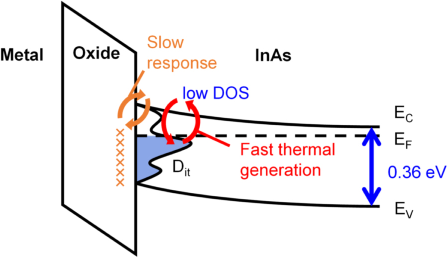
InAs has attracted considerable attention as a channel material for advanced MOSFETs with high-k gate insulators because of its superior electron transport properties. 1–7) InAs is also promising for photodiodes (PDs) in the near-infrared region because of its narrow band gap, superior avalanche multiplication gain, and low excess noise. 8–11) However, the InAs MOS channel has the problem of high interface trap density (Dit) at high-k/InAs interfaces, 12–19) which significantly degrades the performance of MOSFETs and PDs, such as reliability, drive current, dark current, and subthreshold swing. Therefore, a fabrication method to reduce the high Dit is required, indicating the importance of the accurate evaluation of Dit values. However, there are challenges in the accurate evaluation of Dit at InAs MOS interfaces, including many interface traps with a wide range of time constants, as shown in Fig. 1. First, there are many fast interface traps because the narrow band gap of 0.36 eV causes fast thermal generation and recombination of carriers between interface traps and bands. 12,13) Second, there are many slow traps, resulting in the large hysteresis of capacitance-voltage (C–V) measurements owing to border traps in the oxides. 12,13,16,18) The coexistence of considerable fast and slow traps makes it difficult to apply the conductance method to InAs MOS interfaces. 12) Therefore, the Terman method is suitable for the accurate evaluation of Dit, which is based on C–V curves under the high-frequency limit. The Terman method determines Dit by comparing the experimental C–V curve under the high-frequency limit and the theoretical ideal C–V curve without Dit. 20) However, guidelines on how to apply the Terman method to InAs MOS interfaces remain unclear. Thus, the measurement method used to obtain C–V curves under the high-frequency limit, and the calculation method of the ideal C–V curve should be clarified for InAs.

Fig. 1. (Colour Online) Schematic representation of an energy band diagram of an InAs MOS structure under the depletion condition; the fast response of interface traps by thermal generation and recombination and the slow response of slow traps.
Download figure:
Standard image High-resolution imageTherefore, in this study, the C–V curves were obtained under the high-frequency limit by performing measurements at low temperatures to slow down the thermal generation and recombination of the interface states. While it has been reported that the high-frequency limit cannot be obtained at 140–180 K, 12,13) there are still no detailed reports on the impact of measurement temperatures on C–V characteristics of InAs MOS capacitors, and the Dit evaluation using the Terman method. In this work, we examine the temperature at which the high-frequency limit can be obtained by systematically changing the measurement temperatures down to significantly lower temperatures of 31 K. Additionally, we have clarified that the response of slow traps can be suppressed by limiting the sweeping range of the gate voltage, resulting in the negligible impact of slow traps on the Dit evaluation.
Furthermore, we studied issues regarding the validity of the theoretical C–V curves: (1) the influence of the accuracy of the estimated oxide capacitance (COX), and (2) the choice of the Fermi–Dirac or Boltzmann distribution, which can be critical to the accurate evaluation of Dit at low temperatures using the high-frequency C–V method. For issue (1), the value of COX used to calculate the theoretical C–V curve can be determined by fitting the experimental C–V curve in the accumulation region. However, it is difficult to determine the semiconductor capacitance (Cs) of InAs in the accumulation region from experiments because of the high interface trap capacitance, as shown in Fig. 2. 15,21–24) The ideal Cs of InAs without Dit is considerably low because of the significantly low density of states (DOS), 2,24–26) while the real Cs of InAs can be significantly high owing to many interface traps. 21–24) The difference between ideal and real Cs makes it difficult to determine COX experimentally. Therefore, it is necessary to discuss the impact of the accuracy of COX estimation on Dit evaluated by the Terman method.
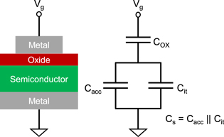
Fig. 2. (Colour Online) Equivalent capacitance model of an MOS capacitor under the accumulation condition. Cacc and Cit are the semiconductor and interface traps capacitance, respectively.
Download figure:
Standard image High-resolution imageFor issue (2), the Fermi level tends to be located inside the conduction band at low temperatures for InAs because of the considerably low DOS of electrons. 19,24) Therefore, the Boltzmann distribution should be inaccurate for simulating electron concentrations in the InAs band structure, while the Boltzmann distribution is used to simplify the calculation. Therefore, in this study, the impact of the choice of the distribution function on Dit evaluated by the Terman method was examined. In comparison with the published abstract, 27) new simulation results considering the quantum effect on the two-dimensional electron gas (2DEG) in the accumulation region and in-depth discussions on the accuracy of Dit evaluation have been added in this study.
2. Experimental methods
The process flow of the n-type InAs MOS capacitors is shown in Fig. 3. First, the unintentionally doped (100) InAs substrate was cleaned with acetone for 1 min, followed by BHF cleaning to remove the native oxide.
12) Thereafter, the (NH4)2Sy solution was used to passivate the InAs surface by sulfur atoms.
28) The soaking times of the substrates in the BHF and (NH4)2Sy solutions were 15 s and 5 min, respectively. The concentrations of BHF and (NH4)Sy in water were 22% and 0.6%–1%, respectively. The cleaning was performed at room temperature (R.T.). After each treatment, samples were rinsed with H2O. Subsequently, 120-cycle-Al2O3 (∼10 nm) deposition was performed at 200 °C by atomic layer deposition (ALD) using trimethylaluminum (TMA) as a precursor and H2O in the PicoSun ALD system.
29) The carrier gas was N2 at flow rates of 150 sccm and 200 sccm for TMA and H2O, respectively. The pulse times and purge times of them were 0.1 s and 4.0 s, respectively. The 120 nm thick Al gate electrode was fabricated by thermal evaporation. Finally, a 300 nm thick Al contact was deposited on the back side, followed by rapid thermal annealing at 350 °C for 1 min. The gate electrode was circular, with a diameter of 200 μm. The donor concentration ND of the InAs substrates was determined to be 1.84 × 1016 cm−3 by Hall measurements at room temperature. Here, the Hall scattering factor  of 1.1 is used because
  is limited by polar optical phonon scattering, which is dominant for InAs, and is known to be 1.1.
30,31) The C–V measurements were performed in a cryo-prober. The temperature was varied from room temperature to 30 K.
is limited by polar optical phonon scattering, which is dominant for InAs, and is known to be 1.1.
30,31) The C–V measurements were performed in a cryo-prober. The temperature was varied from room temperature to 30 K.
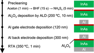
Fig. 3. (Colour Online) Process flow of InAs MOS capacitors and the schematic cross-sectional view.
Download figure:
Standard image High-resolution image3. Results and discussion
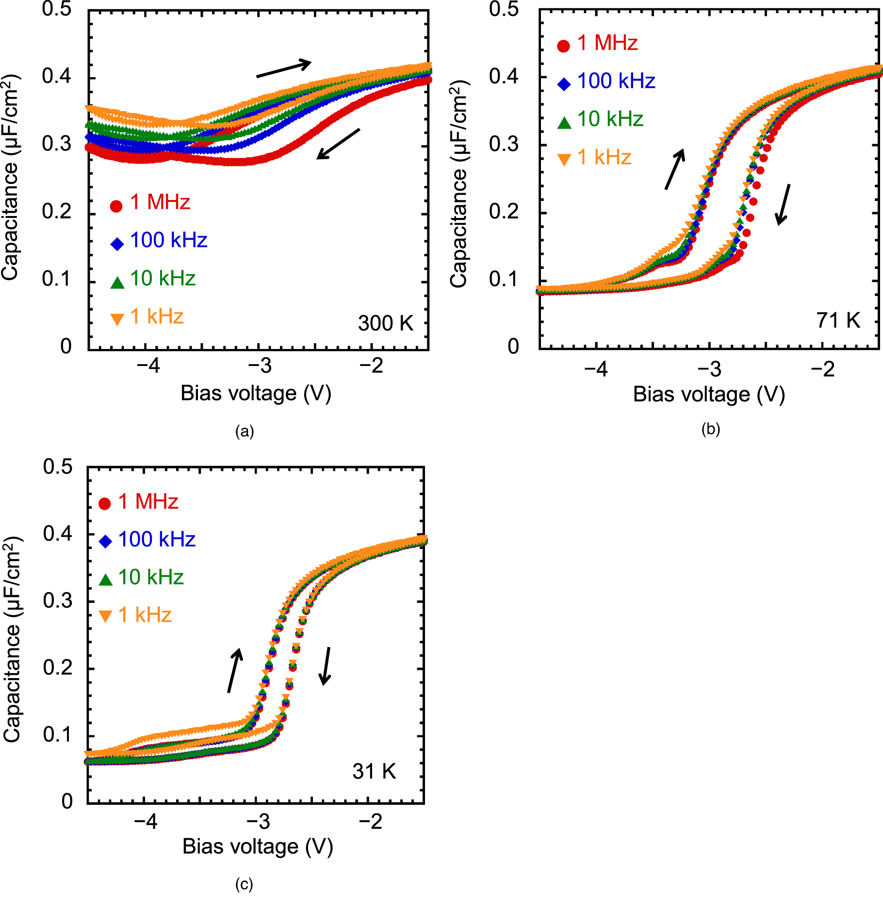
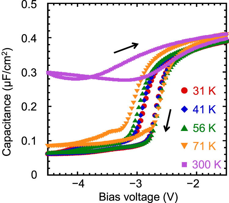
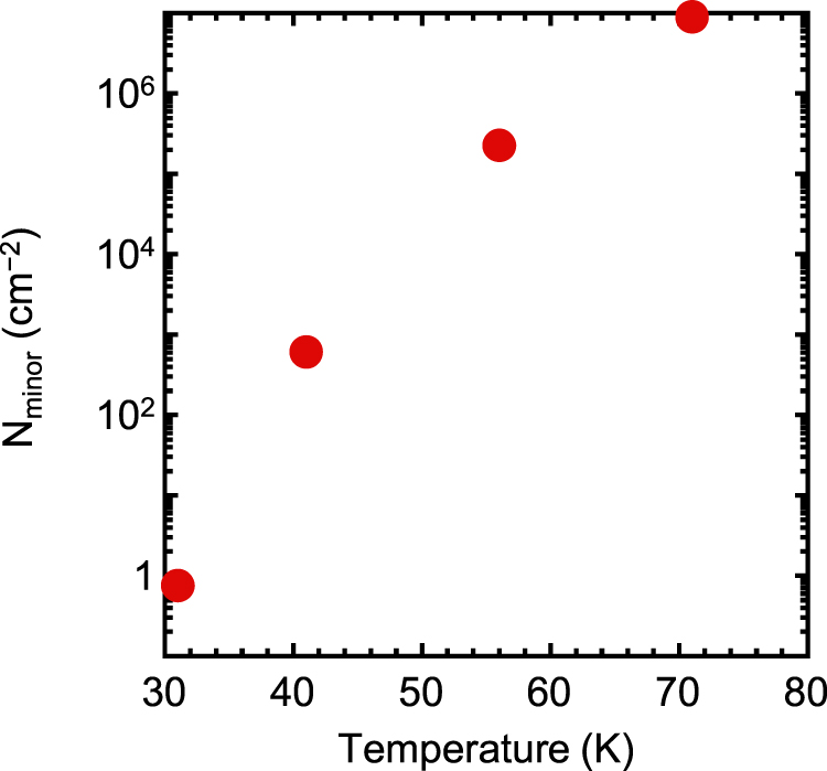
Figures 4(a)–4(c) show the C–V curves with bias voltages ranging from −1.5 to −4.5 V at 300 K, 79 K and 31 K, respectively, as a function of the measurement frequency from 1 MHz to 1 kHz. The capacitance change is less steep, and the frequency dispersion is larger at room temperature, which is attributed to the fast responses of the interface traps. However, the slope becomes steeper and the frequency dispersion decreases with decreasing temperature, which is attributed to the suppression of the high-frequency responses of interface traps at lower temperatures. Figure 5 shows the temperature dependence of C–V curves at 1 MHz. It was clearly confirmed that the slope became steeper with decreasing temperature. The C–V curves between 41 and 31 K were similar, suggesting that a high-frequency limit can be obtained in this temperature range. One of the concerns of C–V measurements at low temperatures is the freeze-out of the carriers. However, it is well known that for n-type InAs, the carriers do not freeze even at 4 K because the donor level is located above the conduction band edge. 32,33) Furthermore, this is confirmed in Fig. 4(c), where there is no measurement frequency dependence of the accumulation capacitance at 31 K, indicating that the increase in the substrate resistance component owing to freeze-out is negligible in the present measurements. Figure 6 shows the temperature dependence of the minority carrier density in an n-InAs MOS capacitor when −4.5 V is applied. Under this bias condition, the Fermi level was located within the band gap, approximately 0.06 eV upper above the edge of the valence band, even for a large negative applied voltage. Consequently, the minority carrier density was strongly dependent on the temperature. However, the values are smaller than the interface state density, indicating that the impact of minority carriers is negligible in the present analysis. Such a low areal density is owing to the Fermi-level position cannot reach the valence band edge at any temperature because of the large Dit in the MOS interfaces of In-based III–V semiconductors, which causes strong Fermi-level pinning near the valence band side of the band gap.
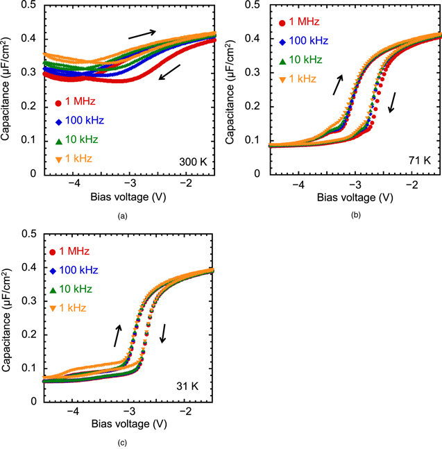
Fig. 4. (Colour Online) C–V characteristics of InAs MOS capacitors at (a) 300 K, (b) 71 K, and (c) 31 K.
Download figure:
Standard image High-resolution image
Fig. 5. (Colour Online) Temperature dependence of C–V characteristics of InAs MOS capacitors at 1 MHz.
Download figure:
Standard image High-resolution image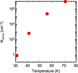
Fig. 6. (Colour Online) Temperature dependence of the areal density of minority carriers of InAs MOS capacitors when −4.5 V is applied. Under this bias condition, the Fermi level is located within the band gap, around 0.06 eV upper from the edge of the valence band, even for the large negative applied voltage.
Download figure:
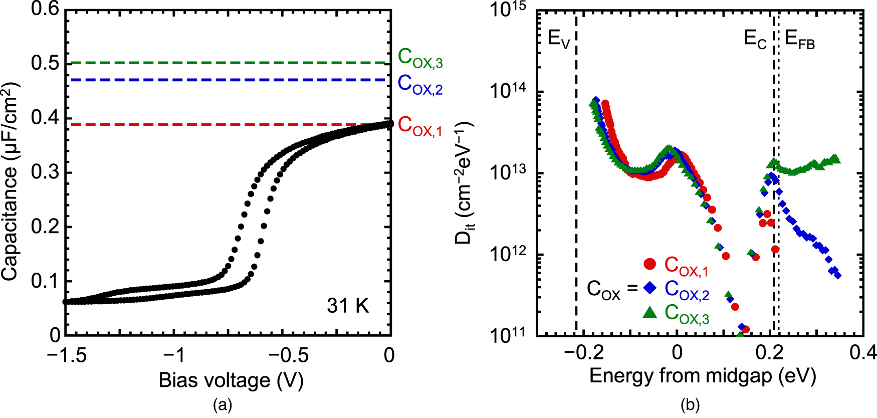
Standard image High-resolution imageTo evaluate Dit using the Terman method, it is necessary to confirm the validity of the conditions under which the theoretical C–V curve is calculated. First, we investigated the impact of the accuracy of the estimated COX on Dit evaluated by the Terman method. The oxide capacitance COX was experimentally determined by fitting the experimental C–V curves in the accumulation region. However, as shown in the equivalent capacitance model in Fig. 2, it is difficult to determine COX for InAs because Cit is an unknown value, and can be larger than the accumulation-layer capacitance (Cacc). 24) Note that the typical capacitance equivalent thickness (CET) of Cacc is ∼2 nm for InAs, which is five times thicker than that of Si. 24) To investigate the impact of COX, the three cases of COX are compared, as shown in Fig. 7(a).
- (1)COX = COX,1 for Cit = ∞, where COX,1 is the maximum value of the measured capacitance Cmax.
- (2)COX = COX,2 for Cit = 0 determined by fitting the experimental curve without considering the quantum confinement effect of 2DEG at the interface. 34) The electrons are modeled as three-dimensional carriers in the entire region, and the carrier density is calculated using the Fermi–Dirac distribution.
- (3)COX = COX,3 for Cit = 0, considering the quantum effect of 2DEG at the interface. Here, the wavefunction of the 2DEG and the potential were calculated by solving the Schrödinger and Poisson equations self-consistently. CET of Cacc is 2.0 nm for the 2DEG density Ns of 2 × 1012 cm−2, where the measured capacitance is Cmax at the bias voltage of −1.5 V.

Fig. 7. (a) Experimental C–V curve of the InAs MOS capacitor at 31 K and 1 MHz. The three different values of COX used in the simulation are also shown as COX,1, COX,2 and COX,3. (b) Energy distributions of Dit at the InAs MOS interface, evaluated by the Terman method using Fermi–Dirac distribution, under the assumption that COX is COX,1, COX,2 and COX,3. EFB is the flat band energy.
Download figure:
Standard image High-resolution imageSpecifically, COX,1 and COX,3 correspond to the minimum and maximum limits, respectively, of COX. Figure 7(b) shows the energy distributions of Dit evaluated using the Terman method for the C–V curves at 31 K using the Fermi–Dirac distribution under the assumption that COX is COX,1, COX,2, and COX,3. Note that the evaluated interface traps near the conduction band are not valid for the Terman method because the interface traps can quickly respond; thus, the response is included in the capacitance component because of the existence of many free electrons near the interface. Therefore, the Dit values near the conduction band, evaluated by the Terman method, are inaccurate, regardless of the COX we assumed. In addition, there are small shifts in the surface potential on the valence band side; however, these shifts are significantly small, even under a relatively large change in COX. Therefore, it is shown that this ambiguity in COX does not provide a meaningful error in Dit, as evaluated using the Terman method. Although it is a challenge to determine COX accurately from C–V curves because of the large Cit for III–V semiconductors with low electron effective mass, such as InAs, these results indicate that the accurate determination of COX is not a critical factor in Dit evaluation. Because InAs has a large Cit, COX,1 is closer to the true COX. Therefore, COX,1 was used for the subsequent calculations of the theoretical C–V curves.
Second, we investigated the impact of the choice of Boltzmann and Fermi–Dirac statistics in the calculation of the theoretical C–V curves on the Dit evaluation. Figure 8 shows the energy distributions of Dit evaluated by the Terman method using the Fermi–Dirac and Boltzmann distributions. There was almost no difference, except near the conduction band. As previously described, the Dit values near the conduction band, evaluated by the Terman method, were inaccurate, regardless of the assumed distribution type. Because there is no difference in Dit near the midgap, where the Terman method is valid and accurate, the choice of the distribution function has a slight effect on the evaluated Dit. This is because the Fermi energy is far from the conduction and valence band edges in the depletion region; thus, the Boltzmann statistics remain valid for the calculation of the capacitance under the depletion condition. However, the Fermi–Dirac distribution was used for subsequent calculations of the theoretical C–V curves, which provided highly accurate calculations at low temperatures.

Fig. 8. (Colour Online) Energy distributions of Dit at the InAs MOS interface at 31 K and 1 MHz by using the Fermi–Dirac distribution and the Boltzmann distribution in the calculation of the theoretical C–V curve under the assumption that COX is COX,1.
Download figure:
Standard image High-resolution imageFurthermore, the influence of the C–V hysteresis owing to slow traps should be examined. Figure 9(a) shows the hysteresis of C–V curves for two different voltage scan ranges. When the voltage range is wide from −1.5 to −4.5 V, the observed hysteresis causes the difference in the slope of the capacitance change between the forward and backward sweep. As shown in Fig. 9(b), slow traps have a significant impact on the evaluated Dit. Especially in the forward sweep, the de-trapping of holes from slow traps or trapping of electrons into slow traps makes the slope less steep, resulting in a higher apparent Dit. However, as shown in Fig. 9(a), the hysteresis can be eliminated, and the C–V curves between the forward and backward sweeps become identical by utilizing the narrow voltage scan range from −2.4 to −2.9 V. Consequently, the evaluated Dit is almost the same between the forward and backward sweeps, as shown in Fig. 9(b). It is also shown that the slow traps are mainly charged when a negative gate bias voltage is applied because the C–V curves of the backward sweep are almost the same for the wide and narrow voltage ranges. This is surprisingly different from the general behavior of slow traps, such as Ge MOS interfaces. 35) Slow traps are charged in the accumulation region because slow traps originating from the border traps inside the gate insulators and free carriers at the interfaces are required to charge the border traps. However, the slow traps of InAs MOS interfaces are charged only in the depletion region, although theoretical calculations suggest that no inversion carriers are generated, and there are no free carriers at the interface. The origin of slow traps at InAs MOS interfaces remains unclear. The important points in the C–V measurement are the careful selection of the minimum value of the negative gate bias to suppress the trapping/de-trapping of charges in slow traps and to use C–V curves measured in a narrow voltage range for the Terman method.
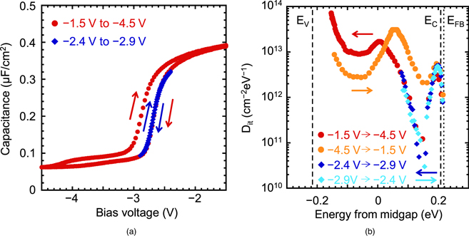
Fig. 9. (Colour Online) (a) Hysteresis of C–V curves of InAs MOS capacitors at 31 K for 1 MHz in the bias voltage ranges of −1.5 to −4.5 V and −2.4 to −2.9 V. (b) Energy distributions of Dit at the InAs MOS interface, evaluated by the Terman method using the C–V curves of the forward and backward sweep with the narrow and wide voltage ranges using the Fermi–Dirac distribution under the assumption that COX is COX,1.
Download figure:
Standard image High-resolution imageFinally, Fig. 10(a) shows the temperature dependence of the C–V curves in a narrow voltage range with negligible hysteresis. Similar to Fig. 4, the C–V curves between 40 and 31 K were almost identical, indicating that the high-frequency limit was obtained. Figure 10(b) shows the energy distributions of Dit evaluated from the C–V curves using the Terman method. EC and EFB were used at 31 K. Note that the changes in EC and EFB owing to temperature changes are considerable small, and have a slight impact on the plot of the Dit distributions at different temperatures. Because the Dit values are almost similar between 40 and 31 K, it can be judged that an accurate evaluation of Dit at the InAs MOS interfaces was achieved by the Terman method using the proper conditions clarified in this study. Consequently, a minimum value of Dit of ∼1011 cm−2 eV−1 was obtained for the ALD Al2O3/InAs MOS capacitors.

Fig. 10. (Colour Online) (a) Temperature dependence of C–V curves of the InAs MOS capacitor at 1 MHz in the bias voltage range of −2.4 to −2.9 V. (b) Temperature dependence of the energy distributions of Dit at the InAs MOS interface evaluated by the Terman method using the Fermi–Dirac distribution under the assumption that COX is COX,1.
Download figure:
Standard image High-resolution image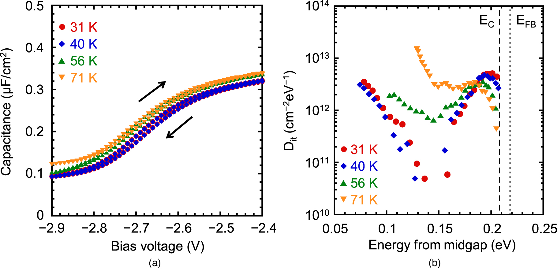
4. Conclusions
We studied the influence of the measurement conditions of C–V characteristics and the theoretical model in the calculation of the ideal C–V curves on the Dit evaluation at the InAs MOS interfaces using the Terman method. Consequently, the C–V measurements at less than 40 K are necessary to suppress the response of interface traps, and to obtain the high-frequency limit of the C–V curves. A small negative gate voltage should be chosen to suppress the hysteresis of C–V curves because slow traps are charged in the surface potential near the valence band. In the calculation of the ideal C–V curves, the choice of the Fermi–Dirac or Boltzmann statics and the accuracy of COX, which cannot be simply obtained from experimental C–V curves on III–V semiconductors, have a slight impact on the Dit evaluation. These guidelines allow us to evaluate Dit accurately using the Terman method. Consequently, the Dit of the ALD-Al2O3/InAs interface was accurately evaluated, and the minimum value of Dit was ∼1011 cm−2 eV−1.
Acknowledgments
This work was supported by JSPS KAKENHI, Grant Nos. 22H00208 and 21J10272, Japan, and by a project, JPNP16007, commissioned by the New Energy and Industrial Technology Development Organization (NEDO), Japan.