

Abstract
We propose an efficient array measurement test structure to measure many devices and to obtain statistical characteristics of organic thin-film-transistors (OTFT) for long-term reliability evaluation of new devices under development in laboratories and those that cannot achieve sufficient yield. We propose to adopt different devices from the device under test for the array control circuit. We implemented a separate control circuit as a dedicated relay-switch board without device consolidation. This relay-switch board can also apply voltage stress to any number of devices under test for negative bias temperature instability evaluation. The interface issue between the chip and board is resolved with a flexible flat cable and an anisotropic conductive film. The proposed measurement system successfully measured the OTFT arrays in (sweep time of source measure unit) × (number of OTFTs) period, and only requires 84 min for 64 nOTFTs (n-type OTFT) (552 points/device), which corresponds to 1.3 min/device in the experiment.
Export citation and abstract BibTeX RIS
1. Introduction
Flexible or printable organic devices are considered the prospective devices in the coming Internet of Things (IoT) era, and implementation of thousand-gate scale logic circuits brings more complex functions related to communication, peripheral circuits to sensors, 1) or other IoT devices. For example, the implementation of organic thin-film transistor (OTFT) circuits 2) and their applications have recently been reported, e.g., transponder chips for radio frequency identification (RFID) tags; 3,4) static random-access memories (SRAMs); 5) CMOS analog circuits such as amplifiers, analog-to-digital (A/D), and digital-to-analog (D/A) converters; 6,7) CMOS digital circuits such as microprocessors; 8) artificial skin using thermal and pressure sensors; 9) braille displays using SRAM; 10) and wearable electrochemical sensors. 1)
One drawback of OTFTs is that the carrier mobility in organic semiconductors is lower than that of silicon and as a result, extensive studies have been performed to improve carrier mobility in organic semiconductors. 11–19) In recent studies, a hole mobility of 30 cm2 V s−117) and an electron mobility of 3 cm2 V s−116) were achieved. An additional concern for early OTFT works was that the operation voltages of the OTFTs were a few tens of volts and consumed a large amount of power, thus lowering the operating voltage of the logic circuits composed of OTFTs is a focus of recent research. Considerable effort has been expended on low-voltage operations of OTFT logic gates in the range of 5 V to 15 V. 20–23) Our past work included the low-voltage as a security component 24,25) with a 3.3 V operation and low-leakage current logic gates 26,27) with a 2.5 V operation.
Long-term reliability, that is, time degradation issue, is also one of the important challenges concerning OTFTs because OTFTs degrade in a few months in ambient air. 28,29) However, research on the evaluation of long-term reliability with the measurement of many transistors is seldom found. While there have been several studies on OTFT arrays with 25 OTFTs, 30) 50 OTFTs, 31,32) 110 OTFTs, 33) 200 OTFTs, 34) presenting statistical characteristics, these works do not assess long-term reliability. In the work on the evaluation of long-term reliability, 35,36) few devices were evaluated for the long term, and statistical characteristics of time degradation were not presented.
Long-term testing is needed, but to obtain current–voltage (I–V) characteristics of many OTFTs using a manual prober, one must spend several or more days measuring. In addition, the metal electrodes made of thin-film are not suitable for repetitive probing. It can be broken after a few tens to hundreds of uses. Repetitive measurement over several months for the evaluation of long-term reliability with manual probing is impractical. Evaluation of a larger number of OTFTs or longer-term reliability evaluation requires more efficient measurement methods.
This study focuses on the implementation of the test structure for the long-term reliability evaluation of new devices, and presents an efficient measurement method of many OTFTs based on array measurement methods for silicon transistors. The prototype of the measurement method is presented in our previous paper. 37) This study proposes an efficient long-term reliability evaluation method for new devices and measures 64 OTFTs in an experiment. The evaluation of hundreds, thousands, or more devices using our improved method can be considered the novelty of this study. The contributions of this work are summarized below
- Anticipating transistor array measurement with a device under the test (DUT) selection circuit composed of the different devices from DUT.
- Introduction of the array measurement system requiring reasonable human resource, fabrication, and instrument costs for the long-term reliability measurement of new devices which are under development in the laboratory and cannot achieve a sufficient yield or on-off ratio.
- Implementation of the low-leakage DUT selection circuit board as a practical solution for selecting a circuit comprising an interface between the organic device test chip and the printed circuit board.
- Achievement of the automated transistor array measurement for 64 OTFTs.
Based on that previous work, herein we propose a measurement method using an external relay-switch printed circuit board (PCB) to select the DUT transistor, and designed the dedicated relay-switch board for measurement. We also present the test element group (TEG) structures for array measurement that suits external relay-switch boards. The efficient array measurement using the designed relay-switch board, TEG structure, and statistical OTFT characteristics calculated from experimental data, are demonstrated.
2. The measurement method using the external relay-switch board
This section explains the proposal and development of an array measurement method using external relay-switch boards for the long-term reliability evaluation of new devices under development in laboratories. Section 2.1 describes the concept of proposing an array measurement method for new devices, and highlights its novelty compared with the conventional array measurement method used for silicon transistors. Section 2.2 explains the structure of the external relay-switch board for the proposed method. We have also mentioned in detail the relay elements adopted for implementing the relay-switch board in Sect. 2.3. Section 2.4 describes the design of the OTFT TEG for the proposed method and Sect. 2.5 explains the measurement procedure using the proposed relay-switch board. Section 2.6 compares the proposed and conventional measurement methods using an auto-prober based on the implementation of our method described in Sects. 2.2–2.5.
2.1. Array measurement method for the long-term reliability evaluation of new devices under development in laboratories
As described in the Sect. 1, several previous studies exist on the array measurement of silicon transistors 38,39) for the measurement of many transistors. Figure 1 shows the fundamental structure of the array measurement. These methods implement on-chip select circuitry which uses the same device as the DUT for a measurement control circuit and are based on high yields of silicon transistors.

Fig. 1. Example of conventional array measurement circuits of silicon transistors. 38)
Download figure:
Standard image High-resolution imageConversely, it is challenging to implement the control circuit of array measurement using new devices as long as they cannot achieve a sufficient yield or on-off ratio. When different devices, which can achieve sufficient yield or performance, can be consolidated in the measurement target new device, the array control circuit for such devices can be implemented. However, new devices are frequently fabricated on a non-silicon substrate, and thus, reliable silicon transistors cannot be adopted. In addition, the consolidation of different devices on the same chip is challenging. Adopting different reliable transistors for an array control circuit is difficult for most new devices.
In this study, we introduced the separation of the DUT chip and control circuit and implemented the array control circuit on the external circuit board. A DUT chip and array control circuit were fabricated separately, and the fabrication was not challenging. The connection between the DUT chip and control circuit board can be an implementation issue, and we describe the connection method in the Sect. 2.2.
2.2. Structure of the proposed array measurement system using the relay-switch board
Herein, we describe a measurement system using an external relay-switch board. An OTFT array TEG is implemented on the OTFT chip, and an OTFT on the TEG is selected by the external board. The new devices generally do not have the method to connect with the circuit board. In this paper, we adopt attaching a flexible flat cable (FFC) to the OTFT test chip with an anisotropic conductive film (ACF). 24) FFC is attached to pads on an OTFT chip with ACF by applying heat and pressure while ensuring conductivity. This method implements the commonly used FFC on the test chip of new devices and realizes the compatibility with the common circuit board implementations. Once the FFC is connected to the board, the connection is secured during the long-term evaluation of many transistors. The proposed measurement method does not need to consider the degradation issue of metal electrodes by repetitive probing. The external board can be controlled electrically, and thus the measurement of all OTFTs on the TEG requiring manual operation can be automated.
Figure 2 shows the circuit structure of the external relay-switch board, and Fig. 3 is an image of the fabricated board. The size of the fabricated board is 226.0 mm × 185.9 mm. The implemented board has six Bayonet Neill Concelman (BNC) ports for the source measure unit (SMU) and an 80-bit bus for connection to an OTFT chip. Here, six ports are named SMU1-6, and SMU1 and SMU2 can be connected to any of the 64-bit of the 80-bit bus to the OTFT chip, and SMU3-6 are each directly connected to 4-bit in the 80-bit bus respectively. The 64-bit is selected by the relays in the following manner. Two relays are allocated for each of the 64-bit interface ports to the chip, and one of two relays for each interface port switches the connection to SMU1 or high impedance. Another switches the connection to SMU2 or high impedance. Thus, each 64-bit port has three states, connected to SMU1, connected to SMU2, and high impedance. This three-state configuration assumes setting the port to high impedance, grounded, or voltage applied. Relays are controlled by the set and reset signals. These two signals determine the set or reset state. In this board, the set state of the relay corresponds to the connection to the SMU, and the reset state corresponds to the high impedance. When both relays for a certain port to the chip are in the reset state, the port is set to high impedance. When one of two relays is in the set state and another is in the reset state, the relay is connected to SMU1 or SMU2. Setting both relays to the set state is exclusive. Relay and reset signals are supplied via analog multiplexers. By inputting the address to the analog multiplexers, the relay where set or reset is input is controlled. As there are two relays (connecting SMU1, and SMU2) for each OTFT on the TEG, these relays are identified by the different relay addresses. Therefore this board has 64 ports to chip, 128 relays, and 128 relay addresses.

Fig. 2. Circuit structure of the relay-switch board.
Download figure:
Standard image High-resolution image
Fig. 3. (Color online) Image of manufactured measurement board.
Download figure:
Standard image High-resolution imageThe relay-switch board is fabricated as the four-layer substrate with a through-hole. Interstitial via hole or the build-up method is not required, and the fabrication cost of the substrate is reasonable. The board is designed in KiCAD, which is free software for PCB design and is applicable for commercial board design, and the electronic design automation software is free.
2.3. Relay element for selecting DUT and its impact on long-term measurement
The relay element is suitable for observing the leakage current of the OTFT since it mechanically opens the connection. Therefore the leakage current of the transistors, other than the selected DUT, can be reduced compared with that of MOSFETs, achieving high accuracy in the off-leakage current measurement. The latching relay (OMRON G6KU-2F-Y 5.0V) is adopted for the relay elements.
Latching relays keep their state after the relay is set or reset though a non-latching relay requires the application of the set voltage and current to keep the state. The states of the latching relays are controlled by the set and reset signals of the relays, and after the set or reset signal is input to the relay, its state is held until the next set or reset signal is applied. In the measurement of the impact of voltage stress, voltage is applied to the DUT for several days or weeks, thus the latching relays are adequate for long-term measurements. In addition, this design with the latching relay can connect the multiple terminals of DUT with SMU, and can apply the voltage stress to multiple DUT elements. This feature is effective for negative bias temperature instability (NBTI) evaluation. 40–43)
2.4. OTFT TEG design and gate short fault issue
In our previous work, 37) our measurement system suffered from a gate short fault issue. Figure 4 shows the one-dimensional OTFT array TEG of the previous work. In this TEG design, all OTFTs share a gate and a source terminal, and drain terminals are selected by the external board. However, when the gate short fault occurs at any OTFT, the gate voltages of other OTFTs also cannot be applied because of the short current path from the gate to the source, and all OTFTs on the TEG cannot be measured [Fig. 5]. In previous work, we disconnected defective OTFTs by cutting their source terminals using a manual prober as a solution. However, additional gate short failure can occur during the long-term reliability measurement. Manual wire cutting every time an additional gate failure occurs is inefficient and can be an obstacle to collecting OTFT characteristics in the long term.
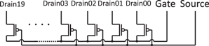
Fig. 4. TEG structure of a one-dimensional array in the previous work. 37)
Download figure:
Standard image High-resolution image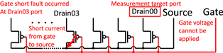
Fig. 5. (Color online) Gate short defect issue of TEG in previous work. When a short defect occurs at any OTFT, the gate voltage cannot be applied because the source terminal is shared and there is a shorted current path from the gate to the source.
Download figure:
Standard image High-resolution imageIn this work, we improved the TEG structure as shown in Fig. 6. In this TEG, two external boards are used for the measurement. The drain terminals are selected by one external board, and the source terminals are selected by the other board respectively. The drain and source terminals of the target OTFT are connected to the SMU and the drain and source terminals of other OTFTs are set to high impedance. In this configuration, the gate short defect at non-measurement target OTFT does not have a shorted current path to drain or source [Fig. 7]. As short current is prevented, the gate voltage of measurement target OTFT can be applied, and cutting the source terminal of the defective OTFT is unnecessary.

Fig. 6. TEG structure of a one-dimensional array in this work.
Download figure:
Standard image High-resolution image
Fig. 7. (Color online) The gate short defect can be prevented in the improved array TEG. The gate short defect at non-measurement target OTFT does not affect the measurement target OTFT because the source terminals are not shared and have high impedance.
Download figure:
Standard image High-resolution image2.5. Automated measurement procedure
The measurement procedure using the external relay-switch board and OTFT TEG can be automated. There are two manual operations: the measurement instruments setup, attaching the FFCs of OTFT TEG chip drain and source terminals to two boards. After this preparation, the automated measurement procedure can be started.
The automated measurement procedure repeats three steps; selecting the target OTFT to SMU by controlling the relays, sweeping bias voltages by the SMU, and disconnecting the target OTFT from the SMU. When selecting the target OTFT, a relay set signal is asserted after the relay address is input that connects the target OTFT and SMU1. These procedures are done for two boards that correspond to the drain and source terminals. Measuring by the SMU can be done with the SMU sweep function. After measurement, disconnecting the target OTFT from the SMU is accomplished by inputting the relay address and asserting a relay reset signal. The input address and the set and reset signal of the relay can be automated by the pattern generator. This measurement procedure can be automatically done for all OTFTs on the TEG by controlling the SMU and the pattern generator with the computer,
2.6. Comparison with the conventional auto-prober
An auto-prober can also measure several transistors, and this section compares the proposed test structure with an auto-prober.
The proposed test structure using relay-switch boards has an advantage with respect to the suitability for long-term reliability evaluation to the measurement method using an auto-prober. The cost of instruments and required space for the measurement environment are also reasonable in our proposed method.
An auto-prober can automatically change the contact position, and can automatically measure all the DUTs on a chip. However, a flexible substrate is easily worn, the contact time of DUTs on flexible substrates is limited, and it is challenging to contact the probe needles on the same DUT many times. The number of contact times is limited to approximately 10, This is a critical limitation for long-term reliability evaluation. The proposed method can automatically measure the 64 DUTs without changing the contact position to a DUT chip. The proposed test structure with the relay-switch board can electrically switch the measurement target DUT among 64 DUTs and can obtain detailed performance changes hour by hour. The durability of relay switching limits the switching of the DUT and is over 100,000 times. The applying voltage for DUTs is required for NBTI evaluation, which is one of the important degradation factors of transistors. However, an auto-prober cannot apply voltage to all DUTs. Any number of switches on the board can be set on or off, and the proposed test structure can apply the voltage to all DUTs for NBTI evaluation. As the auto-prober has a critical limitation concerning the number of the DUT and measurement frequency, the proposed test structure with the relay-switch board is considerably more suitable for long-term reliability measurements, including NBTI evaluation, than the auto-prober.
The proposed method can be implemented with the reasonable cost of the instruments and the required space for the experiments. The preparation cost of the board is the board fabrication cost. The test board does not require an expensive board fabrication configuration, and four boards can be fabricated for approximately $2000. On the other hand, an auto-prober itself costs over $100,000. Assuming that an SMU, which is required for all configurations, costs $20,000, the measurement environment of the proposed test structure costs at least less than 1/5th of a conventional auto-prober. The measurement environment of the proposed method, which includes an SMU, DUT, two relay-switch boards, the power supply of the board, and a pattern generator, can be set up on the table and be contained on a shelf when it is not used. Conversely, an auto-prober occupies one Sect. of the room. The proposed test structure notably decreases the cost and space required for preparing the measurement environment and facilitates long-term reliability evaluation in new devices.
3. Test chip
Figure 8 shows the image of the fabricated test element group (TEG) chip. The chip size is 2 cm × 5 cm. This chip is manufactured as a 5 cm × 5 cm size chip and cut with a glass cutter. Two FFCs are attached to the chip with an ACF as the board interfaces.
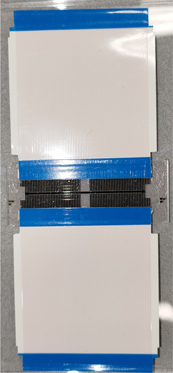
Fig. 8. (Color online) Image of the test chip. Two FFCs are attached to the chip. The chip size is 2 cm × 5 cm.
Download figure:
Standard image High-resolution imageFigure 9 shows the nOTFT structure implemented in this study. The semiconductor material of n-type OTFT (nOTFT) is TU-1. 44) This device 45) consists of an Al bottom gate electrode layer (gate), an AlOx insulator layer, a self-assembled monolayer (SAM), an organic semiconductor, and an Au top source or drain electrode. As the AlOx and SAM layers are sufficiently thin (4 nm and 2 nm thickness, respectively), devices operate at 3 V or lower, 27) which is the nominal operation voltage on printed carbon boards (PCB) or integrated circuit chips. Although we fabricated TFT devices in this paper with thermal deposition, the fabrication process can be replaced with printing technologies in the future as materials are developed and after considering compatibility with printing technologies.

Fig. 9. (Color online) Structure of an nOTFT in this paper.
Download figure:
Standard image High-resolution image4. Array measurement result with the proposed method
4.1. Measurement environment
Figure 10 depicts the connections of the measurement instruments, the proposed external board, and the OTFT test chip. Figure 11 summarizes the measurement procedures of the conventional manual probing method and the presented method. Figure 12 shows an image of the difference between measurement systems for a one-dimensional transistor array. Our measurement environment consists of the following components:
- the test chip with FFC
- external relay-switch board
- Keysight B2912A SMU
- Keysight M9187A Digital I/O
- Keysight U2722A SMU
- a computer for controlling the measurement instruments

Fig. 10. Overview of the measurement environment. Two external boards are connected to DUT with the FFCs. B2912A SMU supplies the drain, source (ground), and gate voltages to two boards. B9187A digital I/O instrument generates set and reset signals and relay address. PC controls B2912A SMU and B9187A digital I/O instruments and automatically operates the selection of transistors and voltage sweep measurements.
Download figure:
Standard image High-resolution image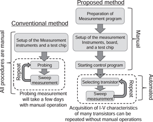
Fig. 11. Measurement procedure of conventional probing measurement (left) and of presented measurement method (right). Selection of transistors and sweep measurements, which require manual operations in the conventional method, are automatically operated in the presented method.
Download figure:
Standard image High-resolution image
Fig. 12. (Color online) The proposed boards and the test chip are connected for the measurement.
Download figure:
Standard image High-resolution imageThe test chip and two external relay-switch boards are connected to the FFC. The B2912A SMU has 10fA precision and is used to supply the drain, source, and gate voltages and obtain I–V characteristics. The B2912A SMU is connected to the proposed board with triaxial cables and triaxial-BNC conversion adapters. The B2912A SMU has two channels. Gate and drain voltages are supplied from these two channels, and source terminals are connected to the ground of the two channels. The digital output of M9187A is used for the relay address and the set and reset signals of the relays. The power supply and ground levels of the buffer and multiplexer ICs for the relay control on the relay-switch board and the control signal generated from M9187A are supplied by U2722A SMU. B2912A SMU, M9187A Digital I/O, and U2722A SMU are controlled by the computer. These instruments are all compatible with the API library for C# programming language development environment provided by the vendor of the instruments. We wrote the automated measurement program that automatically runs the measurement procedures: input the relay address (M9187A), input the relay set signal (M9187A), sweep measurement (B2912A) and input the relay reset signal (M9187A) for all 64 OTFTs of the TEG on the test chip. The power supply of the relay control (U2722A) on the board is supplied throughout the measurement. After the instruments are set up, the relay control power supply (U2722A) is turned on and the measurement program is started and no further involvement of the operator is needed for the experiment. As most of the measurement procedure is electrically controlled and automated, this array measurement method can significantly reduce the manual operation required for the measurement of many OTFTs.
4.2. I–V characteristics and measurement time
Figures 13 and 14 show the I–V characteristics of the 64 nOTFTs on the OTFT TEG obtained from the presented measurement system. In Fig. 13, the drain–source voltage (Vds) was swept from 0.0 V to 2.5 V (251 points) at a gate–source voltage (Vgs) = 2.5 V condition, and the drain–source current (Ids) was observed. In Fig. 14, Vgs was swept from −0.5 V to 2.5 V (301 points) at Vds = 2.5 V condition, and Ids was observed. The measurement of the I–V characteristics of 64 OTFTs in these two conditions finished in 84 min. The procedures during these 84 min are automated, and no manual operations were required. 36 OTFTs among 64 OTFTs showed the transistor operation. The gate short fault was observed in 14 OTFTs for the remaining 28 OTFTs, and gate-controlled switching operation as a transistor was not observed among the other 14 OTFTs.

Fig. 13. (Color online) Measured Ids–Vds characteristics (Vgs = 2.5 V) for 64 nOTFTs.
Download figure:
Standard image High-resolution image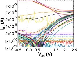
Fig. 14. (Color online) Measured Ids–Vgs characteristics (Vds = 2.5 V) for 64 nOTFTs.
Download figure:
Standard image High-resolution image4.3. Statistical characteristics
Figures 15–17 show the histograms of Ids, threshold voltage (Vth), and mobility (μ). Vth was calculated with the extrapolation method, and μ was calculated using the formulation of the saturation current of the transistor. The averages and standard deviations of Ids, Vth, and μ for the operated OTFTs were 0.364 μA and 0.145 μA, 1.85 V and 0.0727 V, and 0.155 cm2 V s−1 and 0.0479 cm2 V s−1, respectively. The normal distributions of the calculated average and standard deviation are also depicted in Figs. 15–17.

Fig. 15. (Color online) Distribution of Ids obtained by the described measurement method. Average and standard deviation of Ids are 0.364 μA and 0.145 μA respectively. OTFTs that were not operated were excluded.
Download figure:
Standard image High-resolution image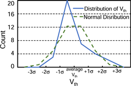
Fig. 16. (Color online) Distribution of Vth obtained by the described measurement method. Average and standard deviation of Vth are 1.85 V and 0.0727 V, respectively. OTFTs that were not operated were excluded.
Download figure:
Standard image High-resolution image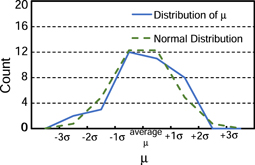
Fig. 17. (Color online) Distribution of μ (mobility) obtained by the described measurement method. Average and standard deviation of μ are 0.155 cm2 V s−1 and 0.0479 cm2 V s−1 respectively. OTFTs that were not operated were excluded.
Download figure:
Standard image High-resolution image
4.4. Discussion
The described measurement method successfully obtained the I–V characteristics of 64 OTFTs in 84 min, during which manual operations are not required. The measurement of 64 OTFTs with manual probing can take a few days, and manual operation is continuously required during the measurement with manual probing. The presented measurement method is much more efficient compared with the conventional manual probing method.
In the long-term reliability evaluation with this measurement method, after an initial setup of the instruments and preparation of the measurement program, the measurement of the I–V characteristics for many OTFTs can be automatically operated for several months. This automated measurement method considerably reduces the amount of manual operation required for long-term reliability testing and therefore, makes long-term reliability evaluations feasible.
In Figs. 13–14, the I–V characteristics of 64 OTFTs, measured with this method, are shown. The precision of the off-leakage currents of the OTFT was 1 × 10⁻¹¹ and is sufficient for the observation of the off-leakage current of the OTFTs.
As described in Sect. 4.2, there were 14 OTFTs with the gate short defect, and on/off operations were not observed in the 14 OTFTs among the 64 OTFTs on the TEG. Importantly, this measurement method could measure the OTFT characteristics without interference from the failed OTFTs because of the measurement configuration with two external boards and the described TEG structure. In addition, the proposed measurement method selects the measured transistor with the relays on the external board through the same device as the DUT selects the target device in the conventional array measurement method. This method could be applied to transistors that are in development and cannot be manufactured with high yield or sufficient performance.
In Figs. 15–17, the histograms of the Ids and μ calculated from the measured characteristics are close to the normal distribution. In the histogram of Vth, although the OTFT count in the −σ to average Vth range is high (20), the OTFT count in the −σ to σ range (27) is close to that of the normal distribution (24.6). This demonstrates that useful statistical data could be obtained with the automated method.
5. Conclusion and future work
This paper proposed an array measurement method using an external board for long-term reliability evaluation of OTFTs. Array measurement of the new devices which are under development in the laboratories and cannot achieve sufficient yield or on-off ratio is implemented with the relay-switch circuit board, an FFC interface between a chip and a board, and the OTFT array TEG on a chip. Our relay-switch board can apply voltage stress to more than one device and can be used for the evaluation of the NBTI of OTFTs. In the measurement of the I–V characteristics with the proposed measurement method, observing off- and on-currents of the OTFTs and avoiding interference from the defective transistors were successfully demonstrated. Measuring the I–V characteristics for 64 OTFTs on the TEGs was completed in 84 min. The measurement procedure for OTFTs on TEG was successfully automated using the measurement method with the relay-switch board. The measurement method notably reduced measurement time and manual operation compared with conventional manual probing measurement and makes long-term reliability feasible. Because the external board selects the measuring device, our method can also be applied to transistors that are under development and cannot achieve a high yield or high on-off ratio. Although we measured 64 devices in this study, the evaluation of the long-term reliability of a greater number of devices is expected for integrated circuit implementation. We will work toward the improvement of the proposed method to hundreds or thousands of devices as extensive future work.
Acknowledgments
This work was supported by the 2019 research grant program of the KDDI foundation. This work was partly supported by JSPS KAKENHI Grant No. 20H04156. This work was also supported by JSPS KAKENHI Grant No. 22K11966.