
Abstract
Zirconium disulfide (ZrS2)—an attractive next-generation channel material because of its high mobility—is stabilized in the air by a zirconium dioxide (ZrO2) film which functions as a high-k film in MISFET. We fabricated high-k/PVD-ZrS2 stacks with a self-oxidized ZrO2 film as an interfacial layer; their chemical properties were analyzed to clarify how each fabrication process affects the ZrS2 under the oxide film. The results clarified that sulfur vapor annealing (SVA) is critical for fabricating high-quality physical vapor deposition (PVD) ZrS2 films and that the change in surface potential of the ZrS2 films due to interface dipoles between the high-k and Zr-compound films is suppressed with scaling of high-k thickness. The SVA with high-k films also prevents degradation of crystallinity and stoichiometry, enhancing the quality of the ZrS2 films without affecting their surface potential. These achievements enable us to control the threshold voltage in ZrS2 MISFETs.
Export citation and abstract BibTeX RIS

Content from this work may be used under the terms of the Creative Commons Attribution 4.0 license. Any further distribution of this work must maintain attribution to the author(s) and the title of the work, journal citation and DOI.
1. Introduction
The improvements in transistor performance are sufficiently important for our lives that we have solved problems by various methods whenever we have faced them. 1) However, silicon (Si), which has been used as a channel material for several decades, faces the problem of a dramatically degraded mobility when scaled to the atomic-layer level, 2) thus necessitating the development of an alternative channel material to Si. Therefore transition-metal dichalcogenides (TMDCs) are attracting attention and are expected to be used in practical applications in the future. 3) The TMDCs have a layered structure, which not only prevents mobility degradation at the atomically thin scale but also theoretically enables a uniform and dangling-bond-free interface. 4)
Among the various TMDCs, zirconium disulfide (ZrS2), which has a 1T structure and an appropriate bandgap as a semiconductor, has attracted particular interest. 5) At the atomically thin scale, it theoretically has higher mobility than not only Si but also molybdenum disulfide (MoS2) and tungsten diselenide (WSe2), which have been the most actively studied; 2,6–8) in addition, it has been reported to exhibit the best drivability among TMDCs. 9) At the first glance, ZrSe2 and HfSe2 seem better suited than ZrS2 for use in practical applications because of their higher mobility; however, selenides have the disadvantage of being extremely unstable. 10) One of the major characteristics of ZrS2 is that it easily oxidizes in air to form a zirconium oxide film on its surface; 10) however because zirconium oxide can function as a high-k film, it can be integrated into MISFETs as an interfacial layer. More importantly, although high-k films can be deposited onto TMDC films by atomic-layer deposition (ALD), the films are difficult to be deposited on dangling-bond-free TMDC uniformly because dangling bonds are nucleation sites. 11) In the case of a ZrS2 film, the ZrO2 film on its surface enables uniform deposition.
Exfoliation, 12) chemical vapor deposition (CVD), 13,14) and physical vapor deposition (PVD) 11,15–17) are the methods used to deposit TMDC films, including films of ZrS2. The exfoliation method can result in good crystallinity because the material is transferred from bulk crystals; however, it is not well suited to mass production or industrial applications. As well as the exfoliation method, CVD can also achieve good crystallinity; however, the large-scale deposition of uniform films by CVD is difficult. 13,14) Sputtering, a type of PVD, enables uniform deposition over a large area; however, it has problems stemming from increased carrier density due to sulfur desorption and poor crystallinity of the resultant film. In our previous work, we reported that, in the case of a MoS2 film, sulfur vapor annealing (SVA) after sputtering can compensate for the sulfur defects and improve the film's crystallinity. 15) When this approach was applied to a ZrS2 film, a layered ZrS2 film with the Hall effect mobility of 1250 cm2 V−1 s−1 was fabricated by sputtering and SVA. 16) However, for further improvements it is required to clarify how SVA enhances the quality of a ZrS2 film under an oxide film, which is the role of SVA.
In practical applications of MISFETs using two-dimensional (2D) materials, controlling the threshold voltage is important; however, the deposition of a high-k film onto a 2D material has been reported to cause threshold voltage shifts that even affect the type of operation. 18,19) The direction of the shift depends on the channel and high-k materials, and the origin of this shift is not well understood. 18,19) More importantly, the reported high-k film thickness was greater than 5 nm, which is thicker than films used in advanced Si LSIs. 20)
Given this background, we here investigate how each fabrication process such as SVA and high-k film deposition affects ZrS2 under an oxide film, with the objective of enabling the application of such films in MISFETs. Compared with our previous work, 21) the present work provides new atomic force microscopy (AFM) measurements to characterize the uniformity of the films and new O 1s X-ray photoelectron spectroscopy (XPS) data to investigate the oxidation and sulfur desorption processes in greater depth.
2. Experiments
2.1. Effects of SVA on ZrS2 film
To investigate the effects of SVA on the ZrS2 films, we compared samples before and after SVA. An SiO2(410 nm)/n-Si substrate was cleaned using a mixture of sulfuric acid and hydrogen peroxide (H2SO4 : H2O2 = 4 : 1) to remove any particles and organic substances from the surface. ZrS2 films were deposited by radio-frequency (RF) magnetron sputtering using a 99.99%–ZrS2 target, as shown in Fig. 1(a); the films were deposited to a thickness of 10 nm to ensure a high signal-to-noise ratio in subsequent measurements. The sputtering conditions included a substrate temperature of 300 °C, an argon (Ar) pressure of 0.55 Pa, an Ar flow rate of 7 sccm, and an RF power of 40 W; the distance between the ZrS2 target and the substrate was fixed at 150 mm.
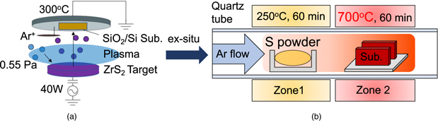
Fig. 1. (Color online) Schematics of (a) RF sputtering and (b) sulfur vapor annealing (SVA) conducted ex-situ.
Download figure:
Standard image High-resolution imageThe deposited ZrS2 films were subsequently subjected SVA [Fig. 1(b)]. The sulfur powder source was placed in the first zone, which was heated at 250 °C, and the sample wafer was placed in the second zone, which was heated at 700 °C, for 60 min under flowing Ar at 100 Pa. When the samples were transported between the sputtering and SVA apparatuses, they were exposed to air (Fig. 1). Two samples prepared with and without SVA were compared by X-ray diffraction (XRD), cross-sectional transmission electron microscopy (xTEM), and XPS analyses. The take-off angle of XPS was set to 45◦, and the XRD measurements were conducted out-of-plane.
2.2. Effects of high-k film deposition onto ZrS2 film
To clarify the effect of a high-k deposited film on the threshold voltage, we measured the surface potential of ZrS2 films, which is closely related to the threshold voltage. On the sample subjected to SVA in Sect. 2.1, two kinds of high-k film (Al2O3 and HfO2) was respectively deposited by ALD at 250 °C from 0 to 4 nm in 1 nm steps, resulting in a total of nine samples. Tetrakis(dimethylamido)hafnium(IV) (TDMAH) and H2O were used as precursors to deposit HfO2 films, and trimethylaluminum (TMA) and H2O were used as precursors to deposit Al2O3 films. The sample with a 0 nm high-k film was only heated for 15 min at 250 °C to stabilize the substrate temperature. During transport between the SVA and ALD apparatuses, the samples were exposed to air. The nine prepared samples were compared by XPS analysis.
2.3. Further enhancement of ZrS2 films by changing process sequence
We attempted to further enhance the quality of ZrS2 films by changing the sequence of the SVA and ALD methods mentioned in Sects. 2.1 and 2.2. In preliminary experiments, we investigated whether an ultra-thin (e.g. 1 nm) high-k film could be deposited uniformly, which is the premise for the present work. A ZrS2 film was deposited under the same conditions used in Sect. 2.1, and a 1 nm thick Al2O3 film was then deposited onto the ZrS2 film at 150 °C. The 1 nm thick Al2O3-coated ZrS2 film and the ZrS2 film before deposition of the Al2O3 were compared by AFM analysis.
Next, the sample with a deposited 1 nm thick Al2O3 film was subjected to SVA for 40 min; that is, the sequence of SVA and ALD was reversed. In addition to this sample, a sample annealed under an Ar atmosphere instead of being subjected to SVA and a sample subjected to SVA before deposition of a 1 nm thick Al2O3 film were also prepared; the three samples were subsequently compared by XPS and the Raman spectroscopy.
3. Results and discussion
3.1. Effects of SVA on ZrS2 film
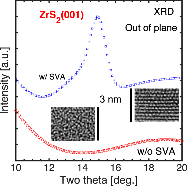
The XRD patterns and xTEM images are shown in Fig. 2. A peak attributed to ZrS2 (001) was observed only in the XRD pattern of the sample subjected to SVA. 22) Because the appearance of the ZrS2 (001) peak suggests the existence of a layered ZrS2 film, we inferred that the ZrS2 film was layered as a result of SVA. In addition, the xTEM images show that the ZrS2 film not subjected to SVA is amorphous, whereas that subjected to SVA is crystallized (layered), consistent with the XRD results. In MoS2 film, the film deposited by sputtering was crystalline and SVA enhanced its crystallinity; 15) however, in the case of ZrS2 film, our results clarify that SVA not only enhanced crystallinity but also induced crystallization.

Fig. 2. (Color online) XRD patterns and cross-sectional TEM images of ZrS2 films prepared with and without SVA.
Download figure:
Standard image High-resolution imageThe XPS spectra of Zr 3d in Fig. 3(a) show two peaks attributable to Zr–S and Zr–O bonds in zirconium compounds and indicate that the Zr–O/Zr–S ratio increases after SVA. 23,24) Because zirconium does not evaporate at 700 °C, which was the maximum temperature used in the present work, the Zr–S/Zr–O ratio represents the thickness ratio of ZrSx /ZrOx films under the assumption that the films are uniform. Therefore, SVA is considered to increase the thickness of the zirconium sulfide film, resulting in a thinner oxide film. This result suggests that the thickness of the oxide film (i.e. the interfacial layer) can be controlled by SVA. The S 2p XPS spectra in Fig. 3(b) show S2–Zr peaks (indicating the existence of ZrS3) only for the sample not subjected to SVA. 25) Upon initial inspection, the spectra of the sample not subjected to SVA appear to show a single peak attributable to S–Zr; however, the agreement of fit is poor in this case. Compared with zirconium and sulfur atoms, sulfur atoms have a smaller surface area and therefore a longer mean free path. In this regard, we considered that a sulfur-rich zirconium sulfide film, i.e. a mixed film of ZrS2 and ZrS3, was formed because more sulfur atoms reached the substrate. However, the S2–Zr peak disappeared after SVA. This result suggests that ZrS3 was pyrolyzed by SVA given that ZrS3 pyrolyzes to ZrS2 under sputtering conditions at 700 °C and 0.55 Pa. However, even if ZrS3 is not completely pyrolyzed and some remains, it is not a fatal issue because crystallized ZrS3 has a pseudo-one-dimensional structure and an appropriate bandgap as a semiconductor. 26) In addition to the bonding peak from sulfide, S–S bonding peaks are observed in the spectra of the sample subjected SVA, which might be due to sulfur deposited onto the surface after SVA. The O 1s XPS spectra in Fig. 3(c) show O–H bond peaks in addition to the O–Zr bond peaks originating from the zirconium oxide film. The abundance of O–Zr bonds is expected to decrease with a reduction in the oxide film thickness, as previously described; however, the abundance of O–H bonds is observed to decrease more than expected. Some of the O–H bonds are considered to originate from contamination-derived materials; however, these peaks are expected to be mainly due to the hydroxylation of zirconium. The hydroxylation of zirconium is assumed to occur as a result of unstable oxidation in the air after sputtering; however, as in the case of ZrS2, the zirconium hydroxide is considered to be removed by pyrolysis during SVA. Also, Fig. 3 as a whole shows that, after SVA, the peak positions shift to the higher-energy side. Because sulfur defects have been reported to be compensated by SVA and result in a shift of the peak position, 17) we also attribute the peak shift in this case to sulfur compensation or crystallization.

Fig. 3. (Color online) XPS spectra of (a) Zr 3d, (b) S 2p, and (c) O 1s in ZrS2 films prepared with and without SVA.
Download figure:
Standard image High-resolution imageThe stoichiometric ratio of each compound, as calculated from the XPS analysis results, is reported in Table I. Only the peaks derived from bonding with the matching atom (e.g. S/Zr means the ratio of S–Zr/Zr–S) were counted. The SVA process apparently resulted in a lower S/Zr ratio. This result appears to contradict the consideration that sulfur was compensated by SVA; however, it is explained by supposing that ZrS3 and ZrS2 with some sulfur defects were synthesized by sputtering and subsequently pyrolyzed by SVA, resulting in only ZrS2 with few sulfur defects. In addition, we found that the O/Zr ratio in the film subjected to SVA was nearly stoichiometric and stable. The heat applied during SVA is considered to pyrolyze the zirconium hydroxide, resulting in the formation of a high-quality zirconium oxide film. The much lower O/Zr ratio of 1.0 in the film not subjected to SVA is caused by not counting O–H bonds, which are assumed to be derived from zirconium hydroxide; that is, the "missing" oxygen is attributed to oxygen sites occupied by hydroxyl groups rather than to oxygen vacancies.
Table I. Stoichiometric ratio of each compound film calculated from the XPS analysis results.
| Ratio | w/o SVA | w/ SVA |
|---|---|---|
| S/Zr | 2.3 | 1.9 |
| O/Zr | 1.0 | 1.8 |
Figure 4 shows, on the basis of the previous discussion, how the zirconium sulfides and oxides were transformed. Because sulfur atoms can reach the substrate more easily than zirconium atoms as a result of their smaller surface area, a mixture of ZrS2 and ZrS3 is formed. When the film is exposed to the air, its surface is oxidized by the O2 in the air. Incomplete zirconium oxides with hydroxy groups are formed, and cationic defects are generated in zirconium sulfides because of the removal of sulfur. SVA induces thermal decomposition of ZrS3 and crystallization of ZrS2. Similarly, the zirconium oxide produced by surface oxidation is thermally transformed into ZrO2, which is favorable in terms of stoichiometry, and partly into ZrS2, which reduces the thickness of ZrO2 and enhances the thickness of ZrS2.

Fig. 4. (Color online) Possible transformation of ZrOx /ZrSx systems characterized by XRD and XPS: (a) as-deposited, (b) without SVA, and (c) with SVA.
Download figure:
Standard image High-resolution imageFrom the aforementioned viewpoint, the SVA is critical for producing ZrS2 by PVD. Optimizing the SVA conditions are future issues to be addressed to improve the quality of ZrS2 films.
3.2. Effects of depositing high-k film onto ZrS2 film
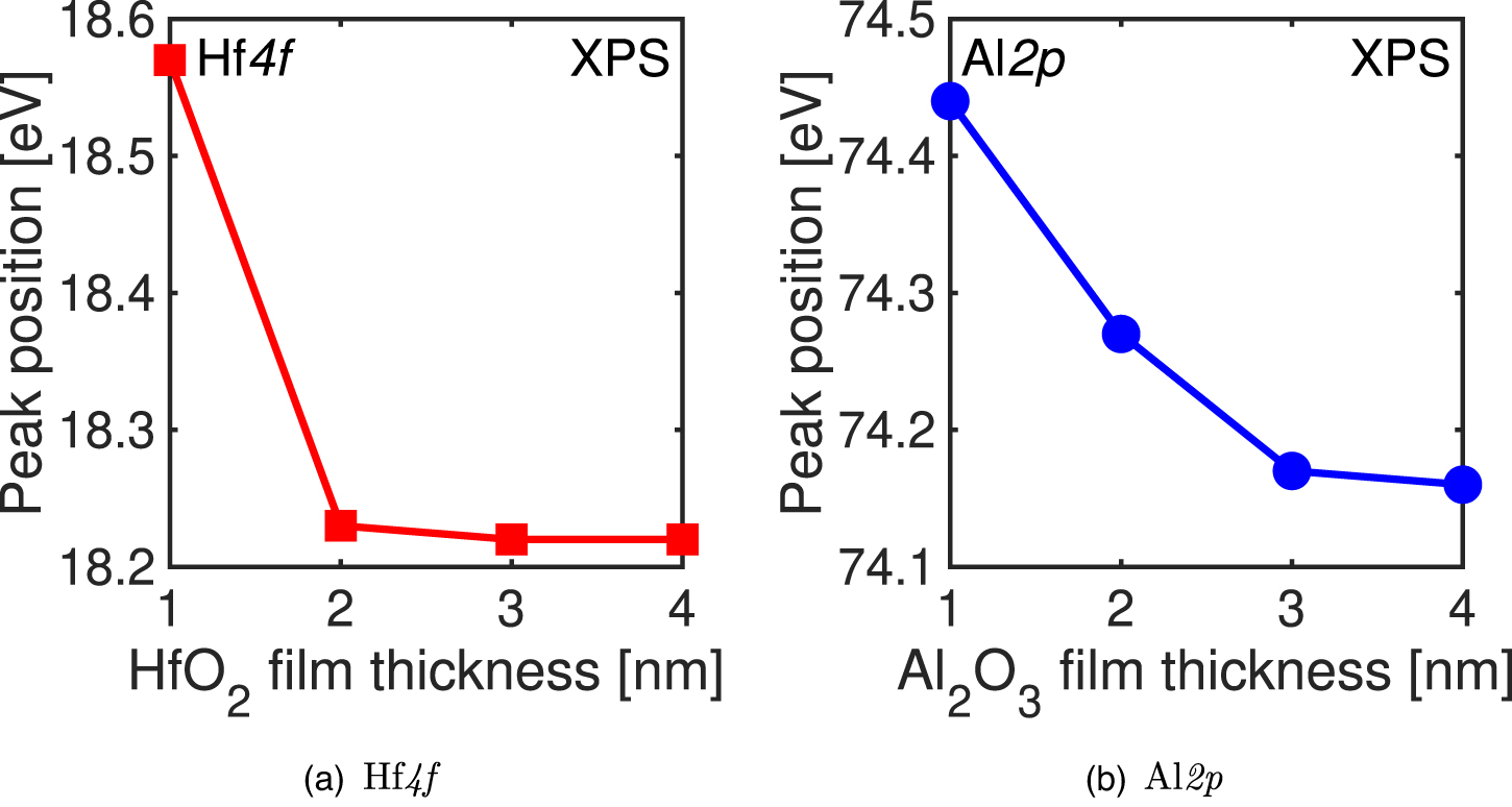
Figures 5(a) and 5(b) show the high-k film thickness dependence of the peak position energies (PPEs) derived from the cation of the high-k film by peak fitting the XPS spectra. 27,28) With the scaling of the high-k film, the influence of the high-k/ZrO2 interface increases, which suggests that the PPE of the high-k film is shifted to higher energies as a result of its deposition. By contrast, an increase in the film thickness weakens the effect of the interface, resulting in a PPE that approaches the value of the bulk high-k material. 27,28) Therefore, the PPE of the high-k cation at the interface in the thick high-k film cannot be determined from Fig. 5.

Fig. 5. (Color online) Peak position energies (PPEs) in (a) Hf 4f and (b) Al 2p XPS spectra, plotted as functions of high-k film thickness.
Download figure:
Standard image High-resolution imageFigure 6 shows the PPEs of S 2p from ZrS2 as functions of the high-k film thickness; 23) the trends for the samples with Al2O3 and HfO2 films diverge at a film thickness of 2 nm. In contrast to Fig. 5, Fig. 6 shows the PPEs at the interface for all high-k film thicknesses, i.e. it can be said to illustrate the PPE dependence on high-k film thickness. When a 4 nm thick HfO2 film was deposited, the peak intensity of S 2p derived from ZrS2 was weak and the PPE could not be calculated. When the thickness of the high-k film was less than 2 nm, the PPE shifted to the lower-energy side for both high-k films as a result of their deposition. Collectively, the results show that deposition of a high-k film with a thickness of 2 nm or less results in PPE shifts in different directions for the ZrS2 film and the high-k film.
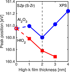
Fig. 6. (Color online) PPEs of S 2p from ZrS2 in the XPS spectra, plotted as functions of the high-k film thickness.
Download figure:
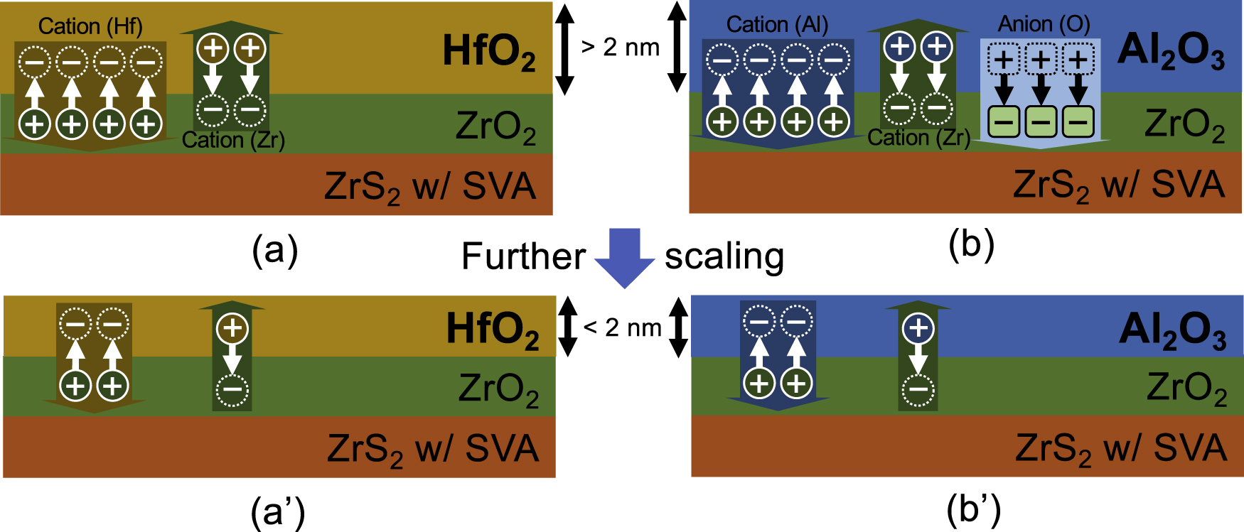
Standard image High-resolution imageWe speculate that interface dipoles are formed by the diffusion of cations between the zirconium compound and the high-k film. Interface dipoles are known to form by the migration of oxygen atoms due to the difference in surface oxygen atom density between the films; 29) however, another literature also reports on interface dipoles formed by the migration of cations. 30,31) In this case, we considered the interface dipole to have formed by the diffusion of cations from the high-k film to the zirconium compound side. When the HfO2 film was thicker than 2 nm, the magnitude of the shift in the S 2p peaks increased with an increase in the HfO2 film thickness, which suggests that the concentration of interface dipoles is proportional to the HfO2 film thickness, at least for films with a thickness of 3 nm or less. When the thickness of the Al2O3 film was greater than 2 nm, the direction of the shift was reversed. This behavior is attributed to the formation of another type of interface dipole by the diffusion of oxygen between Al2O3 and ZrO2. As previously discussed, the interface dipoles due to oxygen have been reported to be formed as a result of the difference in surface oxygen atomic density between the films. 29) A comparison of the surface oxygen atomic density of Al2O3 and ZrO2 suggests that oxygen diffuses from Al2O3 to the ZrO2 side to relax the difference density and form interface dipoles because Al2O3 has a higher surface oxygen atomic density than ZrO2. A certain thickness of Al2O3 film has been reported to be necessary to form interface dipoles via the diffusion of oxygen from Al2O3, supporting the present results. 32) However, the similar surface oxygen atomic density of HfO2 and ZrO2 systems indicates that oxygen diffuses equivalently and that no interface dipoles due to oxygen were formed.
Figure 7 summarizes the discussion thus far in terms of scaling the high-k film thickness. When the high-k film is thicker than 2 nm, the surface potential shifts depending on the high-k material because of the different types of interface dipoles caused by the diffusion of oxygen or cations. Given that the surface potential is closely related to the threshold voltage, the results support that the shift of the threshold voltage depends on the high-k material. However, when the high-k film is less than 2 nm thick, the shift of the surface potential is suppressed with the scaling of the high-k film. To continue the scaling of the high-k film, the shit in threshold voltage would be minor.

Fig. 7. (Color online) Possible model of dipole formation due to the deposition of (a)/(a') HfO2 and (b)/(b') Al2O3 films onto ZrS2 films. Dotted circles show vacancies after diffusion shown by a wide arrow, for each cation and anion. Arrow lines also represent electric force.
Download figure:
Standard image High-resolution image3.3. Further enhancement of ZrS2 films by changing process sequence
Figures 8(a) and 8(b) show the AFM images and the root mean square (RMS) roughness values calculated from the images. In the case of MoS2 film, it has been reported that the RMS roughness increases after deposition of a 1 nm high-k film by ALD because dangling bonds are nucleation sites; 11) however, the RMS roughness did not increase in this experiment. In the case of ZrS2, as shown in 3.1, an amorphous ZrO2 film is formed on the surface, which is considered to enable uniform deposition of ultra-thin high-k films by ALD.

Fig. 8. AFM images of ZrS2 surfaces (a) as-deposited and (b) after deposition of a 1 nm Al2O3 film.
Download figure:
Standard image High-resolution imageFigure 9 shows the Raman spectra and the full-width at half-maximum (FWHM) of the A1g peak in a ZrS2 film. 12) In the spectrum of the sample subjected to SVA, A1g and A2u peaks derived from the ZrS2 film are observed; by contrast, in the spectrum of the sample prepared with Ar annealing, only peaks derived from the Si substrate are observed. 12) We considered that annealing under Ar accelerated the desorption of sulfur from the ZrS2 film, resulting in oxidation to an amorphous zirconium oxide film upon exposure to the air. Because the Ar-annealed sample was annealed after ALD, it had a 1 nm Al2O3 passivation film on its surface; however, we speculate that it was desorbed through the 1 nm Al2O3 passivation film. A comparison of samples subjected to SVA reveals that SVA after ALD narrowed the FWHM, indicating better crystallinity. If the high-k film is deposited after SVA as before, the zirconium compound film is directly exposed to the air after SVA, which can lead to degradation of its crystallinity by sulfur desorption and oxidation of zirconium. However, deposition of the high-k film before SVA prevents direct exposure of the zirconium compound film to the air after SVA, likely preventing the degradation of ZrS2 crystallinity.
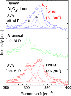
Fig. 9. (Color online) Raman spectra of Al2O3/ZrS2 film stacks subjected to SVA after/before deposition of 1 nm ALD-Al2O3 and Ar annealing.
Download figure:
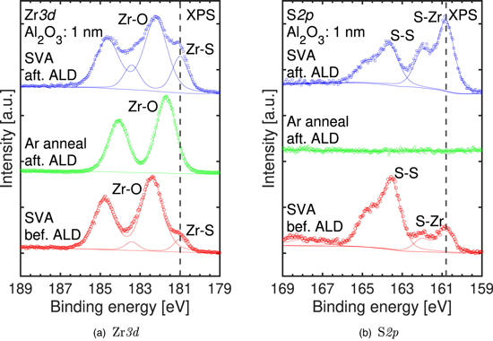
Standard image High-resolution imageThe Zr 3d XPS spectra in Fig. 10(a) show a peak derived from the ZrS2 film only for the sample subjected to SVA. 23,24) A comparison of the XPS results for samples subjected to SVA indicates that the Zr–O/Zr–S ratio increases when the SVA is performed even after the ALD process. Consistent with Sect. 3.1, we speculated that the thickness of the ZrS2 film was enhanced by SVA after ALD. Collectively, the XPS and Raman spectral analysis results clarify that the 1 nm Al2O3 passivation film protects the zirconium compound from being exposed to the air after SVA, thereby preventing not only the degradation of its crystallinity but also an increase of the oxide film thickness due to sulfur desorption and oxidation of zirconium. Figure 10(b) shows the S 2p XPS spectra; no peaks are observed in the spectrum of the sample subjected to Ar annealing. Combined with the result that no ZrS2-derived peaks were observed in the Zr 3d XPS spectra, this analysis indicates that Ar annealing removes all the sulfur and results in only a zirconium oxide film, consistent with the results of the Raman spectral analysis. More importantly, a comparison of the samples subjected to SVA reveals that the peak position changed by only 0.1 eV because of the difference in the SVA sequence, indicating that the SVA after ALD enhances the thickness and crystallinity without influencing the surface potential.
Fig. 10. (Color online) (a) Zr 3d and (b) S 2p XPS spectra of Al2O3/ZrS2 film stacks subjected to SVA after/before deposition of 1 nm ALD-Al2O3 and Ar annealing.
Download figure:
Standard image High-resolution image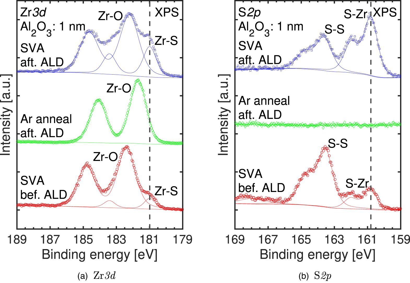
4. Conclusions
The SVA has the following effects: it (1) compensates for sulfur defects, (2) pyrolyzes ZrS3 to crystallize ZrS2, (3) decreases the thickness of ZrO2 films and increases the thickness of ZrS2 films, and (4) improves the quality of ZrO2 films. Thus, the SVA is essential for fabricating high-quality PVD-ZrS2 films. In addition, the change in surface potential of a ZrS2 film because of interface dipoles between the high-k and zirconium compound films is suppressed with scaling of the high-k film thickness. Furthermore, the SVA through the high-k film enhances the quality of the ZrS2 film without influencing the surface potential, possibly enabling control of the threshold voltage in a ZrS2 MISFET. With optimization of the SVA and high-k film deposition processes, we expect that high-quality, normally off ZrS2 MISFETs can be fabricated.
Acknowledgments
Our measurements were supported by the Open Facility Center, Tokyo Institute of Technology. This work was partly supported by JSPS KAKENHI Grant Number 20H05880.