

Abstract
We extract the electric properties of border traps with long time constant in low-pressure chemical vapor deposition (LPCVD) Si3N4/GaN/AlGaN/GaN metal–insulator–semiconductor (MIS) structure using quasi-static capacitance voltage method. The energy and depth distribution of the border traps is calculated based on the analysis of energy band diagram and charging dynamic of border traps in the MIS structures. With this method, it is found that LPCVD Si3N4/GaN/AlGaN/GaN MIS structure have a high density of border traps in the order up to 1021 cm−3 eV−1 located at energy level between EC,GaN − 0.04 eV and EC,GaN − 0.66 eV with distance of 1.0–4.2 nm from the Si3N4/GaN interface. Microstructure analysis suggests that the high density of border traps is possibly correlated to the oxygen content at the Si3N4/GaN interface. Meanwhile, the proposed method is also suitable for MIS or metal-oxide-semiconductor structure on other semiconductors, providing another powerful tool to analysis the physical properties of border traps.
Export citation and abstract BibTeX RIS
1. Introduction
Benefitting from the unique material properties, AlGaN/GaN based electronic devices have been paid much attention in the past several years. 1,2) Among these, AlGaN/GaN metal–insulator–semiconductor (MIS) or metal-oxide-semiconductor (MOS) high electron mobility transistors (HEMT) have the advantages of low gate leakage and large gate swing. 3–5) In such devices, the trap states near the insulator/semiconductor interface have an important effect on the device performance, such as the transport properties of carriers in the channel, positive bias temperature instability, subthreshold voltage swing, etc. Meanwhile, (Al)GaN does not have a high quality native oxide as that in SiO2/Si system. In-situ and ex-situ gate dielectrics, such as Si3N4, SiO2, Al2O3, have been grown with chemical vapor deposition (CVD) or atomic layer deposition for GaN MISHEMT. 6–8) It is generally recognized that the interface trap density is much higher in MOS or MIS structures with III–V channel than that in SiO2/Si MOS structure. Besides the interface traps, there is another type of trap, named border trap with long time constant, existing in such structure. Border traps are located in the gate dielectric close to the dielectric/semiconductor interface. 9) Liu et al. found that the density of border traps could be suppressed by the AlN interfacial layer in Al2O3/AlN/GaN MOS structure. 10) Sun et al. studied the gate oxide traps in HfO2/AlGaN/GaN MOSHEMT using ac transconductance method. 11) Wu et al. found that Vth shift of GaN MISHEMT during a positive gate bias stress is highly correlated to not only interface states but also border traps in the dielectric. 12) Yin et al. found that the properties of border traps are correlated to the gate recess method in gate recessed normally-off Al2O3/GaN MOSFET using low frequency noise analysis. 13) Ramanan et al. proposed a pulsed IV measurement to characterize the interface states and border traps. 14) Gao et al. used a high speed spot-Id measurement to calculate the energy distribution of border traps in AlGaN/GaN MIS-HEMT. 15) Nevertheless, there are few methods which could analytically extract the energy and depth dependent density of border traps in GaN electronic device with insulated gate structure.
Previously, we have grown Si3N4 using high temperature low pressure chemical vapor deposition (LPCVD) method as gate insulator in AlGaN/GaN MISHEMT. 16) The LPCVD grown Si3N4 features low leakage current and high breakdown field. However, directly grown Si3N4 on AlGaN/GaN heterostructure would lead to a rough Si3N4/(Al)GaN interface and a high interface trap density. 16) The stability of threshold voltage during positive gate bias stress was also found to be directly related to the properties of interface related trap states. 17) In this work, we study the electric properties of border traps in Si3N4/GaN/AlGaN/GaN MIS structure using the quasi-static capacitance–voltage (QSCV) method, 18) which is capable of probing the traps with long time constant. The energy and spatial distribution of border traps is extracted quantitively by calculating the energy band diagram and trap occupation dynamics. It is found that LPCVD Si3N4/GaN/AlGaN/GaN MIS structure has a high density of border traps in the order up to 1021 cm−3 eV−1 located at energy level between EC,GaN − 0.04 eV and EC,GaN − 0.66 eV with a distance of 1.0–4.2 nm from the Si3N4/GaN interface, possibly induced by surface oxygen contamination during high temperature process.
2. Experiment and method
The HEMT structure used in this work is grown by metal organic chemical vapor deposition (MOCVD), which consists a 4 μm C-doped semi-insulating (Al)GaN buffer layer, a 300 nm i-GaN channel layer, a 1 nm AlN layer, a 25 nm i-Al0.25Ga0.75N barrier layer and 3.4 nm GaN cap layer. The device process started with the 35 nm thick Si3N4 layer deposition using LPCVD at 730 °C, which was proven to feature high breakdown field and low leakage current. 19,20) Ti/Al/Ti/TiN multilayer were used as the ohmic contact after high temperature annealing. The thick SiO2 passivation layer was grown by PECVD. The anode metal of the MIS structures was formed by metal deposition and etching after removing the SiO2 passivation layer in the anode area using a combination of dry and wet-etching. The circular MIS structure under test features a diameter of 100 μm. The distance between the anode and the cathode is 15 μm. Figure 1 shows the schematic cross section view of the fabricated MIS structures. The optical image of the fabricated device is also shown in the insert of Fig. 1. AC capacitance and conductance curves were measured with Keysight MFCMU in B1500A, Keysight E4980A and Cascade Microtech 12 K probe station. The amplitude of the ac small signal is 30 mV. QSCV is measured using step voltage method with HRSMUs in Keysight B1500A semiconductor parameter analyzer. The amount of the charge ∆Q is obtained by integrating the transient current over a certain time after the voltage step. The dc bias is swept from −15 V to 6 V with a step of 200 mV. The bias is hold for 20 s before measuring QSCV to insure that the traps with a time constant below 10 s could effectively responses during the QSCV measurement step. The step voltage for measuring QSCV is 100 mV.

Fig. 1. (Color online) The schematic cross section view of the LPCVD Si3N4/GaN/AlGaN/GaN MIS structure. The insert shows the optical image of the MIS capacitor.
Download figure:
Standard image High-resolution image3. Result and discussion
3.1. High frequency CV measurement
Figure 2 shows the measured HF capacitance voltage (C–V) and conductance voltage (G/ω–V) curves of the MIS structure at frequencies of 1 kHz and 1 MHz. The dc bias sweeping direction is from negative to positive and then back with a sweep rating of 0.1 V s−1. The theoretical low frequency curve without traps calculated without considering quantum effect is also shown for comparison. From the theoretical curve, it can be seen that two sharp rising of capacitance corresponding to the formation of 2DEG and the spillover of electrons in the GaN cap layer are observed. It should be noted that the second rise could also be induced by the response of trap states at the Si3N4/GaN interface. 21,22) However, the second rising is not observed in experimental C–V curves even up to 6 V for both frequencies. The lack of the second rise of capacitance suggests that there are high density of deep trap near the Si3N4/GaN interface. The large density of deep trap states near the interface would pin the surface Fermi level at a certain energy level below the conduction band of GaN and prohibit the communication of carriers between the 2DEG channel and the interface. The lack of the G/ω–V peak in positive bias also proves the above analysis as no loss would be observed if the carriers does not response to the ac signal. Meanwhile, those trap states responsible for the flat C–V curve in positive bias would not response at 1 kHz and the time constant should be larger than 1 ms. Those traps would most likely to be the border traps, which have a relatively long time constant.

Fig. 2. (Color online) Bidirectional high frequency capacitance voltage and conductance voltage curves of the MIS structure measured at frequency of 1 kHz and 1 MHz. The theoretical low frequency CV curve without interface related traps are also shown for comparison.
Download figure:
Standard image High-resolution image3.2. Quasi-static CV measurement
The results in Fig. 3 are measured with the following sequences: QSCV with integration time from 50 ms to 10 s, and AC–CV curves with frequencies of 20 Hz, 100 Hz, 1 kHz and 1 MHz. With high positive gate bias, part of trapped carriers with extremely long time constant would not be emitted even after 5 min relaxation between each measurement, which could contribute to the shift between QSCV and AC–CV curves.

Fig. 3. (Color online) QSCV curves of the Si3N4/GaN/AlGaN/GaN MIS structure. The integration time is from 50 ms up to 10 s. The AC–CV curves are also shown for comparison.
Download figure:
Standard image High-resolution imageIt can be seen in Fig. 3 that the second rising of capacitance is already observed with 50 ms integration time during QSCV measurement. The quasi-static capacitance in the second rising continuously increases with the integration time from 50 ms to 10 s, suggesting a broad distribution of border traps. For AC–CV measurement, there is also signs of the second rising of capacitance at ac frequency of 20 Hz. The measured AC–CV curves at low frequency is noisy due to the small ac current as the capacitor under test is smaller than 15 pF. The equivalent ac frequency for an integration time of 50 ms in QSCV measurement is  From Fig. 3 it can be seen that the measured QSCV and HFCV capacitance values are continuous as a function of measurement frequency, suggesting that the QSCV measurement is effective in probing trap states, especially the one with long time constant.
3.3. Extract the properties of border traps from QSCV for elastic tunneling process
Figure 4 shows the conduction band diagram of the Si3N4/GaN/AlGaN/GaN MIS structures. EFs is the location of Fermi level in the semiconductor layer. EFm is the location of Fermi level of the anode metal. For the border traps distributed with a distance x from the Si3N4/GaN interface, the capture cross section  is reduced by the factor
  when viewed by an electron at the GaN surface from the quantum tunneling theory if the tunneling process is elastic,
23,24)
when viewed by an electron at the GaN surface from the quantum tunneling theory if the tunneling process is elastic,
23,24)

where  is the capture cross section of the interface traps (located with distance 0 from the interface) and λ is the insulator tunneling attenuation distance defined as
  m* is the electron effective mass of the insulator and
  is the barrier height from the energy level of interface traps to the conduction band of Si3N4 layer.

Fig. 4. (Color online) Schematic band diagram of the metal/Si3N4/GaN/AlGaN/GaN MIS structure. In the current figure, the energy level of border traps is defined as the energy difference from the conduction band edge of GaN layer. In the QSCV measurement, the border traps located within δE = E1 − E2 would be probed in a voltage step Va,2 − Va,1 = 0.1 V if the time constant τ of the border traps is smaller than the integration time.
Download figure:
Standard image High-resolution imageThen the time constant of the border trap τ (mean time before the trap captures an electron) is expressed as,


where τ0 is the time constant of traps at the interface,  is the thermal velocity of electrons. NC
is the density of states of the conduction band. ET
is the energy level of the interface traps relative to the conduction band of GaN layer. The probing depth boundary xm within which the traps would response can be expressed as:
is the thermal velocity of electrons. NC
is the density of states of the conduction band. ET
is the energy level of the interface traps relative to the conduction band of GaN layer. The probing depth boundary xm within which the traps would response can be expressed as:

where τm is the integration time during QSCV measurement. The trapped charge δQ in the energy range δE from E1 to E2 is

where Nt(x) is the border trap density in unit of cm−3 eV−1 and E is the energy level of the traps relative to the conduction band of GaN. The depth and energy distribution Nt of border traps could be extracted from the integration time dependent quasi-static capacitance C by,


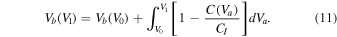
where V is the dc bias during QSCV measurement. In order to accurately calculate δE and the energy level E relative to the conduction band edge of GaN, we adopted the method proposed by C. N. Berglund in SiO2/Si system. 25) It can be seen in Fig. 4 that

where Va is the voltage applied on the anode, VI is the voltage drop on the insulator, Vb is the voltage drop on the barrier layer (including AlGaN layer and the GaN cap) and ψs is the surface potential of the channel layer. If the 2DEG channel is in accumulation and degenerated in the sweeping range of Va, ψs would not change much with the anode bias and  could be neglected. Then, the measured capacitance could be expressed as

where CI is the capacitance of the insulator layer.
Hence,

Then,  could be calculated by integration Eq. (10) with the QSCV curve measured at an integration time of 20 s, supposing that all the traps would response
It can be seen that Eq. (11) is similar with the situation in SiO2/Si system, 25) taking advantage of the degenerated 2DEG in AlGaN/GaN heterostructure. The trap energy level E at a certain Va is directly correlated to Vb by

where  is the conduction band offset between AlGaN and GaN, E
n
is the distance between the conduction band and the Fermi level in the GaN buffer. Due to the complication of the 2DEG system, it is difficult to match the experimental curve of
is the conduction band offset between AlGaN and GaN, E
n
is the distance between the conduction band and the Fermi level in the GaN buffer. Due to the complication of the 2DEG system, it is difficult to match the experimental curve of  versus Vb and the theoretical curve assuming no trap states in the strong accumulation region as is done in SiO2/Si system.
25) Alternately, we chose V0 as 0 V and E(0) could be calculated from the 2DEG density extracted from HF curves by solving the self-consistent Poisson's equation. The theoretical net negative charge at the GaN/Al0.25Ga0.75N interface and and positive charge at the Al0.25Ga0.75N/GaN interface induced by polarization effect is set to be 1.05 × 1013 cm−2. In our calculation, the net charge at the Si3N4/GaN interface (including the surface donor traps and polarization induced charge) is tuned to fit the measured 2DEG density. The trap energy level at a certain bias Va could be calculated by,
versus Vb and the theoretical curve assuming no trap states in the strong accumulation region as is done in SiO2/Si system.
25) Alternately, we chose V0 as 0 V and E(0) could be calculated from the 2DEG density extracted from HF curves by solving the self-consistent Poisson's equation. The theoretical net negative charge at the GaN/Al0.25Ga0.75N interface and and positive charge at the Al0.25Ga0.75N/GaN interface induced by polarization effect is set to be 1.05 × 1013 cm−2. In our calculation, the net charge at the Si3N4/GaN interface (including the surface donor traps and polarization induced charge) is tuned to fit the measured 2DEG density. The trap energy level at a certain bias Va could be calculated by,

The prerequisite of Eq. (9) is also satisfied as the lower limit of the integration (V0) is 0 V and the 2DEG is degenerated from 0 to 6 V. Once we got the bias dependent trap energy level E(Va), then the barrier height  influencing the attenuation length λ in Eqs. (1) and (2) could be calculated by
  where
where  is the conduction band offset between Si3N4 and GaN. Figure 5 shows the calculated
  and attenuation length λ as a function of bias with the equations above.

Fig. 5. (Color online) Calculated  and attenuation length λ as a function of bias.
Download figure:
Standard image High-resolution imageFigure 6 shows the distribution of border traps extracted using Eqs. (6), (7), (11) and (13). There are high density of border traps up to an order of 1021 cm−3 eV−1 located at energy level between EC,GaN − 0.04 eV and EC,GaN − 0.66 eV with a distance of 1.0–4.2 nm from the Si3N4/GaN interface. The extracted value is comparable with the 1013–1014 cm−2 eV−1 in the work of Ramanan et al., supposing that the border traps are distributed in several nanometers from the interface. 14)

Fig. 6. (Color online) Calculated energy and depth distribution of border traps in the LPCVD Si3N4/GaN/AlGaN/GaN MIS structure supposing that the tunnelling process is elastic.
Download figure:
Standard image High-resolution image3.4. Temperature dependent QSCV measurement
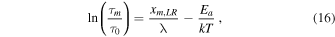
Figure 7 shows the temperature dependent QSCV curves of the MIS structure from 25 °C to 70 °C. The capacitance in the second rise region is positive temperature dependent and the behaviour is more obvious at low integration time, suggesting that the capture process is thermal activated. In our experiment, the time constant is much larger than that of the interface states and we attribute the response in QSCV measurement to border traps in the Si3N4 layer close to the Si3N4/GaN interface. The charge exchange between the border trap and interface states is initially supposed to be based on the elastic tunneling mechanism, which is weak temperature dependent. The observed thermal activation behavior in QSCV measurement could be explained if the tunneling process is not elastic and there are lattice relaxation during trapping.
26,27) The electron–phonon interaction could be illustrated using the coordinate diagram. Figure 8 shows the configuration-coordinate diagram of the border traps featuring lattice relaxation after trapping.
26,28,29) The energy barrier for electron capture and emission between neutral and occupied states is Ea and Eb, respectively. For the trap time constant and capture cross section calculation, we used the formulation proposed by C. H. Henry and D. V. Lang.
28) The capture cross section  considering the lattice relaxation is expressed as,
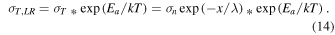

Fig. 7. (Color online) Temperature dependent QSCV curves of the Si3N4/GaN/AlGaN/GaN MIS structure from 25 °C to 70 ºC. The integration time during QSCV measurement in (a) and (b) is 500 ms and 5 s, respectively.
Download figure:
Standard image High-resolution image
Fig. 8. Configuration coordinate diagram of the border traps featuring lattice relaxation after trapping.
Download figure:
Standard image High-resolution imageThen, the time constant of the border trap considering the lattice relaxation could be expressed as:

The thermal activated capture cross section and smaller time constant would lead to the increased QSCV capacitance at high temperature due to thermal enhanced trapping during integration time τm.
28–30) From Eq. (15) we can calculate the probing depth  of the border traps with lattice relaxation,

Comparing Eq. (17) with (4), it can be seen that the probing depth of the border trap is shifted by a constant  if we know the activation energy Ea. If the capture cross section is not thermal activated (Ea = 0), we can see that Eq. (17) is reduced to Eq. (4). The calculation is self-consistent. The current work mainly focused on the methodology to extract the properties of border traps using QSCV measurement. The calculation of activation energy for carrier capture after tunneling is our further work. For the device under test in this study, the actual distribution of border traps is a redrawn figure of Fig. 6 by replacing the title of x axis with
  or shift the tick label of x axis by
  The probing depth is deeper.
3.5. Discussion
Previous, it was found that directly grown LPCVD Si3N4 on (Al)GaN surface would lead to a disorder interface between Si3N4 and (Al)GaN, possibly induced by the H erosion effect during growth. 16) The contamination of the GaN surface before extrinsic dielectric growth may also induce trap states. Figure 9 shows the energy-dispersive X-ray (EDX) spectroscopy of the Si3N4/GaN/AlGaN interface. It can be found that the O centration is relatively high close to the Si3N4/GaN interface. It has also been reported that the Ga–O component is higher at the surface in an ICP etched GaN surface, which lead to a high density of border traps in gate recessed Al2O3/GaN MOSFET. 13) The result suggests that in situ or early surface protection should be adopted to reduce the density of border traps.

Fig. 9. (Color online) Energy-dispersive X-ray spectroscopy at the interface of the LPCVD Si3N4/GaN/AlGaN/GaN MIS structure.
Download figure:
Standard image High-resolution image
Finally, we would like to briefly discuss the feasibility of the proposed method in extracting the properties of border traps in GaN MIS structure with buried channel. In AlGaN/GaN MIS structure, the interface traps could not directly exchange carriers with the channel due to the existence of the AlGaN barrier. The electrons in the 2DEG channel could transport through the AlGaN barrier layer and be captured by the interface related traps if the position of the trap energy level is lower than the Fermi level. The charging and discharge time constant of the carriers between the surface channel and 2DEG channel may range from μs to ms due to the large conduction band offset and polarization enhanced barrier. 31) In the above analysis, the rising of the second slope is supposed to be induced solely by the charging of trap states. However, electrons could also be accumulated in the surface of GaN cap layer at high enough bias and induce the rising of capacitance. The proposed method stands for the results measured with long integration time, such as 50 ms and above in this work, as the charging and discharge time of free electrons in the barrier layer should be smaller. If one would like to detect border traps with characteristic time constant well below 50 ms, such as those close to the interface with energy level approaching the conduction band of GaN, directly calculating the trap density from the measured CV curves would overestimate the value. Meanwhile, Eq. (8) assumes that electrons does not spill over to the GaN cap. The upper limit of the integration V1 in Eq. (11) is limited not only by the thickness of Si3N4 and barrier layer, but also the density of interface related traps. The large density of border traps in the current device prohibit the formation of surface channel in the GaN cap layer and the aforementioned analysis could be performed.
4. Conclusion
In conclusion, we have studied the energy and depth distribution of border traps in LPCVD Si3N4/GaN/AlGaN/GaN MIS structure using QSCV measurement. It is found that there are high density of border traps in the order up to 1021 cm−3 eV−1 located at energy level between EC,GaN − 0.04 eV and EC,GaN − 0.66 eV with a distance of 1.0–4.2 nm from the Si3N4/GaN interface. Interface structure analysis indicates that the high Ga–O component near the Si3N4/GaN interface is the possible origin of the high density of border traps.
Acknowledgments
This work was supported by the National Key Research and Development Program of China under Grant 2017YFB0403000 and the National Natural Science Foundation of China under Grant 11634002 and Grant 61774002.