
Abstract
Dry film resists (DFRs) are suitable for the fabrication of large volume devices as the thickness of the film can be easily controlled. Here, the DFR microstructures were patterned using the proton beam writing (PBW) technique by taking advantages of the direct-write process, straight trajectories of protons, and large processing depth. The results show that the required irradiation dose of 15 μm DFR was 10 nC mm−2 for 1 MeV protons. In summary, we have optimized the PBW conditions to create smooth surface micropatterns with a vertical wall in the DFR.
Export citation and abstract BibTeX RIS
1. Introduction
Proton beam writing (PBW) is a direct lithographic method utilizing the characteristics of a MeV proton beam with straight trajectories and deep penetration depths (∼10–100 μm) into materials. Accordingly, the PBW technique can be employed to manufacture three-dimensional (3D) microstructures in μm thick photoresists such as SU-8 with a high-aspect-ratio, which is not feasible by using optical and electron beam lithographies. 1,2) In general, preparing a μm thick SU-8 film for micro-electromechanical systems (MEMS) and microfluidics involves multiple processing steps starting with spin coating the SU-8 liquid and subsequent soft bakings before exposure by PBW. 3–5) Though, the thickness of SU-8 film can easily be controlled by the spin coating process. 6) However, the thickness homogeneity is still an issue to be solved. 7–9) Furthermore, coating μm thick SU-8 on a flexible film is difficult with the conventional techniques by utilizing the liquid resist. 10)
To address this problem, a dry film resist (DFR), commonly utilized in printed circuit boards (PCBs), has been proposed to substitute the SU-8 liquid resist. 9) Utilizing the DFR offers several advantages. 7) Preparation of the DFRs on substrates or films requires only the lamination with the specified thickness, which the fabrication steps are decreased. 9) Furthermore, the DFR can provide higher thickness uniformity than the SU-8 film prepared by the spin coating. 7,9) Typically, 3D microstructures in the DFRs have been produced for various applications. For example, Nilsen et al. 11) demonstrated manufacturing the DFR micro-cantilever for atomic force microscopy (AFM). The waveguide microstructures for millimeter-wave were also produced in the DFRs, as reported by Farjana et al. 12) As presented by Wangler et al., 13) the Nickel gear was created by patterning the gear structure in the DFR and subsequently applying the Nickel electroplating. Additionally, the DFRs have been applied in microfluidic technology. Microfabrication in DFRs has been employed as the master molds for fabricating poly(dimethylsiloxane)/PDMS microfluidic devices using soft-lithography. 14–20) Moreover, Tsai et al. 21) demonstrated the applying DFR microfluidic channels in microchip capillary electrophoresis. The DFR microfluidic patterns were transferred to glass substrates by the wet etching method for microfluidic devices, as presented by Zhang et al. 22) The DFR micropatterns have been manufactured by photolithography, 23–25) UV-LEDs (light-emitting diodes) direct writing lithography, 26) direct projection lithography, 27) reactive ion etching and laser ablation, 28) and microscope-based maskless micropatterning technique. 16) However, according to the authors' best knowledge, the DFR has never been applied with the PBW.
In this work, we have investigated the applicability of using the DFR as the resist for the PBW technique. Applying the DFR to PBW could simplify the film preparation step and accelerate the development of MEMS and microfluidics. Therefore, we examined the sensitivity of the DFRs for 1 MeV protons and demonstrated the fabrication of microstructures in the DFRs using PBW.
2. Experimental methods
The DFR used in this experiment is a commercially available alkaline developing type with a thickness of 15 μm (Photec RY-5115, Showa Denko Materials Co., Ltd), covered with PE (polyethylene) and PET (polyethylene terephthalate) films on the top and bottom surfaces, respectively. Firstly, the PE film was removed, and then the DFR was laminated onto a 125 μm thick PET substrate with heating at 110 °C for 10 min to improve adhesion. A PET protective film on the surface of the DFR was removed before exposure by PBW. Subsequently, the micro-patterns in the DFRs were fabricated by means of PBW. The PBW was performed using a proton beam writer (Kobe Steel Corp., MB-S1000) at a beam energy of 1.0 MeV with a beam current of 15 pA. The beam diameter was estimated to be ∼1.2 μm using secondary electron imaging of a Cu mesh.
After proton beam writing, the exposed samples were developed in sodium carbonate (Na2CO3) solution of 1.0 wt% concentration at 30 °C and rinsed in purified water without and with applying ultrasonics to obtain the patterns. The surface and thickness of the fabricated 3D structures of the DFR were characterized by a laser microscope (OLS4000, Olympus) and a scanning electron microscope (JSM-6010LV, JEOL).
3. Results and discussion
To investigate the sensitivity of dry film resist (DFR), the micro-square patterns were irradiated with 1 MeV protons using the proton beam writing (PBW) technique at different doses, ranging from 0.1 to 100 nC mm−2. The time was varied from 30 s to 720 s to develop the irradiated samples in 1.0 wt% Na2CO3. It was found that 300 s was sufficient time for the sample development. We also observed from the results (not shown here) that the DFR in the unexposed areas was not completely dissolved in the development without applying ultrasonics. Therefore, ultrasonics was utilized to assist the developing process. Figure 1(a) shows a negative tone DFR resist behavior after development for 300 s under an ultrasonic cleaner. The microstructures were produced without observing the undissolved DFR in the unirradiated areas. This result suggests that ultrasonics is vital in the developing method for fabricating microstructures in DFR using the PBW approach. The responded DFR in the negative tone resist for the PBW demonstrated a similar behavior when the DFR was applied with other techniques, e.g. photolithography. In addition, an aqueous solution of Na2CO3, a typical DFR solvent utilized in photolithography, 14,17,20) can also be applied as the DFR developer in the PBW. However, the DFR developing procedure in the case of photolithography can be obtained without employing ultrasonics. As illustrated in Fig. 1(a), the micropatterns exposed to doses from 0.1 to 1.0 nC mm−2 were not observed. This result may suggest that the irradiation dose up to 1 nC mm−2 of 1 MeV protons is insufficient to produce the microstructures in the DFR. The micropatterns at 6, 30, and 100 nC mm−2 were also not visualized. This is because the DFR was peeled off from the substrate during the development process. The unusual removal of these DFR micropatterns might occur due to poor adhesion. The heights of the DFR micropatterns in Fig. 1(a) were measured with the laser microscope, as depicted in Fig. 1(b). It is found that the height increased with increasing the radiation dose. However, it is hard to observe the increasing height at the irradiation dose above 10 nC mm−2.
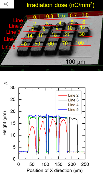
Fig. 1. (Color online) (a) The DFR micro-square patterns produced by 1 MeV protons at different doses from 0.1 to 100 nC mm−2 after development with utilizing ultrasonics for 300 s. Numbers indicate the irradiation dose in nC mm−2. The line indicates the measurement positions. (b) The surface profile measurement of the micropatterns in different scanning lines in (a).
Download figure:
Standard image High-resolution imageThe relationship between the height and the irradiation dose is illustrated in Fig. 2. The saturated height occurred at the irradiation dose ∼10 nC mm−2. Accordingly, the sensitivity of the DFRs at a thickness of 15 μm was 10 nC mm−2 for 1 MeV protons. Furata et al. 29) reported that 1.2 MeV protons at a fluence of 22 nC mm−2 were employed to fabricate microstructures in 50 μm thick SU-8. In addition, the sensitivity of SU-8 at a thickness of 5 μm was 30 nC mm−2 for 2.0 MeV protons, as presented by Sum et al. 30) As a result, it may imply that the required irradiation dose of the DFR is lower than that of SU-8 for PBW.
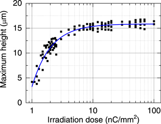
Fig. 2. (Color online) The plots between the DFR microstructure height (μm) and the irradiation dose (nC mm−2).
Download figure:
Standard image High-resolution imageThe applicability of utilizing the PBW method with the DFRs was further examined by fabricating circle, square, cross, and ring microstructures, as shown in Fig. 3(a). Figure 3(b) illustrates the micropatterns produced by 1 MeV proton at an irradiation dose of 40 nC mm−2 after development under the ultrasonic cleaner for 300 s. This irradiation dose was applied to ensure the fabrication. As indicated in the line in Fig. 3(b), the micropatterns' surface was scanned with the laser microscope, see Fig. 3(c), demonstrating the completed fabrication. Figure 4(a) depicts the SEM image of the microstructures in Fig. 3(b). It is seen that the surface of the DFR microstructures was smooth, and a vertical wall was observed in the SEM micrograph, as demonstrated in Fig. 4(b), due to the characteristics of the proton beam. Accordingly, the DFR can be applied to the PBW for manufacturing microstructures.

Fig. 3. (Color online) Circular, square, cross, and ring microstructures in the DFR produced by the PBW technique at the irradiation dose of 40 nC mm−2 after developing for 300 s in an ultrasonic cleaner. (a) Irradiation pattern design. (b) Optical image and (c) the surface profile of the patterns.
Download figure:
Standard image High-resolution image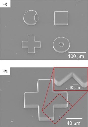
Fig. 4. (Color online) SEM images of (a) the microstructures in Figs. 3(b) and 3(b) a vertical wall of the pattern (tilt angle 30°).
Download figure:
Standard image High-resolution image
4. Conclusions
We have applied the proton beam writing (PBW) to fabricate dry film resist (DFR) microstructures. The sensitivity of the 15 μm thick DFR was determined at 10 nC mm−2 for 1 MeV protons. The development of the samples in the ultrasonic cleaner is required for fabricating microstructures with the PBW technique. The PBW can produce the micropatterns in the DFR with a smooth surface and a vertical wall. We found that DFR is fully applicable to PBW.
Acknowledgments
This work was partly supported by JSPS KAKENHI Grant Nos. JP21K04140, JP21H01554.