
Abstract
This paper proposes a time-domain leakage current measurement circuit that uses an external-reference-free current-to-time conversion. Our proposed current-to-time converter (CTC) utilizes a dual inverter-based conversion to provide a stable reference. We share the CTC among the devices under test (DUTs) for accurate characterization of variation. Our CTC, along with a tree-based switch structure, allows us to densely place and route the DUT transistors using a cell-based design flow similar to a digital circuit design. We demonstrate our circuit by measuring subthreshold leakage currents of 256 minimum sized nMOSFETs in a 65 nm bulk low-power CMOS process. We could successfully extract the variations in subthreshold coefficient and subthreshold leakage current at different temperatures. Our circuit is also robust to supply voltage fluctuation making the circuit suitable for accurate characterization of MOSFET parameters for subthreshold operation.
Export citation and abstract BibTeX RIS
1. Introduction
Accurate measurement of MOSFET leakage current and its variation is indispensable for statistical modeling and performance prediction especially for circuits operating at low supply voltage. 1–3) There are numerous reports of measurement circuits for characterizing leakage current and threshold voltage variations. 4–10) However, most of the measurements are performed in a device matrix where the devices are placed in a highly regular layout. The devices are often placed with low density compared to that found in a design performed with an automatic place and route design. In this paper, we propose a time-domain leakage current measurement circuit where the devices are placed and routed randomly with high density using the cell-based design flow. Furthermore, we use only thin oxide devices. Thus, the proposed design can be embedded anywhere in the chip.
To accurately measure leakage current across a wide temperature range, a stable reference voltage is typically required. Generating or providing a reference voltage increases design and fabrication costs. In the state-of-the-art time-domain leakage current measurement, analog comparators are mostly used. 11) Here, we propose a technique that utilizes the logical threshold voltage difference of two inverters instead of using a comparator with a reference. The use of inverters eliminates the need for analog comparators and reference voltages. We demonstrate that a threshold voltage difference provides a stable voltage reference that is constant over a wide range of temperatures.
There are time-domain leakage current variation measurement circuits that utilize a ring oscillator-based configuration. 12) In the case of a RO, inverter delays cause errors. To reduce the impact of inverter delays, the large capacitor is required at the output node. Therefore, it is not possible to realize the same dense layout for the DUTs. Furthermore, compared with an RO-based approach where the drain voltage suffers large fluctuation, our circuit measures the leakage current at a almost constant drain voltage. We then develop a tree-based switching scheme to reduce the number of parallel paths. We demonstrate our measurement circuit by measuring subthreshold leakage currents of 256 minimum sized transistors in a 65 nm bulk low-power CMOS process at different temperatures under different supply voltages. This paper is an extension of the conference paper presented at the International Conference on Solid State Devices and Materials. 13) Compared with the conference paper, we have added a detailed explanation of the design issues and operating principle of our measurement circuit. We have then added several variability characterization methodologies and presented variation results of subthreshold coefficient and threshold voltage.
The remainder of the paper is organized as follows. In Sect. 2, we describe the operating mechanism of our proposed circuit along with the measurement flow. We then describe some methodologies for extracting variations of subthreshold current, subthreshold coefficient and threshold voltage in Sect. 3. In Sect. 4, we describe our test chip and demonstrate the measurement results. Finally, we conclude the paper in Sect. 5.
2. Leakage current measurement circuit
2.1. Current-to-time converter
Figure 1 shows our proposed current-to-time converter. The capacitor CL is first charged to Vdd by turning the Mcharge ON. Then, CL is discharged through a selected DUT MOSFET. The time interval d between the two outputs' switching transition is then measured. The discharge time dia from Vdd to VX1, and the discharge time dib from Vdd to VX2 for the ith MOSFET can be approximated as follows.


Here, Ii is the drain current of the ith selected MOSFET Mi , and εa and εb are inverter delays. In a typical current to time conversion, inverter or comparator delay causes an error in the measurement. Here, as we measure the delay difference di corresponding to the ith DUT Mi with drain current Ii which can be expressed as follows.

For accurate measurement of subthreshold leakage current, we need to make sure that the following issues are properly addressed.
- (1)Cancel out the inverter delay,
- (2)minimize the voltage drop across the switch tree,
- (3)make (VX1 − VX2) stable across a wide temperature range, and
- (4)make Vds fluctuation of the selected MOSFET small during the measurement.
We explain the different design decisions to meet the above-mentioned requirements in the following. First, if we design the two inverters to have similar transition delay, the term (εa − εb) becomes negligible. These delay components can be expressed as follows.


Here, Cout1 and Cout2 are output load capacitances for the two inverters. VX1 and VX2 are the logic threshold voltages. Ip1 and Ip2 are the driving currents. Based on Eq. (5), we can tune the load capacitance ratio such that εa/εb is close to 1. The load capacitances can be adjusted by tuning the gate area of the following inverters. Thus, using a time-difference-based approach, the effects of inverter delay can be canceled out.

Fig. 1. (Color online) Topology of our proposed compact current-to-time converter.
Download figure:
Standard image High-resolution imageSecond, we explain the minimization method of the switch resistance. As shown on the left side of Fig. 2, the gate-source voltage of the switch transistor is small during the initial period which may cause an error in the conversion. To reduce the effect of the switch transistor's resistance, the drain voltage of the switch should be low enough. As the right side of Fig. 2 shows, the voltage drop across the ON-state switch is not negligible when Vd is high. After the drain voltage Vd, which corresponds to the output node voltage, is sufficiently low, the voltage drop across the switch becomes negligible. Thus, the voltage drop across the switch tree can be minimized by making sure that the measurement is taken when the output node voltage is sufficiently low such that the voltage drop across the switches is close to zero. In the figure, when capacitor node voltage VCL reaches VX1, which is 0.38 V in this design at 1.0 V operation, VCL and internal node voltage Vd are almost identical.
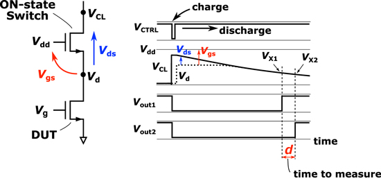
Fig. 2. (Color online) The ON-state switch transistor in the MOSFET selection circuit (left) and voltage waveform of current-to-time converter (right).
Download figure:
Standard image High-resolution imageThird, as the same types of pMOSFET and nMOSFET are used for the inverters, both of the inverter logic threshold voltages are expected to have similar temperature coefficients. Logic threshold voltage VX of an inverter can be expressed as follows. 14)

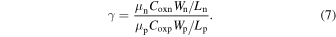
Here Vthp and Vthn are threshold voltages of pMOSFET and nMOSFET, respectively. μp and μn represent mobility for pMOSFET and nMOSFET. Coxp and Coxn are gate oxide capacitances per area. Wp and Wn are the gate widths, and Lp and Ln are the gate lengths. γ here thus represents the driving strength ratio between nMOSFET and pMOSFET. From Eq. (6), we can tune the logic threshold by tuning γ and threshold voltages. Consider the case of tuning the logic threshold by adjusting the pMOSFET threshold voltages of the two inverters. In this case, ΔVX is equal to Vthp2 − Vthp1. Different threshold voltages can be obtained by gate length modulation for example. Threshold voltage typically has a sensitivity of 1–2 mV K−1 against temperature. 14) Assuming both the threshold voltages change by the same amount with a change in temperature, we expect a stable ΔVX over a wide range of temperatures. It should be noted that there are second-order dependencies that may cause some deviation. Figure 3 shows the simulated threshold voltage difference against temperature. The amount of fluctuation for (VX1 − VX2) across a temperature range of 100 °C under five different process corners of "TT", "SF", "FS", "SS" and "FF" is plotted in the figure. We observe negligible fluctuation of (VX1 − VX2) across the temperature range. Thus, we find the second-order effects to be small in the target process.
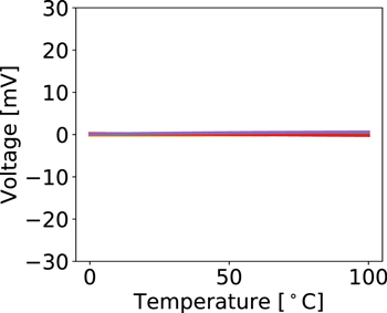
Fig. 3. (Color online) Deviation of logic threshold different at different temperatures and different process corners.
Download figure:
Standard image High-resolution imageFinally, we also need to make sure that the drain voltage remains constant during the current measurement for accurate characterization of different process parameters such as the subthreshold coefficient and threshold voltage. This can be achieved by setting the two threshold voltages close to each other. As illustrated in Fig. 2, the inverters are designed such that the two threshold voltages of VX1 and VX2 become close to each other and these values are much lower.
2.2. Switch structure
The design of the switch tree is important to maximize DUT current ratio to other leakage current ratios. Putting all the DUT MOSFETs in parallel will cause large gate leakage which can be large in scaled processes. To reduce the number of parallel MOSFETs, we use a tree-based switch structure as shown in Fig. 4. In the structure, the switches are divided into several stages and each stage has several branches. With the stacking of the switches, the source voltage of the intermediate transistors rises resulting in negative Vgs and Vbs values. Negative Vgs and Vbs decrease the leakage current further. For the case of 256 DUT MOSFETs, the ratio between DUT current and other leakage currents is simulated to be 168 for the target process when Vg = 0.2 V.
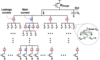
Fig. 4. (Color online) Tree structure of switches to reduce unwanted leakage current.
Download figure:
Standard image High-resolution image2.3. Overall architecture
Figure 5 shows the block diagram of our measurement circuit. Inside the chip, N number of DUT (Device Under Test) MOSFETs are placed and routed along with the switches. First, using serial clock "sclk" and serial data "sdin", the address of the target MOSFET is sent to the chip. The decoder inside the chip decodes the address and generates the signals for the switches to activate the path for the target MOSFET. The "meas" signal is then lowered for some time to allow the output node to charge to Vdd. The "meas" signal is then set to high to let the output node to be discharged by one of the DUT MOSFETs. After the output node is lowered to cross the logic threshold voltages of the inverters, the output signals "out1" and "out2" are then inverted sequentially. The delay difference between the two output signals gives the delay corresponding to the subthreshold current of the target MOSFET. This process is then iterated by selecting the next MOSFET.
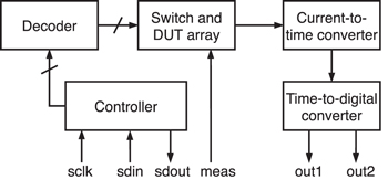
Fig. 5. Block diagram of proposed current measurement flow.
Download figure:
Standard image High-resolution imageA similar complementary test structure can be implemented to measure variations of pMOSFETs. In that case, the output node will be discharged to Vss first, and then the node will be charged by one of the pMOSFETs. In this implementation, we change the address after the completion of each measurement by sending the serial signals which cause some delay. To reduce the test time further, we can implement a counter-on-chip that will increment the address value after the completion of each measurement.
3. Variability characterization methodology
3.1. Subthreshold leakage current
As (VX1 − VX2) is shared among all the DUT devices, and its value is constant across temperature, we can relate the variance of delay to the variance of subthreshold leakage current as follows


3.2. Subthreshold coefficient
The subthreshold coefficient of each MOSFET can be calculated by measuring the current at different gate-source voltages where the MOSFETs operate at weak inversion. Different gate-source voltages can be achieved by tuning Vg in our circuit. Choosing two values of Vg to be Vg1 and Vg2, we obtain the following relationships. 15)
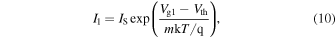
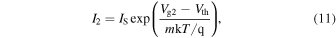


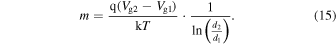
Here, IS is the reverse saturation current, q is the elementary charge, k is the Boltzmann constant, m is the subthreshold coefficient, and T is the absolute temperature. From Eq. (15), we can obtain the value of subthreshold coefficient m for each MOSFET by measuring two delays at two different Vg values.
3.3. Threshold voltage
Accurate characterization of MOSFET threshold voltage variation is not straightforward. Different approaches are used in the literature to define threshold voltage to characterize its variation. 16–19) We can see from Eq. (10) that the threshold voltage Vth and the subthreshold voltage m are closely coupled. These two values cannot be decoupled by tuning the Vgs values only. Thus, for scaled MOSFETs, where the subthreshold coefficient m varies largely, careful interpretation is required for threshold voltage variation. For larger devices, where m variation is negligible, Vth variation can be readily calculated by measuring delays at a constant Vg value using our circuit. 20)


4. Measurement results
4.1. Test chip
We have fabricated a test chip integrating 256 nMOSFETs, the switch tree, the current-to-time converter, and the switch decoder in a 65 nm bulk low-power CMOS process. The layout is designed with a cell-based design flow. Figure 6 shows the chip photograph and layout of our proposed circuit. The area is 0.038 mm2. CL is implemented using MIM capacitor. The value of CL is 10 pF in this test chip which takes an area of 0.0086 mm2. The values of VX1 are 0.29 V, 0.38 V and 0.45 V at Vdd of 0.8 V, 1.0 V and 1.2 V, respectfully. The values of VX1 − VX2 are 40 mV, 50 mV and 70 mV at the three supply voltages.

Fig. 6. (Color online) Chip photograph (left) and overall layout (right).
Download figure:
Standard image High-resolution image4.2. Subthreshold leakage current variation
Figure 7(a) shows the QQ plot of the logarithm of measured delays at Vg = 0.2 V for different temperatures. A linear relationship is observed referring to that leakage current follows a lognormal distribution. This is further confirmed by plotting the histograms of the logarithm of delays for two different temperatures of 0 °C and 100 °C. The histograms are shown in Fig. 7(b). We observe Gaussian-like histograms for the delay logarithms. The variance increases with the lowering of temperature. Figure 8 shows the standard deviation of logarithm of delay against 1/T for three different supply voltages. As predicted by Eq. (17), the standard deviation of the logarithm of delay has a linear relationship against 1/T. We also observe the same linear relationship in Fig. 8, which confirms the validity of the measurement. We also observe that supply voltage change has negligible effect on the distribution.
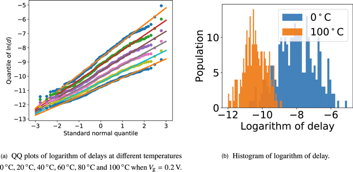
Fig. 7. (Color online) Delay variability at different temperatures.
Download figure:
Standard image High-resolution image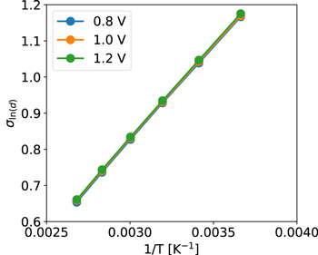
Fig. 8. (Color online) Standard deviation of the logarithm of measured delay against temperature for three different supply voltages of 0.8 V, 1.0 V and 1.2 V when Vg = 0.2 V.
Download figure:
Standard image High-resolution image4.3. Subthreshold coefficient variation
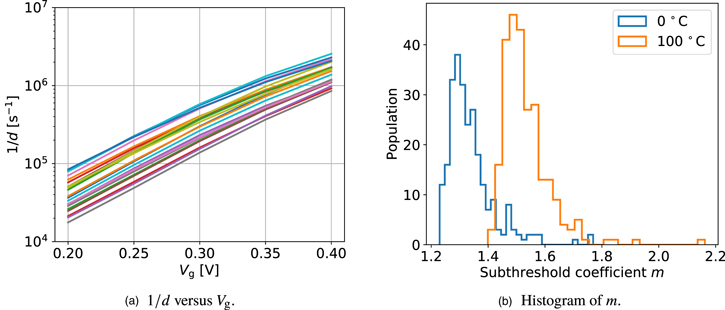
We have measured the delay value for each of the MOSFETs by measuring at different Vg values. Figure 9(a) shows the 1/d over a Vg range from 0.2 V to 0.4 V. We can observe that most of the devices show a linear relationship up to 0.3 V. However, some of the devices show nonlinear relation from 0.35 V which suggests that channel inversion has started for these devices at this point. Next, we have calculated the subthreshold coefficient m for each of the nMOSFETs using delay values at Vg values of 0.2 V and 0.25 V. Figure 9(b) shows the histograms of the calculated m values for two different temperatures of 0 °C and 100 °C. We observe large variation in the m values. This observation is supported by literature reports. 21) However, to the best of our knowledge, our results are the first to demonstrate m distribution for scaled nMOSFETs that are densely placed as found in a digital circuit.
Fig. 9. (Color online) Variability of subthreshold coefficient m.
Download figure:
Standard image High-resolution image
4.4. Threshold voltage
As seen in Fig. 9(b), subthreshold coefficient m is not constant in this process for the minimum sized nMOSFETs. Therefore, Eq. (18) cannot be applied. We need more sophisticated extraction methods to accurately extract threshold voltage variation. Understanding the limitation of Eq. (18), we derive Vth variation assuming that m is constant. We use the median value of m from Fig. 9(b). The extracted standard deviation of Vth is then calculated to be 37 mV at 20 °C temperature. However, we should be careful that this value can be overestimated due to the variation in subthreshold coefficient m.
5. Conclusion
We proposed an on-chip leakage current measurement circuit for statistical modeling. The circuit shares a common current-to-time converter along with a tree-based switching scheme to reduce unwanted leakage currents. Furthermore, a dual interval-based current-to-time conversion reduces errors from comparator delay and switch resistances, as well as eliminates the need for external references. The proposed circuit will help the process engineers measure current variations at different temperatures and bias voltages under a cell-based design where the MOSFETs are densely placed and routed.
Acknowledgments
This work was supported by JSPS KAKENHI 19K20233. This work was also supported through the activities of VDEC, The University of Tokyo, in collaboration with NIHON SYNOPSYS G.K., Cadence Design Systems, and Mentor Graphics.