
Abstract
We report on the formation and optical characteristics of Eu-doped GaN (GaN:Eu)/GaN core–shell nanowires (NWs) grown by organometallic vapor phase epitaxy. A moderate V/III ratio and growth temperature enable the incorporation of Eu3+ ions into the GaN shells on GaN core NWs, resulting in red luminescence at room temperature whose peak intensity is more than 20 times larger than for a GaN:Eu film on planar GaN. The cathodoluminescence characterization corroborates that the observed enhanced Eu luminescence originates from the predominant formation of highly efficient Eu centers in the sidewalls of the GaN:Eu/GaN core–shell NWs.
Export citation and abstract BibTeX RIS
1. Introduction
Recently, there has been a growing demand for the realization of micro-/nano-displays for next-generation display technologies towards advent of a super-smart society. Nowadays, light-emitting diode (LED) technology has been applied to stationary, large and high-definition displays. The miniaturization of display devices has recently been progressing towards portable devices including ultra-small projectors, micro-displays or head-up displays. In the near future, such portable displays are expected to evolve to flexible and wearable devices including retinal projection displays. In order to realize this type of flexible and wearable display devices, it is necessary to achieve three primary color light emission on the same platform and the further miniaturization of pixel size. However, when the dimensions of μ-LEDs are reduced to below ∼100 μm by using the conventional top-down approaches such as dry or wet etching processes, their sidewalls suffer from damages induced by the fabrication processes, leading to the introduction of non-radiative recombination associated with imperfections of the sidewalls, and resulting in a lowering of the internal quantum efficiency due to the carriers with long diffusion lengths reaching the sidewalls.
Rare-earth (RE) doped semiconductors have recently emerged as promising materials for highly efficient electroluminescent devices due to their advantageous optical characteristics of sharp luminescence with an ultra-high wavelength stability against operating temperature due to the intra-4f shell transitions of RE ions. This material can be easily obtained by simply doping semiconductors with RE ions, and hence can be used to realize light emitters with a high color purity. Our group has demonstrated red LEDs based on GaN doped with Eu (GaN:Eu) 1) with an optical output power exceeding 1 mW at 20 mA, 2) which is a respectable value for practical applications. Furthermore, a monolithic vertically stacked GaN-based full-color LEDs using GaN:Eu as the red component has been demonstrated, 3) which paves the way towards the development of μ-LED displays. Additionally, our latest study has revealed that Eu3+ ions are very efficient at trapping injected carriers resulting in shorter carrier diffusion lengths (∼100 nm) and significantly suppresses the decrease in quantum efficiency, realizing values of ∼90% of the maximum value for the sizes as small as 3 μm. 4,5) However, there still remain limitations associated with damaged sidewalls when the chip size of such GaN:Eu-based μ-LEDs would further decrease to the submicron sizes.
Semiconductor nanowire (NW)-based light emitters have been exploited as ultra-small, highly efficient coherent light sources and have at least one dimension comparable to the diffraction limit of its emission wavelengths. NWs are typically grown by bottom-up approaches, including vapor-liquid-solid method or selective growth techniques, which provides the opportunity for their explicit control of their composition and dimension during growth. Bottom-up growth technologies have enabled the production of complex superlattices structures for diverging applications in Si photonics, biological/environmental sensing and flexible/wearable display technologies. Above all, GaN-based NWs 6–13) have attracted potential interest for next-generation displays such as retinal projection glasses and contact lenses as the NW architecture could drastically miniaturize pixel sizes. Furthermore, NW structures can be transferred to flexible membranes 14–16) such as polydimethylsiloxane, which could realize flexible optoelectronic nanodevices based on inorganic semiconductors. So far, there have been several demonstrations of NW-based photonic devices including light emitters such as nanolasers, 17) photonic-crystal-(PhC)-based lasers, 18,19) or LEDs, 20–24) photovoltaics, 25) photodetectors, 26) and temperature sensors. 27) In addition, the use of NW architecture enables the growth of GaN:Eu with a higher Eu concentration than the film configuration due to the inherent strain relaxation 28) induced by its finite lateral dimensionality. 9) Therefore, it would be beneficial to improve the output power for NW-based light emitters where GaN:Eu is used as the active component.
In this paper, we report on the formation and optical characteristics of GaN:Eu/GaN core–shell NWs grown by organometallic vapor phase epitaxy (OMVPE). In the first part, the growth conditions of GaN:Eu shells on GaN core NWs are optimized in order to maximize Eu luminescence by changing the V/III ratio and growth temperature. Subsequently, the optical characteristics of Eu luminescence in the GaN:Eu shells are studied and compared with conventional GaN:Eu films grown with the same growth conditions as the NW configuration. Finally, cathodoluminescence (CL) characterization of the GaN:Eu/GaN core–shell NW is performed to corroborate the centers responsible for Eu luminescence in the GaN:Eu/GaN core–shell NWs sidewall.
2. Experimental methods
All samples were grown by OMVPE (Taiyo Nippon Sanso SR-2000). Trimethylgallium (TMGa), ammonia (NH3) and bis(n-propyl-tetramethylcyclopentadienyl)-europium [Eu(Cppm 2)] were used as Ga, N and Eu precursors, respectively. The bubbler of Eu(Cppm 2) was completely covered with a mantle heater and the temperature was set at 145 °C. The formation process was initiated with the growth of ∼5 μm thick undoped-GaN (ud-GaN) template on sapphire (0001) substrates. Next, a 20 nm thick silicon dioxide (SiO2) was deposited on the GaN template as a growth mask layer, and then patterned with a triangular array of apertures with an average opening diameter of 200 nm and a pitch of 1347 nm by an electron beam (EB) lithography (Elionix, ELS-G125FI). Subsequently, reactive ion etching (RIE, Samco, RIE-10NOU) was performed to fabricate the SiO2 patterned mask. After cleaning the patterned templates, they were loaded immediately into the reactor, and hexagonal GaN core NWs were grown at 1090 °C with an average height and diagonal length of 588 and 427 nm, respectively, by simultaneously supplying TMGa and NH3 at a V/III ratio of 39 with flow rates of 31.7 and 1250 μmol min−1, respectively [Figs. 1(a) and 1(b)]. A H2/N2 carrier gas mixture of 0.57 was maintained at a pressure of 10 kPa. The growth duration of the GaN core NWs was 4 min. A filling process 8) was applied before the growth of the core NWs to improve the uniformity of the initial NWs growth. In this growth step, TMGa and NH3 were supplied simultaneously at a V/III ratio of 1734 with flow rates of 22.4 μmol min−1 and 38.8 mmol min−1, respectively, under a pure H2 carrier gas for 45 seconds at a pressure of 20 kPa. Finally, we grew GaN:Eu shell structures by doping Eu into GaN, as illustrated in Fig. 1(c). The TMGa and Eu(Cppm 2) molar flow during the growth of GaN:Eu shells were kept constant at 25.6 and 1.86 μmol min−1, respectively, under a pure H2 carrier gas for 5 min at a pressure of 10 kPa. The flow rate of NH3 was varied in order to change the V/III ratio during the growth of the shell layers. The structural characterization of the NWs was carried out by scanning electron microscope (SEM, Hitachi High-Tech, SU-9000). The optical characterization of an ensemble of NWs was performed using a conventional micro-photoluminescence (PL) setup equipped with a Si photodiode array (Teledyne Princeton Instruments, PIXIS 1300BeXcelon) and a 50 cm monochromator (Teledyne Princeton Instruments, SpectraPro HRS-500). The spectral resolution was approximately 0.02 nm. The PL spectra at low temperature were collected by mounting the samples in an ultra-low-vibration cryostat (Montana Instruments, Cryostat S50). A He–Cd laser (325 nm, Kimmon Koha, IK3101R-D) was used as an excitation source for the PL characterization. Luminescence mapping of a single NW was performed by CL spectroscopy from the top of the NWs by using a field-emission SEM (JEOL JSM-6500F) equipped with a CL measurement unit. This was achieved by collecting CL luminescence induced by a focused EB using an ellipsoidal mirror and detected through an optical fiber bundle and a 32 cm spectrometer (HORIBA, TRIAX320) with a spectral resolution of 1.32 nm. All CL images were taken with a 1 mm slit width to obtain a larger CL signal.
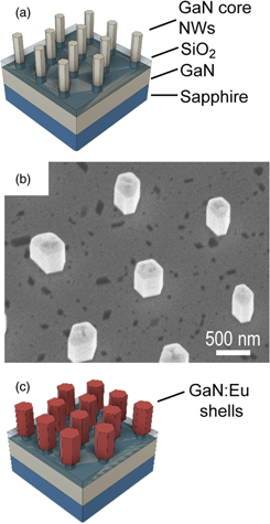
Fig. 1. (Color online) (a) Schematics and (b) SEM image of GaN core NWs and (c) schematics of GaN:Eu/GaN core–shell NWs on patterned GaN templates.
Download figure:
Standard image High-resolution image3. Results and discussions
The geometry of the GaN:Eu shell largely depends on several growth parameters including growth temperature, reactor pressure, growth rate and V/III ratio. In this study, the structural and optical characterization of GaN:Eu/GaN core–shell NWs are performed by changing two growth parameters, the V/III ratio and growth temperature, which have a significant effects on the growth of NWs. In general, a high V/III ratio during the growth of ud-GaN NWs allows to increase the growth rate along the 〈1–100〉 directions, and the semi-polar tapered facets ({1–102} and {1–101}) tend to become dominant. 7) Figures 2(a)–2(d) show SEM images of GaN:Eu/GaN core–shell NWs whose shell layers are grown at 1050 °C with V/III ratios of 350, 700, 1400 and 2800, respectively, realized by changing the NH3 molar flow under the same TMGa and Eu(Cppm 2) molar flow. From the dimensions of core–shell NWs summarized in Table I, the growth of the GaN:Eu layer takes place along both [0001] and 〈1–100〉 directions, suggesting that the GaN:Eu layer is formed in a core–shell manner. In contrast, NWs without Eu doping under equivalent growth conditions exhibit a hexagonal pyramid-shaped structure without the {1–100} sidewalls. This is likely a result of an antisurfactant effect induced by Eu doping at the NW sidewalls. A similar phenomenon has been reported for Si doping into GaN NWs, which enhances the growth along the [0001] direction. 29) The height and diagonal length at the bottom part of the NWs shows a gradual increase, but the sidewall tends to taper with increasing V/III ratio due to a decreased diffusion length of Ga adatoms. Since the growth along the 〈1–100〉 directions takes place by migrating Ga adatoms from the SiO2 masked region onto the sidewalls, a small diffusion length of Ga adatoms increases the likelihood of growth of the bottom part of the sidewalls. The height of the NWs decreases and the shape becomes more truncated when the V/III ratio is 2800, resulting in a decreased volume of the GaN:Eu shell layers. Figure 2(e) shows the PL spectra at room temperature (RT) of the GaN:Eu/GaN core–shell NWs with different V/III ratio. Luminescence from Eu ions doped in GaN is observed in the vicinity of ∼621 nm in all core–shell NWs, while no Eu luminescence is observed from the core NWs. It is noted that a broad yellow luminescence spectrum, as well as band-edge light emission from GaN, is observable. The PL intensity of Eu luminescence becomes stronger for increasing V/III ratio from 350 to 1400 but the PL intensity decreases when the V/III ratio becomes 2800. This trend shows a moderate agreement with the average total volume of the GaN:Eu shell layers which can be derived from Table I. Therefore, a moderate V/III ratio of 1400 is necessary to maximize the PL intensity of Eu luminescence in the GaN:Eu shells.
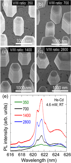
Fig. 2. (Color online) SEM images of GaN:Eu/GaN core–shell NWs grown at V/III ratios of (a) 350, (b) 700, (c) 1400 and (d) 2800. (e) RT PL spectra of GaN:Eu/GaN core–shell NWs grown at V/III ratios of 350, 700, 1400 and 2800.
Download figure:
Standard image High-resolution imageTable I. Average diagonal length of the top and bottom parts and height of the GaN:Eu/GaN core–shell NWs versus V/III ratios.
| V/III ratio | Average diagonal length (NW top) | Average diagonal length (NW bottom) | Average NW height |
|---|---|---|---|
| (nm) | (nm) | (nm) | |
| 350 | 673 | 673 | 1576 |
| 700 | 769 | 769 | 1592 |
| 1400 | 654 | 860 | 1803 |
| 2800 | 523 | 846 | 907 |
| Core only | 427 | 427 | 588 |
Figures 3(a)–3(d) show the SEM images of GaN:Eu/GaN core–shell NWs with growth temperatures of 990 °C, 1020 °C, 1050 °C, and 1080 °C, respectively. The NW height tends to increase with the growth temperature (<1050 °C) as summarized in Table II, which is due to an increasing diffusion length of Ga adatoms. However, the NW height decreases when the growth temperature exceeds 1050 °C due to enhanced desorption of Ga adatoms. Figure 3(e) shows PL spectra at RT of the GaN:Eu/GaN core–shell NWs with different growth temperatures, showing that a moderate growth temperature (from 1020 °C to 1050 °C, specifically) is essential to maximize the PL intensity of Eu luminescence in the GaN:Eu shell. These results suggest that a moderate V/III ratio and growth temperature are required for optimal Eu incorporation into GaN:Eu/GaN core–shell NWs.

Fig. 3. (Color online) SEM images of GaN:Eu/GaN core-shell NWs grown at growth temperature of (a) 990 °C, (b) 1020 °C, (c) 1050 °C and (d) 1080 °C. (e) RT PL spectra of GaN:Eu/GaN core–shell NWs grown at growth temperature of 990 °C, 1020 °C, 1050 °C and 1080 °C.
Download figure:
Standard image High-resolution imageTable II. Average diagonal length of the top and bottom parts and height of the GaN:Eu/GaN core–shell NWs versus growth temperature.
| Growth temperature (°C) | Average diagonal length (NW top) | Average diagonal length (NW bottom) | Average NW height |
|---|---|---|---|
| (nm) | (nm) | (nm) | |
| 990 | 502 | 828 | 1074 |
| 1020 | 619 | 935 | 1219 |
| 1050 | 654 | 860 | 1803 |
| 1080 | 293 | 569 | 1308 |
μ-PL measurements of both GaN:Eu/GaN core–shell NWs (V/III ratio of 1400 and growth temperature of 1050 °C) and GaN:Eu films grown with equivalent growth conditions are performed at low temperature in order to clarify the detailed optical characteristics of Eu3+ ions in the GaN:Eu shells. Figure 4 shows PL spectra at 10 K demonstrating a more than 20 times enhancement of the peak intensity from Eu3+ luminescence in GaN:Eu shells compared to that of the film configuration. Furthermore, we note here the considerable difference of spectral shape; while the film has more peaks and broader emission spectrum due to the occurrence of multiple incorporation centers, the NWs shows a much sharper and cleaner spectrum with less peaks. This implies that there are fewer types of incorporation centers, and better-defined peaks due to strain relaxation. The most intense peak of the GaN:Eu/GaN core–shell NWs is located at different wavelength of approximately 620.8 nm as indicated by the red line and that of the GaN:Eu films at approximately 622 nm. The Eu luminescence peak at 620.8 nm (1.997 eV) originates from a luminescence center that is designated OMVPE7, 30,31) and is well-known to be the center with the highest excitation efficiency especially under current injection. 32,33) The use of NW configuration results in enhanced PL intensities form the combination of the preferential formation of the high-efficient Eu luminescence center and an improvement of light extraction efficiency. It is noted that the peak wavelength of the OMVPE7 for GaN:Eu/GaN core–shell NWs is shorter than the film samples, due to inherent strain relaxation 28) in the NW configuration as compared to the film. Indeed, our previous report has revealed that a red shift in the emission peak position of OMVPE7 is observed when the GaN host material suffers from in-plane compressive strain by using AlGaN/GaN super lattices. 34) These results suggest that the use of a NW configuration in a LED structure based on Eu-doped GaN would be advantageous for the realization of nano light emitters under current injection, in conjunction with the other side effects of increasing the concentration of optically active Eu3+ ions and an improvement of the light extraction efficiency. 35)
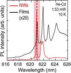
Fig. 4. (Color online) PL spectra at 10 K of GaN:Eu/GaN core–shell NWs and GaN:Eu films on planar GaN templates grown under the equivalent growth conditions.
Download figure:
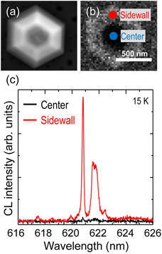
Standard image High-resolution imageFinally, SEM and CL intensity mapping of a single GaN:Eu/GaN core–shell NW is performed at 15 K. Figure 5(a) shows a top-view SEM image of a NW. Figure 5(b) shows a CL intensity mapping taken at a center wavelength of 621 nm of the same area. CL spectra taken at the center and sidewall of the NW are shown in Fig. 5(c). Eu luminescence is observed from the sidewalls of the NW, while almost no luminescence is observed from the center of the NW. Due to the limited spectral resolution for the CL detection, the imaging map cannot distinguish different luminescent centers, and includes contributions from all centers. However, the CL characterization result corroborates that obtained Eu luminescent center of the NWs originates predominantly from Eu3+ ions doped in the sidewall of the GaN:Eu/GaN core–shell NWs and demonstrates a difference in Eu adsorption on the top and sidewall of the NWs. A detailed cross-sectional CL characterization is required to precisely evaluate the mapping of the Eu concentration in the NWs, and will be discussed in future publications.
Fig. 5. (Color online) (a) Top view SEM and (b) CL mapping images of GaN:Eu/GaN core–shell NWs. (c) CL spectra of the center and sidewall of the GaN:Eu/GaN core–shell NWs.
Download figure:
Standard image High-resolution image
4. Conclusions
We report on the growth and optical characteristics of GaN:Eu/GaN core–shell NWs grown by OMVPE. GaN:Eu shell layers are grown on GaN core NWs formed on patterned GaN templates. Optimization of the growth conditions of the GaN:Eu shells elucidates that moderate V/III ratio and growth temperature enables Eu incorporation in GaN:Eu/GaN core–shell NWs with the highest PL intensity from Eu3+ ions in the GaN:Eu shells. This growth optimization results in red luminescence at RT with a PL intensity of more than 20 times stronger than GaN:Eu films grown on planar GaN using equivalent growth conditions. The CL characterization corroborates that the observed enhanced Eu luminescence originate from Eu3+ ions in a high efficiency center, that are predominantly doped in the sidewalls of the NWs. These results indicate the feasibility of NW-based light emitters based on GaN:Eu, and would pave the way for the realization of next-generation ultra-small high-resolution displays.
Acknowledgments
This work was partly supported by Grant-in-Aid for Scientific Research (B) (Grant No. 19H02573), Grant-in-Aid for Specially Promoted Research (Grant No. 18H05212) of the Japan Society for the Promotion of Science, Nanotechnology Platform (Grant No. JPMXP09F21OS0021 and JPMXP09S21OS0013) of the Ministry of Education, Culture, Sports, Science and Technology (MEXT), the Murata Science Foundation, the Samco Foundation and the Canon Foundation.