
Abstract
ScAlN films are currently being investigated for their potential use in surface acoustic wave (SAW) devices for next-generation mobile networks because of their high piezoelectricity. This paper describes the numerical simulation of SAW propagation in c-axis-tilted ScAlN films on silicon substrates and a fabrication technique for preparing c-axis-tilted ScAlN films on silicon substrates. The electromechanical coupling coefficient K2 of SAW propagating in the ScAlN film/silicon substrate increased due to the c-axis tilt angle. The maximum K2 value is approximately 3.90%. This value is 2.6 times the maximum K2 value of the c-axis-oriented ScAlN film/silicon substrate structure. The c-axis-tilted ScAlN films with an Sc concentration of 40% were prepared on a silicon substrate via RF magnetron sputtering based on the self-shadowing effect, and the maximum c-axis tilt angle was 57.4°. These results indicate that this device structure has the potential for SAW device applications with well-established micromachining technology derived from silicon substrates.
Export citation and abstract BibTeX RIS
1. Introduction
Surface acoustic wave (SAW) devices with a high frequency (gigahertz range), high electromechanical coupling coefficient K2, and high Q factor are required for filters and duplexers in smartphones. 1–3) In particular, high K2 values contribute to the wide bandwidth of SAW devices. The piezoelectric film/high-velocity substrate structure offers great advantages in the fabrication of SAW devices with a high electromechanical coupling coefficient K2. SAW devices comprising piezoelectric films, such as AlN, ZnO, LiNbO3, and LiTaO3, on diamond substrates with the highest bulk acoustic wave (BAW) velocities have been studied previously. 4,5) Akiyama et al. recently found ScAlN to be an important candidate for the piezoelectric film layer. The piezoelectric coefficient d33 of ScAlN increases with the Sc concentration, and the d33 value of ScAlN with an Sc concentration of 40% is approximately five times that of AlN. 6–8) Furthermore, recent studies have shown the appearance of ferroelectricity in ScAlN films. 9–12) Therefore, ScAlN films are currently being investigated to explore their potential for use in SAW devices for next-generation mobile networks. 13–20) In particular, SAW devices based on ScAlN film/high velocity substrate (e.g. diamond and SiC) structures were reported to have a maximum K2 of 5.48%, which is a much higher K2 value than AlN-based SAW devices. 21–23)
Although diamond and SiC provide high K2 values, SAW devices that use them as substrates are rarely put into practical use. This is because the diamond substrate fabrication technology is currently in the research phase, which makes these substrates very expensive. 24,25) The SiC substrate fabrication process is well established compared to that of diamond substrates. However, SiC substrates have a cost disadvantage compared to quartz and LiNbO3, which are currently used in SAW devices. It is difficult to fabricate SAW devices using high-velocity substrates for practical use.
Because the phase velocity of silicon is lower than those of diamond and SiC, the K2 value decreases in SAW devices that use silicon substrates. 26) However, silicon is known as an inexpensive substrate. In addition, silicon substrates provide well-established micromachining technology, which makes SAW devices based on silicon substrates compatible with various micromechanical structures. 27–30) Therefore, SAW devices using ScAlN film/silicon substrate structures are attractive if the K2 value of this SAW device increases. In a previous study, we showed that the K2 value of SAW propagating in wurtzite films, including ScAlN films on sapphire substrates, increased with the c-axis tilt of the wurtzite. 31) SAW devices using c-axis-tilted ScAlN film/silicon substrate structures may exhibit high K2 values and have significant potential for practical applications.
Sputtering deposition is widely used to prepare ScAlN films. A highly c-axis-oriented ScAlN polycrystalline film can be prepared by sputtering deposition. 6–15,21,22,32) A deposition method capable of preparing a c-axis-tilted film is required for the fabrication of c-axis-tilted ScAlN film/silicon substrate structures. Highly tilted polycrystalline films can be tailored by the glancing angle deposition (GLAD) technique, which is based on the self-shadowing effect. 33–36) In this effect, the crystal orientation of the polycrystalline film grown on the substrate depends on the angle of the particle flux to the substrate. 33) Sputtering deposition using self-shadowing effects has recently been shown to be effective in preparing c-axis-tilted wurtzite films. 37) Therefore, it is highly possible that c-axis-tilted ScAlN films can be prepared on silicon substrates using this deposition method. Furthermore, the film growth is affected not only by the particle flux to the substrate, but also by the atomic arrangement of the substrates. 38) In addition, it has been reported that ScAlN films on diamond-like carbon do not crystallize when the Sc concentration exceeds 35%. 39) This result is an important problem in SAW device applications, because the piezoelectricity of ScAlN films is maximized at an Sc concentration of 40%. 6–8) We predicted similar results for ScAlN films on silicon substrates because silicon has the same cubic structure as diamond-like carbon. A method for crystallizing ScAlN films with an Sc concentration of 40% is required.
In this study, to investigate whether a c-axis-tilted ScAlN film/silicon substrate structure has a high K2 value, we performed a theoretical analysis of SAW propagation on a c-axis-tilted ScAlN film/silicon substrate structure and a method for preparing a c-axis-tilted ScAlN film on a silicon substrate. 40) The K2 values of Rayleigh-mode and Sezawa-mode SAW propagating in the ScAlN film/silicon substrate structure are calculated in detail for two types of interdigital transducer (IDT) arrangements, and the effect of c-axis tilt on the increase in K2 is discussed. In addition, we considered the crystal growth method for highly c-axis-tilted ScAlN films with Sc concentrations of 30% or 40% on a silicon substrate by the sputtering method using self-shadowing effects. The effects of the SiO2 thin film buffer layer, which is important for obtaining this structure using ScAlN films with an Sc concentration of 40%, are discussed.
2. Analysis of SAW propagation in c-axis-tilted ScAlN film/silicon substrate structures
2.1. Electromechanical coupling coefficient K2
The propagation characteristics of SAWs were theoretically analyzed to investigate the effect of the c-axis tilt angle on the electromechanical coupling coefficient K2 of SAW propagating in the ScAlN film/silicon substrate structure. Figure 1 shows two types of theoretical analysis models for SAW propagation in a ScAlN film/silicon substrate layered structure. The IDT electrodes were placed on the surface of the ScAlN films in both models. The boundary between the ScAlN films and silicon substrates is electrically open in the A structure and electrically short-circuited in the B structure. The piezoelectric coefficients, eij , and elastic constants, cij , calculated using density function theory for a single-crystal ScAlN were used in the ScAlN layer of these models. 41) The relative permittivity, εij , of the ScAlN layer was set to 1.9 times the relative permittivity of the single-crystal AlN 42) to consider the experimental value. The density of the ScAN layer is an experimental value (3638 kg m−3) measured using Archimedes' method. The material constants of silicon substrates are used the values reported as a single-crystal silicon. 43) We analyzed SAW K2 values using the Campbell and Jones' method 44) when normalized ScAlN film thickness H/λ and the c-axis tilt angle χ of the ScAlN film were varied for these structures. The effect of the piezoelectric constant e33, which is largest value among the piezoelectric constants of ScAlN, on the Rayleigh-mode SAW excitation is maximized when the SAW propagates in the c-axis tilt direction. The particle displacement for the shear horizontal (SH) component increases with the increase in angle between the SAW propagation direction and the c-axis tilt direction, which reduces the effect of the piezoelectric constant e33 on Rayleigh-mode SAW excitation. Therefore, The Euler angle of the ScAlN films and silicon substrates in these structures is set to (0°, χ, 90°) and (0°, 0°, 0°), respectively. The K2 value is calculated using the equation K2 = 2(vf − vm)/vf, where vf and vm are the phase velocities in an electrically open surface and electrically short-circuited surface, respectively.
Fig. 1. (Color online) Theoretical analysis model for SAW propagation in air/Sc0.4Al0.6N film/silicon substrate structure. The IDT electrodes were placed on the surface of the ScAlN films in both models. The boundary between the ScAlN films and silicon substrates is electrically open in the A structure and electrically short-circuited in the B structure.
Download figure:
Standard image High-resolution imageFigures 2(a) and 2(b) show phase velocities of the Rayleigh-mode SAW in an electrically open surface for A and B structure, respectively. The horizontal and vertical axes present H/λ and the c-axis tilt angle χ, respectively. The phase velocity depends largely on H/λ because SAW velocities in silicon are larger than those in ScAlN. In addition, phase velocities depend on the c-axis tilt angle χ. This is because the phase velocity of the quasi-shear wave in ScAlN depends on the c-axis tilt angle χ and affects the SAW phase velocity. The phase velocity of the quasi-shear wave in ScAlN decreases until the c-axis tilt angle χ reaches approximately 45° and then increases until it reaches 90°. Figures 3(a) and 3(b) show the K2 value of the Rayleigh-mode SAW for A and B structure, respectively. The horizontal and vertical axes present H/λ and the c-axis tilt angle χ, respectively. The maximum K2 values at χ = 0° are 0.31% (H/λ = 0.10) and 1.52% (H/λ = 0.04) for the A and B structures, respectively. χ = 0° represents the c-axis-oriented ScAlN film/silicon substrate structure. Conversely, the maximum K2 value of SAW propagating in the c-axis-tilted ScAlN film/silicon substrate structure is 3.88% (H/λ = 0.53 and χ = 56°) and 3.90% (H/λ = 0.51 and χ = 46°) for the A and B structures, respectively. The K2 value increased significantly with the c-axis tilt angle χ. The phase velocities under the analysis conditions where the maximum K2 values were obtained for the A and B structures were 4256 m s−1 and 4175 m s−1, respectively. Figures 4(a) and 4(b) show phase velocities of the Sezawa-mode SAW in an electrically open surface for A and B structure, respectively. The phase velocities of the Sezawa-mode SAW is higher than those of the Rayleigh-mode SAW and depend on H/λ and the c-axis tilt angle χ similar to those of Rayleigh-mode SAW. Figures 5(a) and 5(b) show the K2 value of the Sezawa-mode SAW. The maximum K2 values of the Sezawa-mode SAW are 2.48% (H/λ = 0.61 and χ = 0°) and 2.61% (H/λ = 0.58 and χ = 0°) for the A and B structures, respectively. The phase velocities under the analysis conditions where the maximum K2 values were obtained were 5584 m s−1 and 5601 m s−1 for the A and B structures, respectively. There was no effect of ScAlN film c-axis tilt on the increase in the K2 value, because the maximum K2 value was obtained at χ = 0° in both structures. These results indicate that the c-axis-tilted ScAlN film/silicon substrate layered structure is suitable for Rayleigh-mode SAW devices.

Fig. 2. (Color online) Phase velocities of Rayleigh-mode SAW for (a) A and (b) B structure. The horizontal and vertical axes show the normalized ScAlN film thickness H/λ and c-axis tilt angle χ, respectively. The color bar range is from 4000 to 5000 m s−1.
Download figure:
Standard image High-resolution image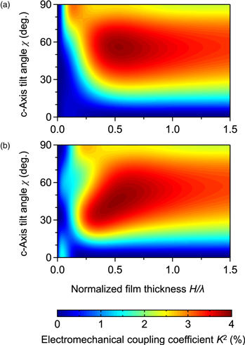
Fig. 3. (Color online) K2 value of the Rayleigh-mode SAW for (a) A and (b) B structure. The horizontal and vertical axes show the normalized ScAlN film thickness H/λ and c-axis tilt angle χ, respectively. The maximum K2 values of the SAW are 3.88% (H/λ = 0.53 and χ = 56°) and 3.90% (H/λ = 0.51 and χ = 46°) for the A and B structures, respectively.
Download figure:
Standard image High-resolution image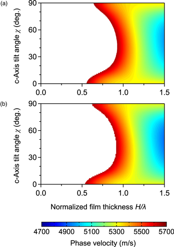
Fig. 4. (Color online) Phase velocities of Sezawa-mode SAW for (a) A and (b) B structure. The horizontal and vertical axes show the normalized ScAlN film thickness H/λ and c-axis tilt angle χ, respectively. The color bar range is from 4700 to 5700 m s−1.
Download figure:
Standard image High-resolution image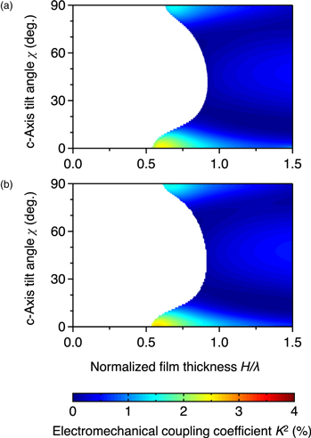
Fig. 5. (Color online) K2 value of the Sezawa-mode SAW. The horizontal and vertical axes show the normalized ScAlN film thickness H/λ and c-axis tilt angle χ, respectively. The maximum K2 values are 2.48% (H/λ = 0.61 and χ = 0°) and 2.61% (H/λ = 0.58 and χ = 0°) for A and B structures, respectively.
Download figure:
Standard image High-resolution imageThe K2 value of the Rayleigh-mode SAW increased with the c-axis tilt angle χ because of the increased excitation of bulk shear waves. Figure 6 illustrates the calculated electromechanical coupling coefficient of the ScAlN quasi-longitudinal wave k'L 2 and the quasi-shear wave k'S 2, as functions of the c-axis tilt angle χ; the propagation direction is x1. The angle χ is the angle from the x3 direction. The k'L 2 and k'S 2 values increase with χ and are maximized at 90° and 58°, respectively. These results show the same tendency as the angle χ dependence on the K2 value of the Rayleigh-mode SAW, as shown in Fig. 3. In particular, the angle χ at the maximum K2 value of the Rayleigh-mode SAW in the A structure is in good agreement with the angle χ at the maximum value of k'S 2 value. In addition, IDT electrodes mainly form an electric field in the x1 direction in the A structure, as shown in Fig. 1. Therefore, the angle χ at the maximum K2 value in the A structure is influenced by the excitation of the quasi-shear wave propagating in the x1 direction. However, the angle χ at the maximum K2 value in the B structure is 46°, which is lower than that in the A structure. This is because an electric field in the x3 direction is generated from the IDT electrodes owing to the short-circuited boundary between the ScAlN films and silicon substrates. The k'S 2 value of the quasi-shear wave propagating in the x3 direction is maximized when χ is approximately 32°. Therefore, the excitation and propagation of SAWs in the B structure are influenced by these conditions. Accordingly, the excitation of quasi-shear waves affects the Rayleigh-mode SAW.
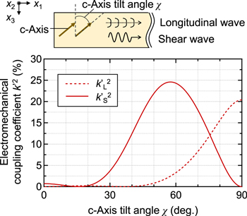
Fig. 6. (Color online) Theoretical electromechanical coupling coefficient of the quasi-longitudinal wave k'L 2 (dashed line) and the quasi-shear wave k'S 2 (solid line) as functions of the c-axis tilt angle χ. k'L 2 and k'S 2 are maximized at χ = 90° and 58°, respectively.
Download figure:
Standard image High-resolution image2.2. Particle displacements
Particle displacements of the Rayleigh-mode SAW in periodic IDT/ScAlN film/silicon substrate structures were simulated using two-dimensional finite element analysis (2D-FEM) to consider the increase in the K2 value in terms of SAW propagation characteristics. The simulation was performed using Femtet® software (Murata Software Co., Ltd.). In the analysis, the wavelength λ was 8 μm, the thickness of the substrate was 10λ, and a perfectly matching layer of 3λ was constructed on the bottom of the substrate. The mechanical and dielectric losses of each layer were not considered. Particle displacement analysis was performed on the structures in which the maximum K2 was obtained in the A and B structures, as shown in Fig. 3. Specifically, the ScAlN film (H/λ = 0.53 and χ = 56°)/silicon substrate layered structure with K2 = 3.88% in the A structure and the ScAlN film (H/λ = 0.51 and χ = 46°)/silicon substrate layered structure with K2 = 3.90% in the B structure were analyzed. To compare these results, we analyzed the structure with the maximum K2 value at χ = 0°, which is the ScAlN film (H/λ = 0.04)/silicon substrate layered structure with K2 = 1.52% in the B structure. Figure 7 demonstrates the particle displacement contours for the longitudinal (L) and shear vertical (SV) components. The displacements were normalized using the maximum value of the SV component in each structure. In all the structures, the SV component had a larger particle displacement than the L component. The area where the SV component shows a large particle displacement in Figs. 7(b) and 7(c) is larger than that in Fig. 7(a). The SV component is mostly concentrated in the ScAlN films, which is approximately half a wavelength thick. The c-axis-tilted ScAlN films/silicon substrate structure provides relatively less energy leakage to the substrate layer, and thus offers efficient SAW propagation and a larger K2 value.
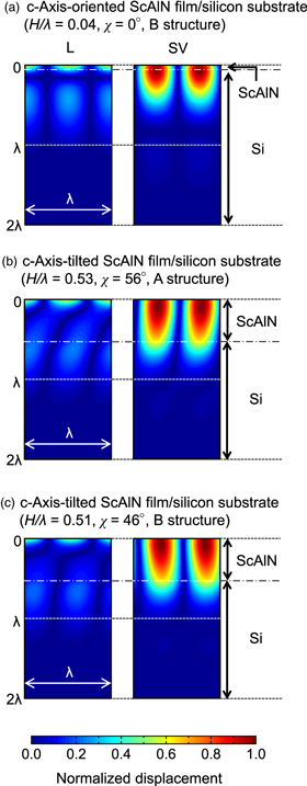
Fig. 7. (Color online) Displacement contours of the Rayleigh-mode SAW in (a) a c-axis-oriented ScAlN film/silicon substrate (H/λ = 0.04, χ = 0°, B structure), (b) a c-axis-tilted ScAlN film/silicon substrate (H/λ = 0.53, χ = 56°, A structure), and (c) a c-axis-tilted ScAlN film/silicon substrate (H/λ = 0.51, χ = 46°, B structure). The particle displacement contours of the longitudinal (L) and shear vertical (SV) components in the region from the ScAlN film surface to a depth of two wavelengths are shown.
Download figure:
Standard image High-resolution imageIn addition, particle displacements of the Sezawa-mode SAW in periodic IDT/ScAlN film/silicon substrate structures were simulated. Figure 8 demonstrates the particle displacement contours for the L and SV components of the Sezawa-mode SAW. The L and SV components are concentrated in the film layer for the ScAlN film (H/λ = 0.61 and χ = 0°)/silicon substrate layered structure with K2 = 2.48% in the A structure, as shown in Fig. 8(a). The same is true for the ScAlN film (H/λ = 0.58 and χ = 0°)/silicon substrate layered structure with K2 = 2.61% in the B structure. However, the particle displacements for the L and SV components leak into the silicon substrate due to the increase in the c-axis tilt angle χ, as shown in Fig. 8(b). The K2 value of the Sezawa-mode SAW propagating in the ScAlN film (H/λ = 0.91 and χ = 56°)/silicon substrate layered structure is 0.09%. Whereas the K2 value of the Rayleigh-mode SAW propagating in the A structure is maximized at the χ = 56°, the K2 value of the Sezawa-mode SAW is significantly decreased due to the relatively large energy leakage to the substrate. In short, there was no effect of ScAlN film c-axis tilt on the increase in the K2 value of Swzawa-mode SAW.
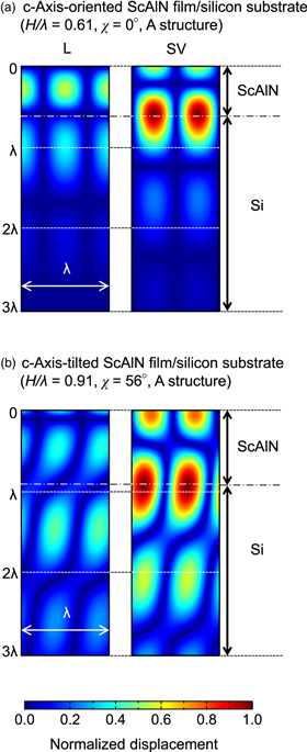
Fig. 8. (Color online) Displacement contours of the Sezawa-mode SAW in (a) a c-axis-oriented ScAlN film/silicon substrate (H/λ = 0.61, χ = 0°, A structure) and (b) a c-axis-tilted ScAlN film/silicon substrate (H/λ = 0.91, χ = 56°, A structure). The particle displacement contours of the longitudinal (L) and shear vertical (SV) components in the region from the ScAlN film surface to a depth of three wavelengths are shown.
Download figure:
Standard image High-resolution image3. Fabrication of c-Axis-tilted ScAlN film/silicon substrate structure
3.1. c-Axis-tilted ScAlN films with Sc concentration of 30% grown on silicon substrates
To obtain a high electromechanical coupling coefficient K2 in SAW propagating in the ScAlN film/silicon substrate structure, it is crucial to prepare c-axis-tilted ScAlN films on silicon substrates. GLAD is a deposition technique, based on self-shadowing effects, used to fabricate highly tilted polycrystalline films. 33–36) The self-shadowing effect occurs in crystal growth on the vacuum/substrate interface, as shown in Fig. 9. In the initial stage of film deposition, islands of different sizes are randomly formed on the substrates. As the deposition progresses, the small islands enter the shadows of tall islands due to the oblique particle flux and cannot receive any more particles. Conversely, tall islands on the substrates receive the particles and grow longer and larger in the direction of the oblique particle flux. Therefore, unique nanostructure designs, such as tilts, zigzags, and helices, can be fabricated using the GLAD technique. 33–36) Sputtering deposition is widely used to prepare ScAlN films, and is applicable of GLAD technique. It has recently been shown to be effective in preparing c-axis-tilted wurtzite films, such as ZnO and AlN films. 37) Therefore, it is highly possible that c-axis-tilted ScAlN films can be prepared on silicon substrates using this deposition technique.
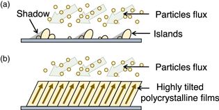
Fig. 9. (Color online) Schematic of tilted polycrystalline film structure resulting from self-shadowing effects during the glancing angle deposition (GLAD) process.
Download figure:
Standard image High-resolution imageThe c-axis-tilted ScAlN film with an Sc concentration of 30% was deposited on a (100) silicon substrate (SEIREN KST Corp.) using an RF magnetron sputtering system, as shown in Fig. 10. Table I lists the deposition conditions. The substrate tilt angle γ was set to 0°, 30°, 60°, and 90° to take advantage of the self-shadowing effects. As a sputtering target, an 80 mm diameter Al disc (Furuuchi Chemical Co.) was used, on which 3.2 g Sc ingots (JX Nippon Mining & Metals Co.) were placed. The target-substrate distance was 25 mm. A sputtering chamber was evacuated to a pressure below 3.0 × 10⁻⁴ Pa, and argon gas (99.999%) and nitrogen gas (99.999%) were introduced into the chamber. The deposition conditions were set to an Ar:N2-flow ratio of 2:1, sputtering pressure of 0.6 Pa, and RF power of 200 W with 13.56 MHz. The temperature of the cathode cooling water was set to 2 °C to cool the target. The thickness of the ScAlN films was controlled to 4.0–4.5 μm.
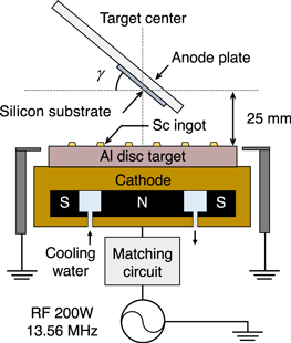
Fig. 10. (Color online) RF magnetron sputtering system for fabricating c-axis-tilted ScAlN film/silicon substrate structures.
Download figure:
Standard image High-resolution imageTable I. Deposition conditions.
| Al target | 80 mm dia., Purity 99.999% |
| Sc ingot | Purity 99.9% |
| RF power supply | 13.56 MHz, 200 W |
| Sputtering pressure | 0.60 Pa |
| Gas composition | Ar:N2 = 2:1 |
| Substrate temperature | Self-heating (300 oC) |
| Substrate tilt angle γ | 0°, 30°, 60°, 90° |
| Substrate-target distance | 25 mm |
| Target cooling water temperature | 2 °C |
The c-axis tilt angle and crystalline orientations of the samples were investigated using X-ray diffraction (XRD) with Cu Kα1 radiation. Figure 11 presents the χ-scan profile curves of the ScAlN (0002) pole of the samples. The χ angle at the ScAlN (0002) pole increased with the substrate tilt angle γ. The angle χ at the ScAlN (0002) pole corresponds to the c-axis tilt angle. Therefore, ScAlN films, which were deposited on silicon substrates using oblique particle flux, exhibit a c-axis-tilted orientation, and the tilt angle χ increases with the substrate tilt angle γ. The maximum c-axis tilt angle χ is 50.0°, which is obtained when the substrate tilt angle γ is 90°. The degrees of out-of-plane and in-plane crystalline orientations were evaluated by the full width at half maximum (FWHM) values for the χ-scan and ϕ-scan profile curves, respectively. Table II lists the FWHM values, along with the c-axis tilt angle χ, film thickness, and Sc concentration of the samples. In addition, Table II shows the theoretical K2 values of the Rayleigh-mode SAW for each sample when the wavelength λ is 8 μm and Sc concentration is 30%. The FWHM values of the χ-scan XRD were the smallest for the sample deposited at γ = 0°. No significant increase in the FWHM values was confirmed due to the c-axis tilt angle χ. In addition, the FWHM of the ϕ-scan XRD decreased with the c-axis tilt angle χ, and the minimum FWHM was 4.4o, which was obtained when the substrate tilt angle γ was 90o. This indicates that the highly c-axis-tilted ScAlN films on silicon substrates have a relatively high in-plane and out-of-plane crystalline orientation. However, the theoretical K2 value of SAW propagating in the Sc0.3Al0.7N film/silicon substrate structure is smaller than that of the Sc0.4Al0.6N film/silicon structure due to the relatively low piezoelectricity of the ScAlN films with an Sc concentration of 30%. The piezoelectric constant e33 of ScAlN films, which has a large effect on SAW excitation, increase monotonically until the Sc concentration reaches approximately 40%. 41) In addition, the ScAlN BAW velocity decreases as the Sc concentration increases. 8) The gap between the SAW velocities in ScAlN films and silicon substrates increases K2 value. Therefore, it is important to fabricate ScAlN films with an Sc concentration of 40% on silicon substrates to obtain a high K2 value.
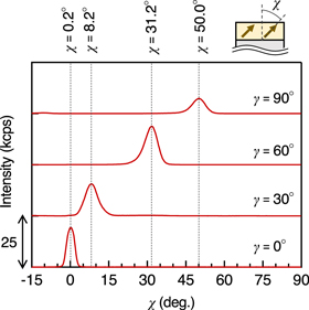
Fig. 11. (Color online) χ-scan profile curves of the ScAlN (0002) pole of the ScAlN films on the silicon substrate. The horizontal and vertical axes represent χ and the X-ray intensity, respectively. The angle χ at the ScAlN (0002) pole corresponds to the c-axis tilt angle.
Download figure:
Standard image High-resolution imageTable II. c-Axis tilt angle, crystalline orientation, film thickness, Sc concentration, and theoretical K2 value of ScAlN films on silicon substrates. The degrees of out-of-plane and in-plane crystalline orientations were evaluated by FWHM values for the χ-scan and ϕ-scan profile curves, respectively. The theoretical K2 values of Rayleigh-mode SAW for A and B structures are shown for each sample when the wavelength λ is 8 μm and Sc concentration is 30%.
| Substrate tilt angle γ | c-Axis tilt angle χ | χ-scan FWHM | ϕ-scan FWHM | Film thickness | Sc concentration | Theoretical K2 | |
|---|---|---|---|---|---|---|---|
| A | B | ||||||
| 0° | 0.2° | 3.2° | ― | 4.3 μm | 30.1% | 0.11% | 0.05% |
| 30° | 8.2° | 5.8° | 14.9° | 4.5 μm | 28.4% | 0.36% | 0.37% |
| 60° | 31.2° | 5.9° | 4.7° | 4.4 μm | 29.6% | 1.81% | 2.03% |
| 90° | 50.0° | 6.0° | 4.4° | 4.3 μm | 29.6% | 2.37% | 2.36% |
Figures 12(a) and 12(b) present cross-sectional SEM images of ScAlN films deposited at γ = 0° and 90°, respectively, on silicon substrates. Figure 12(a) shows that the ScAlN films have a columnar structure and grow perpendicular to the silicon substrates. Conversely, Fig. 12(b) shows that the columnar structure of the ScAlN films is significantly tilted. In addition, the thickness of the crystal grains is several hundred nanometers, which is larger than that shown in Fig. 12(a). These results are in good agreement with the χ-scan profile curves shown in Fig. 11 and the columnar structure of the polycrystalline films fabricated by the GLAD technique based on the self-shadowing effects. These results demonstrate that the c-axis-tilted ScAlN films grew on the silicon substrates due to the self-shadowing effects. The sputtering method using the self-shadowing effect is suitable for preparing c-axis-tilted ScAlN films on silicon substrates.

Fig. 12. Cross-sectional SEM images of ScAlN films deposited on silicon substrates at γ = (a) 0° and (b) 90°.
Download figure:
Standard image High-resolution image3.2. c-Axis-tilted ScAlN films with an Sc concentration of 40% grown on oxide-covered silicon substrates
The atomic arrangement of the substrates also affect the film growth. In general, films with an atomic arrangement close to that of the substrates are prone to grow on substrates. It has been reported that ScAlN films on diamond-like carbon do not crystallize when the Sc concentration exceeds 35%. 39) One reason is that the main phase is separated into AlN and ScN because of the atomic arrangement of the substrate. In this study, we attempted to prepare ScAlN films with an Sc concentration of 40% on (100) silicon substrates; however, the ScAlN films did not crystallize. This is because silicon has the same cubic structure as diamond-like carbon. This is a problem in SAW device applications, because the piezoelectricity of ScAlN films is maximized at an Sc concentration of 40%. In the semiconductor field, oxide-covered silicon substrates are used to electrically insulate semiconductor films and silicon substrates. Additionally, the SiO2 buffer layer is an effective method for eliminating the effect of the atomic arrangement of the substrates. 45,46) Therefore, we predicted that oxide-covered silicon substrates play the role of the SiO2 buffer layer.
The c-axis-tilted ScAlN film with an Sc concentration of 40% was deposited on an oxide-covered (100) silicon substrate (SEIREN KST Corp.) with an oxide film thickness of 300 nm. As a result of the theoretical analysis of K2 values, the 300 nm oxide film on the silicon substrate has almost no effect on the K2 value of SAW devices in the case of a wavelength λ of 8 μm. Table I lists the deposition conditions. The Sc ingots placed on the Al disc target weigh 3.4 g.
Figure 13 presents χ-scan profile curves of the ScAlN (0002) pole of the samples. ScAlN (0002) poles were observed in all ScAlN films prepared at various substrate tilt angles in the range of 0°–90°. This result shows that the thin buffer layer is effective in removing the influence of the atomic arrangement of the silicon substrate. In addition, although the peak intensity of the c-axis-tilted ScAlN films is smaller than that of the c-axis-oriented films, the c-axis tilt angle of the sample increased with the substrate tilt angle γ. The maximum c-axis tilt angle χ is 57.4°, which is obtained when γ is 90°. Table III lists the FWHM values, as well as the c-axis tilt angle χ, film thickness, and Sc concentration of the samples. In addition, Table III shows the theoretical K2 values of the Rayleigh-mode SAW for each sample when the wavelength λ is 8 μm and Sc concentration is 40%. Although the χ-scan FWHM values increase with angle γ, the ϕ-scan FWHM values decrease with the angle γ. The FWHM of the film deposited at angle γ = 90° was 5.2°. An appropriate in-plane crystal orientation of the highly c-axis-tilted ScAlN films was observed.
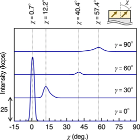
Fig. 13. (Color online) χ-scan profile curves of the ScAlN (0002) pole of the ScAlN films on the oxide-covered silicon substrate. The horizontal axis shows χ, and the vertical axis represents the X-ray intensity. The angle χ at the ScAlN (0002) pole corresponds to the c-axis tilt angle.
Download figure:
Standard image High-resolution imageTable III. c-Axis tilt angle, crystalline orientation, film thickness, Sc concentration, and theoretical K2 value of ScAlN films on oxide-covered silicon substrates. The degrees of out-of-plane and in-plane crystalline orientations were evaluated by FWHM values for the χ-scan and ϕ-scan profile curves, respectively. The theoretical K2 values of Rayleigh-mode SAW for A and B structures are shown for each sample when the wavelength λ is 8 μm and Sc concentration is 40%.
| Substrate tilt angle γ | c-Axis tilt angle χ | χ-scan FWHM | ϕ-scan FWHM | Film thickness | Sc concentration | Theoretical K2 | ||
|---|---|---|---|---|---|---|---|---|
| A | B | |||||||
| 0° | 0.7° | 3.6° | ― | 4.2 μm | 39.1% | 0.02% | 0.01% | |
| 30° | 12.2° | 5.6° | 12.7° | 4.3 μm | 39.8% | 1.12% | 1.73% | |
| 60° | 40.2° | 4.7° | 10.0° | 4.2 μm | 40.1% | 3.52% | 3.84% | |
| 90° | 57.4° | 8.8° | 5.2° | 4.3 μm | 39.7% | 3.88% | 3.76% | |
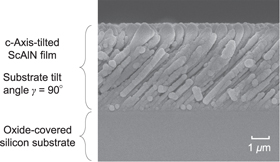
Figure 14 presents the cross-sectional SEM images of the ScAlN films deposited on silicon substrates at γ = 90°. The crystal grains are rounded due to the higher Sc concentration compared to those in Fig. 12. The crystal grains are thin near the silicon substrate, which then become thicker as the crystals grow. Moreover, the warpage of the crystal grains was confirmed. Consequently, the crystal orientation in the out-of-plane direction deteriorated in the sample with an Sc concentration of 40%. However, the technique for preparing highly c-axis-tilted ScAlN films with an Sc concentration of 40% is crucial. These results suggest a high potential for the fabrication of c-axis-tilted ScAlN films with an Sc concentration of 40% on silicon substrates and for SAW device applications using this structure.
Fig. 14. Cross-sectional SEM images of ScAlN films deposited on oxide-covered silicon substrates at γ = 90°.
Download figure:
Standard image High-resolution image
4. Conclusions
In this study, SAW propagation characteristics were theoretically analyzed to investigate the effect of the c-axis tilt angle on the electromechanical coupling coefficient K2 of SAWs propagating in the ScAlN film/silicon substrate structure. The Rayleigh-mode SAW propagation on the c-axis-tilted ScAlN film/silicon substrate layered structure was 3.88% and 3.90% in the A and B structures, respectively, and their K2 values were higher than those using the c-axis-oriented ScAlN films. Therefore, the c-axis-tilted ScAlN film/silicon substrate layered structure is suitable for Rayleigh-mode SAW devices. c-axis-tilted ScAlN films can be grown on silicon substrates via a sputtering method using the self-shadowing effect. The maximum c-axis tilt angle χ is 50.0°, and the highly c-axis-tilted ScAlN films on silicon substrates have a relatively high in-plane and out-of-plane crystalline orientation. These results indicate that the sputtering method using the self-shadowing effect can be implemented for preparing c-axis-tilted ScAlN films on silicon substrates. The crystallization of ScAlN films with an Sc concentration of 40%, which was not possible on bare silicon substrate because of the atomic arrangement of silicon, was enabled on oxide-covered silicon substrates. Highly c-axis-tilted ScAlN films with an Sc concentration of 40% can be prepared on them. The maximum c-axis tilt angle χ is 57.4°. There is room for quality improvement in the crystalline orientation of ScAlN films, as shown in Refs. 47 and 48. In the future, the application of this c-axis-tilted ScAlN films/silicon substrate-layered structure in SAW devices is greatly anticipated.