
Abstract
Flexible electronics with high-performance devices are crucial for transformative advances in several emerging and traditional applications. To address this need, herein we present p-type silicon (Si) nanoribbons (NR)-based high-performance field-effect transistors (FETs) developed using an innovative direct roll transfer stamping (DRTS) process. First, ultrathin Si NRs (∼70 nm) are obtained from silicon on insulator wafers using the conventional top-down method, and then the DRTS method is employed to directly place the NRs onto flexible substrates at RT. The NRFETs are then developed following the RT fabrication process which includes deposition of high-quality SiNx dielectric. The fabricated p-channel transistors demonstrate high linear mobility ∼100 ± 10 cm2 V−1 s−1, current on/off ratio >104, and low gate leakage (<1 nA). Further, the transistors showed robust device performance under mechanical bending and at a wide temperature range (15 °C–90 °C), showing excellent potential for futuristic high-performance flexible electronic devices/circuits.
Export citation and abstract BibTeX RIS

Content from this work may be used under the terms of the Creative Commons Attribution 4.0 license. Any further distribution of this work must maintain attribution to the author(s) and the title of the work, journal citation and DOI.
1. Introduction
High-speed, low-power flexible electronics are indispensable for several traditional and emerging applications such as wearables, soft robotics, mobile healthcare, human-machine interfaces etc. 1–6) One strategy to achieve this is to integrate the flexible ultra-thin chips on flexible foils. 7–10) This approach carries the advantage of conventional silicon-based complementary metal-oxide-semiconductor (CMOS) architecture to provide high-performance. This, though, complicates the packaging process and limits the flexibility of the processors. Further, the technology relies on conventional high-cost manufacturing processes and is based on an entirely subtractive process which leads to material wastage. Another approach is to develop processing circuits natively (directly) on flexible substrates adopting metal-oxide thin-film transistors (TFTs). 11,12) Recently, metal-oxide-based TFT technology has been used to develop a 32-bit flexible microprocessor. The limitation here is that only n-channel transistors can be fabricated because there is currently no viable p-type metal oxide material available for large-area commercial fabrication. 12–14) In this case, a more complicated layout based on n-channel transistors and resistors is needed to implement the logic functions. This will result in higher power consumption as compared with CMOS architecture which is detrimental to flexible electronics as higher power dissipation could degrade the plastic substrate. Moreover, the modest mobility of metal oxides leads to slower circuit operation (switching frequency—29 kHz). Whilst these are interesting developments, they do not meet the need for flexible CMOS circuits having a performance at par with conventional integrated circuits (ICs). This is much needed to drive advances in several application areas of flexible electronics.
Printed electronics based on high-mobility nanostructures could potentially be the solution to meet the above requirements. 9,15–17) Towards this, most works have focused on dry methods such as transfer or contact printing. 6,17–20) The transfer-based approach has attracted greater attention for realizing high-performance flexible electronic devices and circuits 21–23) as well as heterogeneous integration. The transfer-based approach allows the integration of silicon and compounds semiconducting nano to cm scale structures using elastomeric stamps. 4,15,24,25) For instance, transferred single-crystalline semiconductor Si nanoribbons (NRs) and nanomembranes (NMs) have been used to fabricate high-performance and flexible n-channel (NMOS) and p-channel (PMOS) transistors. 3,6,26–29) However, because of viscoelastic stamps used in the transfer process, it is challenging to obtain high transfer yield, registration, and reproducibility of these devices. 3) This is due to the unexpected tilt, orientation, and buckling of nanostructures under applied force during the transfer process. 30) Overcoming these challenges, recently, we have reported a simple, cost-effective, yet robust direct roll transfer stamping (DRTS) method to transfer high-mobility nanostructures over large areas (∼9 cm2) and on a wide variety of flexible substrates with registration <100 nm. 3,31) The method avoids the use of soft polymeric stamps, which reduces the chances of breakage, and wrinkling, etc of transferred nanostructures and hence helps to preserve their morphology and structure. The efficacy of this approach was shown by fabricating high-performance n-channel Si nanoribbons-based field-effect transistor (NRFETs) over flexible polyamide (PI) substrate. 3) Further, the potential of extending this approach towards high-performance printed CMOS circuits was demonstrated through a preliminary analysis of p-type NRFET presented at the SSDM 21 Conference. 31)
Advancing this work further, herein we present the in-depth analysis of direct roll transferred p-channel Si NR-based FETs. The distinct feature of the presented approach is that the high-quality silicon nitride (SiNx ) dielectric was deposited directly on the transferred Si NRs at RT using inductively coupled plasma-chemical vapor deposition (ICP-CVD) technique i.e. without any plasma related harmful effects. The fabricated devices have shown excellent device performance; charge carrier mobility of 100 ± 10 cm2 V−1 · s−1 and current on/off ratio >104. Further, we have done detailed electrical characterization under mechanical bending (40 mm) and a wide temperature range (15 °C–90 °C) conditions to confirm the robustness of fabricated transistors for high-performance flexible electronic circuits. The presented work on p-type FETs complements the previous realization of n-type FETs and opens new opportunities for realizing both device types on the same substrate and thus obtain in the future the much-needed high-performance printed CMOS circuits on diverse plastic substrates.
2. Experimental methods
2.1. Fabrication and selective doping of ultrathin Si NRs array using silicon on insulator (SOI) wafer
The Si NRs fabrication steps are similar to the description given in our previous work. 6) Briefly, the fabrication process involved patterning of Si NRs with a length of 55 μm and width of 5 μm using a lateral dry etching process. The Si NR arrays were patterned by lithography and reactive-ion etching (RIE) (CHF3/O2, 50 sccm, 55 mTorr, 5 min) to define the NRs geometries and expose the buried oxide (Box) layer. Thermal diffusion doping was performed on the source wafer to create ohmic contacts. The SiO2 diffusion barrier mask layer (thickness ∼ 250 nm) was deposited by using the plasma-enhanced chemical vapor deposition (PECVD). The openings of source and drain regions were performed using conventional photolithography steps. The resist served as a mask for selective dry etch process with a CH3/Ar plasma using RIE system (40 sccm CH3/Ar flow with a chamber base pressure of 30 mTorr, 200 W RF power). This step was carried out to etch the exposed areas of the oxide mask and open windows for diffusing boron in active regions (S/D) while the channel is covered by the SiO2 mask. The selective doping of the source and drain regions of NRs was performed using spin-on dopant (SOD) through thermal diffusion of boron (Filmtronics, P451). The furnace annealing was carried out to activate p-type dopants at 1050 °C in Ar ambient for 30 min. The doping concentration, measured using 4-point-probe, was found to be >1 × 10 18 cm–3. The etching of the SiO2 mask and Box layer was carried by hydrofluoric acid (HF) solution to obtain the suspended nanoribbons with delicate anchor points at both ends.
2.2. DRTS of Si NR
Custom-made DRTS set up 3) was used to carry out a reliable transfer of suspended Si NR arrays (selectively p-type doped) on SOI substrate. The DRTS is a single step (direct transfer) process. To carry out the direct roll-based transfer process, first, an adhesion promoter of ∼1.0 μm (PI-2545 precursor from HDmicrosystems) was applied on the commercial PI substrate. Next, Si NRs are brought into direct physical contact with the semi-cured PI receiver substrate. The applied force during roll transfer stamping is 12 N, and the roll speed is 0.1 mm s−1. After NR transfer, the PI substrate is subsequently cured at 250 °C for 2 h.
2.3. Si NRFET fabrication and characterization
After DRTS, p-channel transistors were fabricated using RT processes. This includes deposition of high-quality gate dielectric (SiNx , 100 nm) using ICP-CVD followed by metal deposition (Ti (10 nm)/Au (120 nm)) for gate, source, and drain using e-beam evaporation and lift-off. Electrical characterizations were performed using Cascade Micro-tech Auto-guard probe station interfaced with a semiconductor parameter analyser. Linkam PE120 Peltier system was used for heating and cooling the NRFETs to perform temperature dependence electrical measurements.
3. Results and discussion
3.1. DRTS of Si NRs and transistor fabrication
Figure 1 schematically shows the steps followed to fabricate p-channel NRFETs. As a first step, silicon NRs are fabricated on a rigid SOI wafer using a conventional nanofabrication process [Fig. 1(i)]. During this step, selective doping of the NRs was also carried out using SOD through the diffusion of boron to define source/drain (S/D) contact. This step produces an array of horizontally aligned and suspended NRs with well-defined channel lengths over SOI source wafers, which are eventually transferred to flexible receiver substrates using DRTS [Fig. 1(ii)]. The process is described in detail elsewhere. 3) Briefly, the source SOI wafer with released NR arrays is brought into direct physical contact with the semi-cured PI thin film over the receiver substrate. Partially cured PI enhances the adhesion between NRs and receiver substrate and helps to improve the transfer yield and registration factor. A transfer yield of 95% with a registration factor of <100 nm can be achieved using the DRTS process. Figure 2(a) demonstrates a top-view SEM image of a single Si NRs array in releasable form, ready for direct retrieval onto the target substrate. The inset of Fig. 2(a) shows a magnified image of the suspended NRs, anchored at both edges (5 μm width at both sides and supported by the underlying Box layer) to maintain the correct alignment and registration accuracy. To have a uniform and high transfer yield over a large area, conformal contact between the semi-cured PI layer and Si NRs is needed which we achieved by applying a high force of 12 N. But the use of semi-cured PI makes the direct transfer process slower. To overcome this drawback, UV-cured polymers, as an adhesive layer, could be used. 32) Following the DRTS of NRs, low-temperature steps (e.g. dielectric and metal deposition) were carried out to finalize p-channel NRFETs [Figs. 1(iii) and 1(iv)].

Fig. 1. (Color online) Schematic illustration of the fabrication steps involved in DRTS based Si NRFET fabrication: (i) suspended Si NRs with the selective p-type doped region, released by undercut etching of buried oxide on SOI, (ii) direct roll transfer stamping to transfer p-channel Si NRs on flexible substrate (PI), (iii) RT gate dielectric SiNx deposited by ICP-CVD on the transferred NRs, and (iv) metallization step to define source (S), drain (D) and gate (G) metal contacts to finalize the fabrication of flexible p-channel Si NRFETs.
Download figure:
Standard image High-resolution image
Fig. 2. (Color online) P-channel Si NR-based FET and its electrical characteristics: (a) SEM cross-sectional image of an anchored single Si NR array after etching away the Box layer. The inset shows the magnified image of the anchor point. (b) Transfer characteristics with VDS = −1 V in logarithmic and linear scales. The bottom inset shows an optical image of a typically fabricated transistor. (c) Output characteristics, and (d) transfer characteristics with varying VDS from −0.1 to −1 V.
Download figure:
Standard image High-resolution image3.2. Electrical characterization of p-channel Si NRFETs
The fabricated p-channel NRFETs with length ∼5 μm and width ∼45 μm (9 NRs of 5 μm width) on PI substrates were characterized in ambient dark conditions. The electrical characterization results of a typically fabricated p-channel FET device are shown in Figs. 2(b)–2(d). The transfer characteristics (IDS–VGS) with drain bias (VDS) of −1 V were obtained by varying gate-source voltage (VGS) from 3 to −2 V and shown in both linear and logarithmic scale in Fig. 2(b). Critical FET performance parameters to consider were extracted using the transfer scan: on-state (Ion), off-state current (Ioff), current on/off ratio (Ion/Ioff), effective mobility ( ), and subthreshold slope (SS).
33) The measured devices showed typical Ion (>10 μA)/Ioff (<1 nA) current ratio of >104 suggesting an excellent gate-channel control. The extracted SS from the logarithm transfer plot is 1 ± 0.3 V/decade. Large variation in SS suggests non-uniformity in the deposited SiNx
dielectric film and/or presence of interface traps between the channel and SiNx
interface non-uniformly. Further experiments are needed to confirm the exact reason for variation in SS. Next, threshold voltage (VT) was extracted using the linear extrapolation method. For this, the linear extrapolation of IDS–VGS graph, intercepting the Id = 0 at the x-axis (VGS) gives the VT value (0.6 V). This was followed by the calculation of transconductance (gm
), according to Eq. (1) shown below:
), and subthreshold slope (SS).
33) The measured devices showed typical Ion (>10 μA)/Ioff (<1 nA) current ratio of >104 suggesting an excellent gate-channel control. The extracted SS from the logarithm transfer plot is 1 ± 0.3 V/decade. Large variation in SS suggests non-uniformity in the deposited SiNx
dielectric film and/or presence of interface traps between the channel and SiNx
interface non-uniformly. Further experiments are needed to confirm the exact reason for variation in SS. Next, threshold voltage (VT) was extracted using the linear extrapolation method. For this, the linear extrapolation of IDS–VGS graph, intercepting the Id = 0 at the x-axis (VGS) gives the VT value (0.6 V). This was followed by the calculation of transconductance (gm
), according to Eq. (1) shown below:

The extracted gm
was used to calculate the field-effect (effective) mobility,  using Eq. (2) where W and L are the gate width and length respectively and COX stands for the dielectric capacitance (W/L = 45 μm/5 μm, thickness of SiNx
dielectric = 100 nm)
using Eq. (2) where W and L are the gate width and length respectively and COX stands for the dielectric capacitance (W/L = 45 μm/5 μm, thickness of SiNx
dielectric = 100 nm)

The extracted effective mobility was found to be ∼100 ± 10 cm2 V−1 s−1 which compares well with most of the state-of-the-art p-channel Si NR-based FETs. Further, the performance of DRTS p-channel NRFET is compared with the other p-channel devices fabricated using conventional transfer-based techniques (Table I).
Table I. Si micro/nanostructures-based flexible p-type FETs realised using transfer-based techniques.
| S. No | Transfer techniques | Si-structure morphology | Mobility (cm2 V−1 s−1) | ION/IOFF | Reference |
|---|---|---|---|---|---|
| 1. | Flip-transfer printing | Sub-μm membranes (340 nm thick) | 34 | ∼106 | 34 |
| 2. | Conventional transfer printing | Nanoribbons (100 nm thick) | 14 | 105 | 28 |
| 3. | Conventional transfer printing | Sub-μm ribbons (290 nm thick) | 85 ± 10 | ∼106 | 9 |
| 4. | Direct roll transfer stamping | Nanoribbons (70 nm thick) | 100 ± 10 | >104 | This work |
Next, the output characteristics (VDS–IDS) were obtained by varying VGS from 0 to −3 V with a step of 0.5 V. Notably, the low-VDS region shows a linear dependence of IDS with increasing VDS without any inflection point. This device characteristic (low-resistive metal–semiconductor (MS) contacts) is needed for achieving high device performance. Further, the output characteristics show strong drain current saturation (IDS
SAT) with increasing VDS, confirming the excellent gate-channel capacitive coupling. To confirm the MS contact ohmicity, we have calculated the ratio of the change in the saturation voltage (VDS
SAT) with VGS. In conventional transistors with ohmic contacts, a gradual channel approximation model is used to describe the drain current saturation:
33)
VDS
SAT ≈ [VGS − VT]. According to the theory, the ratio of the change in the saturation voltage with gate voltage, for FETs with ohmic contacts, would be close to unity. The fabricated p-channel devices showed  (confirming formation of ohmic contacts). Figure 2(d) shows the transfer characteristics of Si NRFET at various values of VDS. It is worth noting from Fig. 2(d) that the VT remains constant with varying VDS, indicating high stability charge transport behavior under different drain voltages. We have further studied the device stability under bending and varying temperature conditions in the following sections.
3.3. Stability analysis of flexible p-channel Si NRFETs
The mechanical robustness of the flexible p-channel NRFETs were evaluated under different bending conditions. We obtained the transfer characteristic under planar conditions after bending by mounting the device on 3D printed convex and concave structures both with a radius of curvature of 30 mm. The cyclic bending measurement was performed after every 10 cycles (up to 100 cycles). An optical image showing durability test by repeating device bending up to 100 times is included in the inset of Fig. 3(a). Using the transfer characteristics, variation in the on-current [Fig. 3(a)] and threshold voltage [Fig. 3(b)] of the device were extracted. The peak values of drain current were obtained at VGS = −3 V. As can be seen from this set of data, the Ion showed a 23% rise after 100 bending cycles. On the other hand, the VT of the device showed slight random variations initially (up to 60 °C) but it eventually stabilized to the initial VT value. This change in the electrical performance after bending could be attributed to the change of the band structure of the active material (Si), which affects the effective mass and hence the mobility of the charge carrier. 35–37) Such a bending-related variation in device performance could be solved by adding an encapsulation layer on top of the final device or by placing the device in the neutral plane. 27,38) This could enhance the bendability, device stability and also resolve the slight variation of the electrical properties under bending conditions. 27)

Fig. 3. (Color online) Variation of the IDS (a) and VT (b) measured in planar condition after compressive and tensile bending cycles at VDS = −1 V, VGS = −3 V. The inset of panel (a) shows optical images of devices during durability test when being under planar and bent conditions. The inset of (b) shows a photograph of flexible p-type NRFET arrays fabricated on PI substrate.
Download figure:
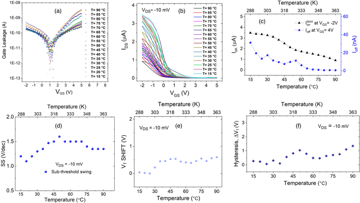
Standard image High-resolution imageThe temperature dependence device stability is also studied in this work [Fig. 4]. Before we measured the transfer characteristics, the gate leakage current was monitored at different temperatures of the present device under investigation. This was performed to evaluate the dielectric stability at different temperatures. The mechanical robustness of the RT deposited SiNx under different bending conditions was tested and reported in our previous work. 6) In this work, we have studied temperature-dependent stability. As shown in Fig. 4(a), there is one order decrease in gate leakage current from 3 nA 0.3 nA at 5 VGS when the temperature was increased from 15 °C to 90 °C. Although there is variation in leakage current, the values remain very low which confirms the high quality, and robustness of the RT deposited dielectric at a wide temperature range. Next, transfer scans [in the forward (+5 to −2 VGS) and reverse (−2 to +5 VGS) direction] were obtained at different temperatures (15 °C–90 °C with a step of 5 °C), as shown in Fig. 4(b). Important FET parameters were extracted using temperature varying transfer scans and are shown in different figure panels of Fig. 4. As can be seen in Fig. 4(b), the Ion of the device showed a sharp decrease after 35 °C with a stepwise increase in temperature. Similarly, Ioff showed a slight decrease with an increase in temperature. This could be explained through the increase of scattering events (acoustic-phonon assisted and Coulombic) in the channel and/or at the semiconductor/dielectric interface, which degrades the charge transport efficiency. 39) In fact, the gain in kinetic energy of the charge carrier, with increasing temperature, alters two distinct phenomena that could affect the charge transport in FETs (in the range of temperature we have performed measurements): (i) scattering events in the channel and/or channel/dielectric interface, and (ii) increase of thermionic current. Which one of these will dominate the charge transport depends on the nature of MS contact in FETs. For Schottky contacted FETs, the Ion and Ioff should show an increase in values. 33) This is because charge carriers acquire sufficiently high kinetic energy with increasing temperature to overcome the MS contact potential barrier and thus, the thermionic emission current component will increase. On the other hand, for an ideal ohmic contacted FETs, scattering events will dominate the charge transport as there will be a negligible increase in the thermionic emission part. As we showed above using the family of output scans, the FET device demonstrated the electrical behavior of a typical ohmic MS contact device which could explain the negative temperature dependence of FET current with temperature. To gain further insight on the decrease in Ion, we have analyzed other important FET parameters including SS, VT, and hysteresis. The change in SS with temperature change is shown in Fig. 4(d). This figure reveals that the absolute SS value increases sharply above RT (1.1 V/dec) up to 45 °C–50 °C (1.5 V/dec). After 50 °C, SS saturates, remains constant until 70 °C, and shows slight degradation after that. It is well known that the SS of a FET device is largely affected by the interface (channel/dielectric) trap charge density. Also, these interface charges lead to a shift in FET threshold voltage. To correlate the change in SS trend to interface traps, we have calculated the magnitude shift of VT with temperature [Fig. 4(e)]. The data in Fig. 4(e) shows a similar trend like SS change with temperature. Accordingly, both SS and VT change can be correlated to the transfer of mobile charges to immobile trapping states at the semiconductor/insulator interface. Finally, we have monitored the magnitude of these interface charges by calculating the hysteresis value (change in VT of forward and reverse transfer scan) at each temperature [Fig. 4(f)]. As expected, after 35 °C, there is a sharp increase of the hysteresis up to 50 °C–55 °C and then it saturates. The analyzed data shows a significant increase in the interface trap density above 30 °C–35 °C which leads to an increase in the scattering events at the channel/dielectric interface. Thus, the sharp decrease in the device on-current after 35 °C could be related to the thermal activation of interface traps that degrade the charge transport.
Fig. 4. (Color online) Temperature-dependent (15 °C–90 °C) electrical characterizations to investigate the stability of p-channel NRFETs. (a) Gate dielectric leakage current, and (b) transfer scans. Important FET parameters data extracted using temperature-dependent transfer scans: (c) on-current and off-current, (d) S–S, (e) VT, and (f) hysteresis.
Download figure:
Standard image High-resolution image
4. Conclusions
We have demonstrated a new route for obtaining high-performance p-type Si NRs arrays-based FETs on flexible substrates. The DRTS approach used here showed excellent yield and registration of nanoscale transferred structures, which are difficult to be achieved using the conventional transfer method. The contamination-free transfer of Si NRs was confirmed by the fabrication of high mobility p-channel NRFETs using the RT fabrication process. The fabricated transistors showed high device mobility (∼100 cm2 V−1 s−1), and current on/off ratio (>104). We also showed the high device robustness to mechanical bending (40 mm) and at a wide temperature range (15 °C–90 °C). The results presented here confirm the high quality of RT deposited dielectric over a wide temperature range (maximum gate leakage current of 3 nA at 5 VGS, 15 °C). Finally, analyzing the temperature-dependent transfer scans, we showed the role played by interface traps towards degrading the on-current of the device. We believe that the demonstrated DRTS approach and fabricated p-channel NRFETs have the potential for realizing the high-performance large-area flexible CMOS circuits.
Acknowledgments
This work was supported in part by Engineering and Physical Sciences Research Council (EPSRC) through Engineering Fellowship for Growth (EP/R029644/1) and Heteroprint Programme Grant (EP/R03480X/1).