
Abstract
Crystalline germanium (c-Ge) is an attractive material for a thin-film transistor (TFT) channel because of its high carrier mobility and applicability to a low-temperature process. We present the electrical characteristics of c-Ge crystallized by an atmospheric-pressure micro thermal plasma jet (μ-TPJ). The μ-TPJ-crystallized c-Ge showed a maximum Hall mobility of 1070 cm2 V−1 s−1 with a hole concentration of ∼1016 cm−3, enabling us to fabricate a TFT with a field-effect mobility (μFE) of 196 cm2 V−1 s−1 and an ON/OFF ratio (RON/OFF) of 1.4 × 10⁴. RON/OFF and μFE were dependent on the scanning speed of the TPJ, implying different types of defects were induced in the channel regions. These findings show the possibility of TPJ irradiation as a promising method for making c-Ge TFTs on insulating substrates.
Export citation and abstract BibTeX RIS
1. Introduction
Thin-film transistor (TFT) technology has contributed to a marked improvement in industry. 1–5) Hydrogenated amorphous silicon (a-Si:H) TFTs, for instance, have been widely utilized in various ways. 6–9) However, devices that require higher mobility beyond that of a-Si:H TFTs lead us to a quest for alternative channel materials. Crystalline germanium (c-Ge) possesses a lot of attractive advantages in that context. Not only its high carrier mobility (electron: 3900 cm2 V−1 s−1; hole: 1900 cm2 V−1 s−1) but also its suitability for a low-temperature process, owing to a relatively low melting point, is a great advantage. 10,11) We can trace a long history of low-temperature syntheses of Ge TFTs and it is still a major topic of study.
To form a high-quality c-Ge film on an insulator, various crystallization techniques such as solid-phase crystallization (SPC), 12–14) rapid thermal annealing based on the seed layer technique, 15) metal-induced crystallization, 16–18) laser annealing, 19) and flash lamp annealing 20) have been proposed. Besides these techniques, we have proposed the application of an atmospheric-pressure DC arc discharge micro thermal plasma jet (μ-TPJ) to the rapid crystallization of amorphous group IV semiconductor films on insulators. Depending on the irradiation conditions, SPC, leading-wave crystallization (LWC), high-speed lateral crystallization (HSLC), and granular crystal growth of a-Si have been observed in the microsecond time domain on the basis of high-speed camera (HSC) observations. 21–24) However, in the case of ultra-rapid crystallization of a-Ge, there is almost no report on its mechanism. In addition, the relationship between the crystallization mechanism and the resulting electrical characteristics such as carrier concentration and mobility is still a matter of research.
In this work, we attempt to get insights into the rapid phase transformations of a-Ge during μ-TPJ irradiation and investigate the approach to obtaining superior electrical characteristics of c-Ge on insulators. Based on an understanding of c-Ge crystallization using TPJ irradiation, we fabricated p-type top-gate TFTs and discuss their device characteristics.
2. Experimental methods
2.1. Crystallization of a-Ge films
Non-doped a-Ge films of 100 nm thickness were formed on quartz substrates by plasma-enhanced chemical vapor deposition (PECVD) at 200 °C using GeH4 diluted in H2. The μ-TPJ was generated by DC arc discharge under atmospheric pressure with a supply power (P) ranging from 0.5 to 1.4 kW between a W cathode and a Cu anode separated by 2.0 mm (ES) (Fig. 1). The Ar gas flow rate (f) was varied from 1.0 to 2.0 l min−1. The μ-TPJ was formed by blowing out the thermal plasma through an orifice with a diameter of 600 μm. The substrate was linearly moved by a motion stage in front of the μ-TPJ with a scanning speed (v) ranging from 600 to 3000 mm s−1. The distance between the plasma source and the substrate (d) was varied from 1.0 to 2.0 mm. For in situ observation of the grain growth of a-Ge films during μ-TPJ irradiation, an optical microscope and an HSC were set on the motion stage on the backside of the substrate. The frame rate (Rf) was set at 165 000 frames per second. To search for the conditions of HSLC, a-Ge islands with lengths (L) of 2–27 μm and widths (W) of 2–47 μm were patterned by photolithography and subsequent wet etching. As described in detail below, capping SiO2 layers were formed by remote PECVD at 200 °C using SiH4, O2, and Ar gases. Micro-Raman scattering spectral analysis was used to evaluate the crystallinity of the μ-TPJ-irradiated samples. The carrier concentration and mobility were measured by Hall effect measurement. The grain size and grain boundaries (GBs) were investigated by the electron backscattering diffraction (EBSD) method.

Fig. 1. (Color online) Schematic image of the experimental setup for the μ-TPJ irradiation.
Download figure:
Standard image High-resolution image2.2. TFT fabrication
P-type top-gate TFTs were fabricated using Ge films crystallized by μ-TPJs by the following process steps. A non-doped a-Ge film with a thickness of 100 nm was deposited by PECVD with the same conditions as mentioned above. A TFT channel with W of 2 μm and L of 5 μm was patterned. After deposition of a 550 nm thick SiO2 capping layer, the μ-TPJ was irradiated to the samples with the conditions of P = 1.1–1.4 kW, f = 1.0 l min−1, d = 2.0 mm, and v = 800–1800 mm s−1. After removal of the SiO2 capping layer, 90 nm thick gate SiO2 was formed by remote PECVD at 350 °C. Then, source and drain regions were formed by B+ ion implantation with an acceleration voltage of 35 keV and a dose of 1.0 × 1015 cm−2 using a resist mask. The impurities in the source and drain regions were activated by an electric furnace at 550 °C for 10 min in ambient N2. Source, drain, and gate electrodes were formed by evaporation of Al after opening contact holes by wet etching.
3. Results and discussion
Figure 2(a) shows a typical phase diagram with μ-TPJ conditions of d = 1.0 mm, f = 1.5 l min−1, and v = 1600–3000 mm s−1. After μ-TPJ irradiation on a-Ge films, we found three different phases, that is, an amorphous phase (no phase transformation), LWC, and film stripping. Observation of the growth process using the HSC showed that explosive crystallization occurred intermittently as shown in Fig. 3(a), which is evidence for LWC. 23) Figure 3(b) shows a typical EBSD image of an enlarged part of the LWC region. The LWC region is composed of three parts from the viewpoint of the size of the grain: (1) fine grains without a specific crystal orientation; (2) an intermediate region; and (3) relatively large grains of W = 1 μm and L = 5–10 μm. The Raman scattering spectrum at each part indicates the high crystallinity of LWC-Ge over the whole LWC region [Fig. 3(c)]. Therefore, both part (1) and part (2) are also crystallized and made up of rather fine grains, which seem not to be crystallized from the EBSD image. One can predict that the solid-state crystal growth of Ge takes at the shortest 1 ms. 25,26) In contrast, the HSC image indicates that the crystallization induced by the TPJ irradiation was completed in 6 μs, which was derived from the frame rate of the HSC. Thus, we suppose that TPJ-crystallized Ge goes through an amorphous-liquid transition, not an amorphous-solid transition. 27) This finding leads us to an answer to why the SPC phase does not appear in the case of Ge.

Fig. 2. (Color online) Phase diagram of μ-TPJ-irradiated Ge film with respect to P and v. The distance between the plasma source and the a-Ge films was 1.0 mm and the Ar gas flow rate (f) was set at 1.5 l min−1.
Download figure:
Standard image High-resolution image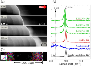
Fig. 3. (Color online) (a) HSC snapshots of Ge film during μ-TPJ irradiation (P = 0.85 kW, d = 1.0 mm, f = 2.0 l min−1, v = 1400 mm s−1) of 100 nm thick a-Ge films. (b) EBSD image of the crystallized Ge film by μ-TPJ irradiation under LWC conditions. The typical length of LWC is depicted by broken lines. (c) Raman spectra of μ-TPJ-irradiated Ge films and as-deposited a-Ge film. As a reference, the spectrum of a single-crystalline Ge wafer is also shown.
Download figure:
Standard image High-resolution imageBased on an understanding of the mechanism of LWC-Ge induced by TPJ irradiation, we examined the possibility of applying LWC-Ge to a channel of TFT devices. Since a GB deteriorates device performance, a TFT channel should contain as little GB as possible. In this respect, LWC-Ge has a disadvantage in that the fine grain is formed in the initial growth region as mentioned above. We supposed that a relatively higher crystallization velocity of ∼14 m s−1 (that of Si is ∼4–5 m s−1) 23) causes a number of collapses among grains during growth, resulting in a small size of the grain. Thus, LWC-Ge might be difficult to employ in device applications, so we paid attention to another crystal phase, that is, HSLC.
According to our previous researches on a-Si crystallizations by using TPJ irradiation, HSLC-Si shows larger grains (∼5 μm wide and ∼60 μm long). 22) We explained the crystallization mechanism of HSLC as follows: a Si film beneath a μ-TPJ is melted and then long-grain growth is caused by a strong lateral temperature gradient induced by high-speed scanning of the melting region. Figures 4(a) and 4(b) show a SEM image after the TPJ irradiation condition in which Ge is expected to melt completely. In contrast to the case of Si, agglomeration of Ge leads to film stripping and HSLC cannot be achieved on planar Ge films. Ge agglomeration was also reported in studies on lateral liquid-phase epitaxy. 28–31) This type of crystal growth is known as Volmer–Weber growth or Stranski–Krastanov growth, 32) where interfacial free energy and lattice mismatch determine which growth modes are predominant. Hashimoto et al. 28) systematically investigated the effect of interfacial free energy by introducing three different oxide layers between an a-Ge film and a Si substrate. They pointed out that Ge agglomeration is suppressed by introducing La2O3 with low interface energy with liquid Ge, leading to the crystallization of a 44-μm-long single Ge wire. In this study, instead of introducing such oxide layers at the interface with the substrate, we simply put a capping layer that has been applied to zone-melting c-Ge growth by Takai et al. 33) Therefore, we examined the availability of the SiO2 capping layer for TPJ crystallization. Figures 5(a) and 5(b) show SEM images of formed Ge islands with 550 nm thick capping SiO2 layers on them. After TPJ irradiation, we could melt and crystallize the a-Ge islands without severe agglomeration in strips with a width of ∼2 μm [Fig. 5(b)]. This HSLC-Ge strip possesses good crystallinity comparable to that of single-crystalline Ge [Figs. 3(c) and 5(c)]. Thus, we concluded that the SiO2 capping layer was available to suppress Ge agglomeration even for TPJ crystallization in melting and regrowth conditions.
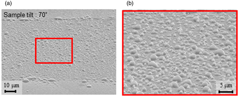
Fig. 4. (Color online) (a) SEM image of the crystallized Ge film after μ-TPJ irradiation with LWC conditions. (b) An enlarged SEM image corresponding to the red box in (a), which clearly shows agglomeration of Ge.
Download figure:
Standard image High-resolution image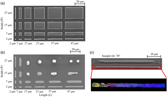
Fig. 5. (Color online) SEM images of (a) the patterned 100 nm thick a-Ge and (b) that crystallized by TPJ irradiation (P = 1.55 kW, d = 1.0 mm, f = 1.5 l min−1, v = 1600 mm s−1). (c) SEM image and EBSD mapping of Ge islands (2 μm × 47 μm) after μ-TPJ-induced melting and HSLC.
Download figure:
Standard image High-resolution imageAiming to expand this crystallization technique to device fabrication, we patterned strip channels and evaluated crystallinity after TPJ irradiation. EBSD mappings and GB mappings of LWC-Ge and HSLC-Ge are shown in Fig. 6. In LWC conditions, only fine grains (∼100 nm) are formed and their GBs are mostly random [Figs. 6(a) and 6(b)]. In contrast, HSLC-Ge shows lateral long grains (∼10 μm) with predominant Σ3 coincidence boundaries. In this case, random GBs are completely eliminated from the active channel region as depicted by the dotted box in Figs. 6(c) and 6(d). Figure 7 shows the hole concentration and mobility of Ge films crystallized under LWC and HSLC conditions. It is clearly seen that LWC-Ge with fine grains and random GBs shows high hole concentration in the order of ∼1018 cm−3, and Hall mobility lower than 100 cm2 V−1 s−1. In contrast, HSLC-Ge shows a low hole concentration of ∼1016 cm−3 and the maximum Hall mobility reaches 1070 cm2 V−1 s−1. In general, GBs generate holes in polycrystalline Ge and result in low Hall mobility. 34) The results of Hall effect measurements seem to reflect the elimination of random GBs.
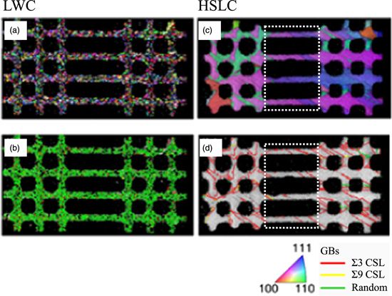
Fig. 6. (Color online) EBSD mapping (a) and GB mapping (b) of Ge strip channel pattern crystallized under LWC conditions and those under HSLC conditions for (c) and (d). Random GBs of fine grains in LWC-Ge are drastically eliminated in HSLC-Ge.
Download figure:
Standard image High-resolution image
Fig. 7. (Color online) Hole concentration and mobility of Ge films crystallized under LWC and HSLC conditions. The inset optical micrographic images show a typical sample for Hall measurement.
Download figure:
Standard image High-resolution imageBased on the above investigation, we attempted to demonstrate TFT operation using HSLC-Ge films crystallized by TPJ irradiation. Although operation could not be confirmed for LWC-Ge, which would be due to the large number of GBs, TFT operation was confirmed for HSLC-Ge. The transfer characteristics of 10 TFTs fabricated using HSLC films are shown in Fig. 8. The TFT dimensions are L = 5 μm and W = 2 μm. The HSLC-TFT reaches a field-effect mobility (μFE) of 196 cm2 V−1 s−1 as its maximum and shows a high ON/OFF ratio (Ron/off) of ∼104, which is high enough to be applicable to peripheral high-speed driver circuits. On the other hand, we found that crystallized conditions, v, strongly affected the resultant device performance. Figure 9(a) shows the transfer characteristics of the TFT fabricated by HSLC with various v. Although each μFE is as high as 130 cm2 V−1 s−1, off current drastically varies in the range of ∼10−7 to ∼10−9 A in the HSLC-TFT with a lower v less than 900 mm s−1 and in that with a higher v more than 1000 mm s−1 [Figs. 9(b) and 9(c)]. For further investigations on defects, we examined the temperature dependency of the fabricated TFTs. 35) Figure 10 shows the transfer characteristics measured at different temperatures in the range of 25 °C–100 °C. A drastic shift of threshold voltage is observed in the sample crystallized with v = 800 (≤ 900) as T increases, while just a slight shift is observed in that crystallized with v = 1700 (≥ 1000). This result implies that the TFT crystallized with v ≤ 900 contains a defect that is annealed out through a rise of temperature up to 100 °C, which would not be formed under the condition v ≥ 1000. The conductivities (σ) at Vg near the rising edge of the transfer characteristics, where a flat band situation is considered to be realized, are plotted as a function of the reciprocal of temperature (T = 25 °C–100 °C) in Fig. 11(a). The samples crystallized with v ≤ 900 show gentler slopes than those with v ≥ 1000. EBSD images showed no correlation with GBs, which are often considered as a possible source of hole generation [Fig. 11(b)]. Therefore, the observed variations are most likely to be ascribed to intra-grain defects. Assuming that the variations of the slopes are associated with different defect levels in the bandgap, we estimated the activation energy (Ea) by using the equation
Here, A and kB are a coefficient and Boltzmann's constant, respectively. A lower Ea of 0.06 eV was estimated in the samples crystallized with v ≤ 900, but a relatively higher Ea of 0.20–0.28 eV was estimated in those with v ≥ 1000. We suppose that vacancies are related to a mechanism of formation of the different types of defects observed in this study. The self-diffusion coefficient increases as a function of temperature and, furthermore, is enhanced in liquid Ge. 35–38) Stojić et al. pointed out the importance of vacancies in a self-diffusion mechanism in liquid Ge, where, without vacancies, the estimated jumping distance could not match the experimental results. Since a-Ge:H contains a large number of Ge dangling bonds, the formation of defects in HSLC-Ge, which goes through the liquid phase, would be also dominated by self-diffusion via vacancies. In the scheme of TPJ crystallization, the maximum temperature decreases while the maximum heating/cooling rate increases with an increase of v. 39,40) The maximum temperature would vary with the attempt frequency of jumps of vacancies, and the heating/cooling rate would determine how far vacancies could move. Thus, TPJ crystallization with different v yields a variation in the formation of defects. The details of the maximum temperature and the heating/cooling rate should be required to identify the observed defects. An optical-interference contactless thermometer will enable us to gain deep understanding of defects in HSLC-Ge, as in the case of Si, in the near future. 41–43)

Fig. 8. (Color online) Id–Vg characteristics (transfer characteristics) and field-effect mobility of TFT fabricated by μ-TPJ-crystallized Ge on a quartz. A schematic cross-sectional image of the prepared TFT and its optical micrographic image are shown on the bottom left and right, respectively.
Download figure:
Standard image High-resolution image
Fig. 9. (Color online) (a) Transfer characteristics of HSLC-Ge TFTs with various scanning speeds, v. Both (b) field-effect mobility (μFE) and (c) off current are affected by v.
Download figure:
Standard image High-resolution image
Fig. 10. (Color online) Variations of the transfer characteristics with temperature (T).
Download figure:
Standard image High-resolution image
Fig. 11. (Color online) (a) Arrhenius plot of conductivities at the gate voltages near the rising edge of the transfer characteristics. Fitting curves are also drawn as dotted lines. (b) Histograms of types of GBs for μ-TPJ-crystallized Ge with v ≤ 900 (left) and v ≥ 1000 (right).
Download figure:
Standard image High-resolution image4. Conclusions
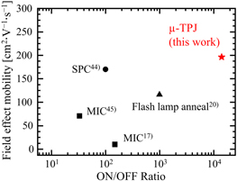
We formed crystalline germanium (c-Ge) thin films on quartz substrates by using atmospheric-pressure micro thermal plasma jet (μ-TPJ) irradiation onto a-Ge films deposited at 200 °C. By adjusting the surface area of the films and the thickness of SiO2 capping layers, we successfully induced high-speed lateral crystallization (HSLC) and obtained a quasi-monocrystalline c-Ge strip with 2 μm × 47 μm. Such HSLC-Ge showed a maximum Hall mobility of 1070 cm2 V−1 s−1, resulting from the suppression of grain boundary formation. We expanded this crystallization technique to top-gate TFT fabrication, whose channels were crystallized with conditions similar to those of HSLC. The maximum field-effect mobility of 196 cm2 V−1 s−1 with a high ON/OFF ratio of ∼104 clearly shows the potential of μ-TPJ irradiation for next-generation TFTs on insulating substrates (Fig. 12). On the other hand, we found that the scanning speed (v) of μ-TPJ irradiations strongly affects the resultant device performance, resulting from the formation of different types of defects (activation energy of 0.06 and 0.20–0.28 for v ≤ 900 and v ≥ 1000, respectively). In situ temperature measurement during μ-TPJ irradiation will pave the way toward further improvements on TFTs using HSLC-Ge.
Fig. 12. (Color online) Benchmark of electrical performance of p-type Ge transistors fabricated on insulating substrates in terms of mobility and ON/OFF ratio.
Download figure:
Standard image High-resolution image
Acknowledgments
Part of this work is supported by JSPS KAKENHI (Grant-in-Aid for Young Scientists, Grant No. 21K14547). This work is also partly supported by the Adaptable and Seamless Technology Transfer Program through Target-Driven R&D from the Japan Science and Technology Agency, Grant No. JPMJTR20RS. Part of this research was supported by the Research Institute for Nanodevice and Bio Systems, and the Natural Science Center for Basic Research and Development, Hiroshima University.