
Abstract
Based on our recent studies, we review our proposed experimental method for evaluating internal quantum efficiency, which is a critical parameter for semiconductor light-emitting device performance. We validated our evaluation method by comparing the results of the efficiency curve analysis using an exciton rate equation model with the results of radiative and nonradiative recombination dynamics obtained by time-resolved photoluminescence spectroscopy. We also review the characteristics of the stimulated emission observed from optically pumped AlxGa1−xN-based multiple quantum wells. The most important finding was the contribution of excitons to optical gain formation. The excitonic gain is expected to decrease the threshold carrier density for stimulated emission and lead to higher performance of semiconductor laser diodes.
Export citation and abstract BibTeX RIS
1. Introduction
The III-nitride semiconductors GaN and AlN have direct wide bandgaps of 3.4 and 6.1 eV, respectively, and thus Alx Ga1−x N ternary alloy semiconductors have a bandgap tunability in the ultraviolet (UV) to deep-UV spectral range. Alx Ga1−x N ternary alloy semiconductors are promising candidates for solid-state light sources, such as light-emitting diodes (LEDs) and laser diodes (LDs), operating in the UV-A (320–400 nm), UV-B (280–320 nm), and UV-C (200–280 nm) ranges of the electromagnetic spectrum. Demand is increasing for Alx Ga1−x N-based LEDs with high luminescence efficiency because they can be used in various UV applications. 1–5) For example, UV-A devices are used in UV curing and UV-B devices are used in phototherapy. UV-C devices are promising for water purification and sterilization. UV-B and UV-C devices may also be suitable for biomedical photonics, analytic sensing, coronavirus inactivation, and other applications. Alx Ga1−x N-based LDs exhibit great potential as promising alternatives to current UV light sources, such as gas lasers, excimer lasers, and solid-state harmonic lasers, and much research has focused on realizing these applications in the last few decades. The development of UV light-emitting devices using Alx Ga1−x N-based multiple quantum wells (MQWs) has advanced rapidly in recent years. UV-C LEDs with an emission wavelength of 275 nm achieved a high external quantum efficiency (EQE) of 20.3%. 6) The room-temperature operation of UV-C LDs 7–10) with an emission wavelength of 271.8 nm and UV-B LDs 11–14) with an emission wavelength of 298 nm has been demonstrated under pulsed current injection. However, the performance of Alx Ga1−x N-based LEDs and LDs still requires improvement. The luminescence efficiency of Alx Ga1−x N-based LEDs is insufficient for commercial applications, and the operating current density of Alx Ga1−x N-based LDs is high and must be decreased to improve the device stability and lifetime.
GaN and AlN have large exciton binding energies of 25 and 57 meV, 15) respectively; thus, the binding energy of excitons in Alx Ga1−x N ternary alloy semiconductors is expected to be larger than the thermal energy at room temperature (kB T = 26 meV). Owing to the advantages of excitonic behavior, the excitons in Alx Ga1−x N are stable at high excitation densities, where the interaction between two or more excitons results in the unique properties characterized by the formation of biexcitons and inelastic scattering of excitons. Alx Ga1−x N is a particularly good candidate for exploring the intrinsic recombination processes of high-density excitons. In our work to date, we have investigated the dense excitonic properties of Alx Ga1−x N ternary alloy epitaxial layers and measured the binding energies of biexcitons in Ga-rich (x = 0.019–0.092), intermediate (x = 0.61), and Al-rich (x = 0.81 and 0.89) Alx Ga1−x N epitaxial layers. 16–18) We observed a large bowing in the compositional dependence of the biexciton binding energy that resulted from the localization due to alloy disorder greatly increasing the biexciton binding energy. 19) We have also examined how quantum confinement affects biexcitons in Alx Ga1−x N-based MQWs. We observed the confinement-enhanced biexciton binding energy over 150 meV and determined the effects of quantum confinement and localization on the biexciton binding energy separately. 20,21) Biexciton luminescence was clearly observed up to 750 K and the luminescence lines from the inelastic scattering processes of excitons and biexcitons appeared and became more prominent as the temperature was increased up to 750 K. 22) For excitonics (exciton engineering), clarifying the recombination dynamics of dense excitonic phenomena is important because the contribution of excitonic processes to optical transitions is predicted to improve the performance of light-emitting devices; efficient radiative exciton transitions can increase device efficiency.
Excitonic processes can also contribute to optical gain formation and are expected to decrease the operating current density of LDs. The contribution of excitonic transitions to optical gain formation has been investigated thoroughly in wide-bandgap II–VI semiconductors. Ding et al. 23) reported the first experimental evidence for excitonic gain in II–VI MQW structures. They explained the optical gain formation in a Cdx Zn1−x Se/ZnSe MQW structure by considering a partial phase-space-filling effect of excitons in the lower-energy states of inhomogeneously broadened exciton resonance. Subsequently, several studies explored the exciton-related mechanisms of optical gain formation in wide-bandgap II–VI MQW structures. 24–28) The contribution of biexcitons to optical gain formation was also observed in Cdx Zn1−x Se/ZnSe MQW, 29) ZnSe/Znx Mg1−x Sy Se1−y single quantum well, 30) and Cdx Zn1−x S/ZnS MQW 31,32) structures. The studies showed that the threshold carrier density for optical gain formation and resultant stimulated emission (STE) arising from the excitonic transition processes is on the order of one-tenth or one-hundredth of that based on degenerate electron–hole plasma (EHP). Therefore, the excitonic transition processes are important for improving the performance of Alx Ga1−x N-based LEDs and LDs further.
To improve the performance of light-emitting devices, the luminescence efficiency should be evaluated. EQE is one of the best parameters for evaluating light-emitting device performance and is given approximately by the product of internal quantum efficiency (IQE), carrier injection efficiency (CIE), and light extraction efficiency (LEE). Consequently, to improve EQE, the IQE, CIE, and LEE components should be evaluated and improved separately. However, there is no direct experimental method for measuring these components and the best estimate must be used. For estimating IQE, several procedures based on optical measurements have been reported, 33–36) and we proposed a procedure based on temperature- and excitation power density (EPD)-dependent photoluminescence (PL) spectroscopy. 33,34) We used our procedure to estimate the EPD dependence of the IQE in III-nitride semiconductors. The IQE depended strongly on the EPD at low EPDs, even at low temperatures of less than 10 K, at which the IQE increased with increasing EPD. This result showed that the nonradiative recombination centers (NRCs) are active, even at low temperatures. Therefore, PL efficiency should be measured as a function of EPD, and the dependence of IQE on injected carrier density should be considered.
A method for analyzing the EPD dependence of IQE based on the rate equations of the radiative and nonradiative recombination processes of carriers (the ABC model) is frequently used to analyze IQE in III-nitride semiconductors. 37,38) However, because of the large exciton binding energy in III-nitride-based MQWs, exciton recombination processes are expected to play a main role in band-edge optical transitions, even at room temperature. Therefore, exciton recombination processes should be considered in analyzing the IQE in III-nitride-based MQWs. We have proposed a rate equation model based on the radiative and nonradiative recombination processes of excitons for analyzing the EPD dependence of the IQE in Inx Ga1−x N-based and Alx Ga1−x N-based MQWs. 39–41) We demonstrated that the exciton rate equation model was applicable and valid for III-nitride-based MQWs.
In this article, we review our recent experimental studies on Alx Ga1−x N-based UV-A 41) and UV-C 42) MQWs. We aim to provide a comprehensive understanding of Alx Ga1−x N-based MQWs from their fundamental optical properties to their optical functionality. First, we review our proposed experimental method for evaluating IQE in Alx Ga1−x N-based UV-A MQWs by using temperature- and EPD-dependent PL spectroscopy. We verify the validity of our evaluation method by comparing the results of the IQE curve analysis using the exciton rate equation model with the radiative and nonradiative recombination dynamics obtained by time-resolved photoluminescence (TRPL) spectroscopy. Next, we review the characteristics of the STE observed from optically pumped Alx Ga1−x N-based UV-C MQWs. The most important finding is the contribution of excitons to optical gain formation and the resultant STE. Finally, we present our latest experimental results on the STE properties. We demonstrate the lowest threshold for STE from Alx Ga1−x N-based UV-C MQWs grown on sapphire substrates and the excitonic optical gain formation up to 450 K.
2. Experimental procedure
In this section, we describe the sample fabrication and PL measurements performed in our previous studies. 41,42) Alx Ga1−x N-based UV-A and UV-C MQW structures were grown by metalorganic vapor phase epitaxy. A UV-A MQW sample was grown on a c-plane sapphire substrate following deposition of a 4 μm thick undoped AlN layer, a 2 μm thick n-Al0.53Ga0.47N layer, a 200 nm thick n-Al0.42Ga0.58N layer, a 1 μm thick Al0.24Ga0.76N layer, and a 200 nm thick n-Al0.18Ga0.82N layer. The MQW structure consisted of three periods of 3 nm thick Al0.18Ga0.82N well layers separated by 12 nm thick Al0.32Ga0.68N barrier layers. The PL spectrum from the well layers contained a single peak and the PL peak wavelength at room temperature was about 325 nm under weak excitation. The structure and quality of the sample were similar to those reported previously. 43) A UV-C1 MQW was also grown on a c-plane sapphire substrate following deposition of a 4 μm thick AlN layer, a 2 μm thick Al0.65Ga0.35N cladding layer, and an 80 nm thick Al0.55Ga0.45N optical confinement layer (OCL). The MQW structure consisted of three periods of 2 nm thick Al0.45Ga0.55N well layers separated by 8 nm thick Al0.55Ga0.45N barrier layers. The bottom barrier layer was grown on the 80 nm thick OCL, and the sample was terminated with an 8 nm thick barrier layer. All the layers were intentionally undoped.
PL measurements were carried out using the second-harmonic light emitted from a wavelength-tunable dye laser pumped by a Xe–Cl excimer laser (308 nm). The pulse width was 20 ns, the repetition rate was 100 Hz, and the excitation wavelength was set to 240 nm which corresponded to the band-to-band excitation of both well and barrier layers. A liquid-nitrogen-cooled charge-coupled-device camera combined with a single-grating monochromator (focal length: 50 cm; grating: 2400 grooves mm−1) was used to detect the PL signal. We estimated the spectral resolution to be better than 0.05 nm (i.e. less than 1.0 meV at approximately 5 eV). The back-scattering configuration was used for all IQE measurements. STE were measured in the edge-emission configuration with a cylindrical lens. A synchroscan streak camera combined with a single-grating monochromator (focal length: 25 cm; grating: 1200 grooves mm−1) was used to measure TRPL. The third-harmonic light (267 nm) of amplified titanium sapphire laser pulses was used as the excitation source. The pulse width was 200 fs, and the repetition rate was 250 kHz. The estimated time was at least 5 ps and spectral resolution was at least 0.12 nm.
3. Experimental results and discussion
3.1. Evaluation of IQE
Temperature- and EPD-dependent PL spectroscopy was performed to estimate the IQE. 33,34) We evaluated the PL efficiency as the PL intensity per unit EPD by dividing the integrated PL intensity by the corresponding EPD. PL efficiency was obtained as a function of EPD. The maximum PL efficiency at low temperature was assumed to be 100% of the IQE, and the normalized PL efficiency was taken as the IQE. Figure 1 shows the EPD dependence of the estimated IQE at 10, 100, 200, and 300 K for the UV-A MQW. At 10 K, the estimated IQE showed a plateau around the peak of the efficiency curve. The dependence of the estimated IQE on the plateau indicated that the PL intensity increased linearly with EPD. In this scenario, NRCs were assumed to be nearly saturated. This result indicated that the maximum value of the estimated IQE reached nearly 100% at 10 K. Therefore, the estimated IQE agreed well with the absolute IQE value, and the estimated maximum IQE value at 300 K was about 30%.
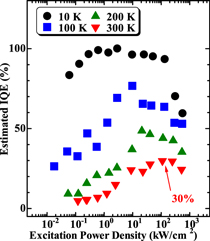
Fig. 1. (Color online) EPD dependence of the estimated IQE at 10, 100, 200, and 300 K for the Alx Ga1−x N-based UV-A MQWs. Reproduced from H. Murotani, H. Miyoshi, R. Takeda, H. Nakao, M. Ajmal Khan, N. Maeda, M. Jo, H. Hirayama, and Y. Yamada, J. Appl. Phys. 128, 105704 (2020); DOI: 10.1063/5.0015554, with the permission of AIP Publishing.
Download figure:
Standard image High-resolution imageAt lower EPDs, the estimated IQE increased as EPD was increased, even at 10 K, indicating that nonradiative recombination occurred, even at lower temperatures. The increase in IQE at lower EPDs reflected the filling of NRCs by photogenerated excitons. Conversely, at higher EPDs, the estimated IQE decreased as EPD was increased at all temperatures, which is called efficiency droop. Various mechanisms of efficiency droop have been proposed, 44–52) but its cause remains unknown and there is currently no analytical model for this phenomenon. However, efficiency droop had only a small effect on the analysis of the initial IQE increase.
3.2. Rate equation analysis of IQE curves
A rate equation model based on the radiative and nonradiative recombination processes of excitons was used to analyze the efficiency curves. 39,40,53) The model assumes that the NRCs are saturated if they capture enough excitons and that the probability of radiative recombination is independent of the exciton density. The temporal evolution of exciton density in the model is described by the following rate equations:


Here, n is the density of the photogenerated excitons, N is the density of the excitons captured by NRCs, and D is the total density of NRCs.  is the radiative recombination rate of excitons,
  is the nonradiative recombination rate of excitons at NRCs, and
  is the capture rate of excitons by NRCs. G is the generation rate of excitons. Solving these equations in the steady state, the IQE
  is described as

where  is the PL intensity. Furthermore,
  and
and  are the fitting parameters, where
  is a constant determined by the LEE of the samples and the detection efficiency of the experimental equipment. Therefore, parameters
  and
and  are scaled by the PL intensity.
The estimated IQE was plotted against the spectrally integrated photoluminescence (SIPL) intensity to analyze the IQE curves using Eq. (3). Figure 2 shows the SIPL intensity dependence of the estimated IQE at 10, 100, 200, and 300 K for the UV-A MQWs. The SIPL intensity was normalized so that the SIPL intensity divided by the EPD (units of kW cm−2) was 100 when the estimated IQE was 100%. The fits obtained using Eq. (3) (solid lines) described the low-intensity side (below a SIPL intensity of 102) of the estimated IQE curves well at all temperatures. These results demonstrated that the increase in IQE at low carrier densities arises from the filling of NRCs. Furthermore, at 10 K, the fits agreed well with the experimental data up to the estimated IQE curve peak, indicating that at 10 K, the maximum value of IQE reached almost 100%.
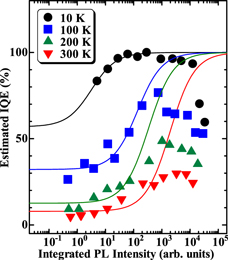
Fig. 2. (Color online) Estimated IQE at 10, 100, 200, and 300 K for the Alx Ga1−x N-based UV-A MQWs versus SIPL intensity. The solid lines show the fitting results obtained using Eq. (3). Reproduced from H. Murotani, H. Miyoshi, R. Takeda, H. Nakao, M. Ajmal Khan, N. Maeda, M. Jo, H. Hirayama, and Y. Yamada, J. Appl. Phys. 128, 105704 (2020); DOI: 10.1063/5.0015554, with the permission of AIP Publishing.
Download figure:
Standard image High-resolution imageParameters  and
and  as a function of temperature were obtained from the fitting analysis. Figure 3(a) shows the temperature dependence of parameter
  This parameter increased with temperature, demonstrating that the nonradiative recombination probability at NRCs,
  increased with temperature; thus, the nonradiative recombination of excitons at NRCs was thermally activated.
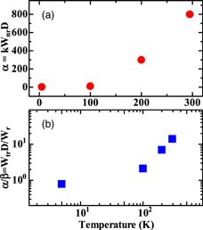
Fig. 3. (Color online) Temperature dependence of (a) parameter  and (b) parameter ratio
  for the Alx
Ga1−x
N-based UV-A MQWs. Reproduced from H. Murotani, H. Miyoshi, R. Takeda, H. Nakao, M. Ajmal Khan, N. Maeda, M. Jo, H. Hirayama, and Y. Yamada, J. Appl. Phys.
128, 105704 (2020); DOI: 10.1063/5.0015554, with the permission of AIP Publishing.
for the Alx
Ga1−x
N-based UV-A MQWs. Reproduced from H. Murotani, H. Miyoshi, R. Takeda, H. Nakao, M. Ajmal Khan, N. Maeda, M. Jo, H. Hirayama, and Y. Yamada, J. Appl. Phys.
128, 105704 (2020); DOI: 10.1063/5.0015554, with the permission of AIP Publishing.
Download figure:
Standard image High-resolution imageBecause parameter  is a function of probabilities
 and
and  we could not evaluate the temperature dependence of these probabilities based on the temperature dependence of parameter
  alone. Consequently, ratio
  was evaluated as a function of temperature. Figure 3(b) shows the temperature dependence of ratio
  The ratio increased slightly with temperature below 100 K and increased rapidly above 100 K. Similar behavior has been observed in Inx
Ga1−x
N-based systems and is caused by exciton delocalization.
39,40) It is predicted that when the excitons are localized at potential minima, where the excitons are assumed to be confined to a zero-dimensional potential, the radiative recombination probability,
The ratio increased slightly with temperature below 100 K and increased rapidly above 100 K. Similar behavior has been observed in Inx
Ga1−x
N-based systems and is caused by exciton delocalization.
39,40) It is predicted that when the excitons are localized at potential minima, where the excitons are assumed to be confined to a zero-dimensional potential, the radiative recombination probability,  is independent of temperature.
54) In contrast, the radiative recombination lifetime,
is independent of temperature.
54) In contrast, the radiative recombination lifetime,  of extended excitons in two-dimensional systems is expected to increase linearly with temperature.
54–56) The rapid increase in
of extended excitons in two-dimensional systems is expected to increase linearly with temperature.
54–56) The rapid increase in  above 100 K therefore primarily reflected the decrease in
  caused by the delocalization of excitons with increasing temperature.
The small increase in  below 100 K was explained by the increase in probability
  which was the product of the capture cross-section of NRCs and the thermal velocity of excitons, and we expected that the capture cross-section would be independent of temperature. Thus, the increase in the thermal velocity of excitons caused the small increase in
3.3. Radiative and nonradiative recombination lifetimes
Figure 4 shows PL lifetimes plotted against temperature for the UV-A MQWs at excitation energy densities (EEDs) of 0.002, 0.02, 0.2, and 2 μJ cm−2. We obtained the PL lifetimes by fitting the double-exponential function,  to the PL decay profile, which was not well fitted with a single exponential function (inset in Fig. 4). The PL intensity of the faster decay component decayed more than one order of magnitude; thus, we estimated that the PL lifetime was the faster decay time of the double-exponential function (
 ). At all EEDs, the PL lifetime decreased as temperature was increased. The time and spectrally integrated photoluminescence (TIPL) intensity decreased as the temperature was increased, which corresponded to the decrease in IQE (
 ) with increasing temperature. Because the PL lifetime (
 ) and the nonradiative recombination lifetime (
 ) are related as
  57,58) we can see that the decrease in the PL lifetime was caused by the decrease in the nonradiative recombination lifetime.
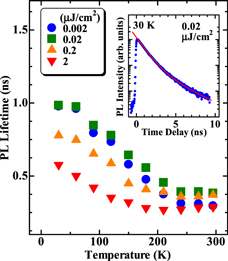
Fig. 4. (Color online) Temperature dependence of PL lifetime for the Alx Ga1−x N-based UV-A MQWs at EEDs of 0.002, 0.02, 0.2, and 2 μJ cm−2. The inset shows the PL decay curve at 30 K and an EED of 0.02 μJ cm−2. The solid line in the inset shows the fitting results using a double exponential function. Reproduced from H. Murotani, H. Miyoshi, R. Takeda, H. Nakao, M. Ajmal Khan, N. Maeda, M. Jo, H. Hirayama, and Y. Yamada, J. Appl. Phys. 128, 105704 (2020); DOI: 10.1063/5.0015554, with the permission of AIP Publishing.
Download figure:
Standard image High-resolution imageThe temperature dependence of radiative and nonradiative recombination dynamics are evaluated by estimating the radiative and nonradiative recombination lifetimes from the temperature dependence of the TIPL intensity and PL lifetime. The radiative and nonradiative recombination lifetimes are  and
and  respectively.
57,58) The IQE was obtained by a method similar to that in Sect. 3.1. The PL efficiency was defined as the TIPL intensity divided by the corresponding EED, and we assumed that the maximum PL efficiency at 10 K was 100% of the IQE. Thus, the IQE at 10 K was estimated to be 100% at an EED of 0.02 μJ cm−2.
respectively.
57,58) The IQE was obtained by a method similar to that in Sect. 3.1. The PL efficiency was defined as the TIPL intensity divided by the corresponding EED, and we assumed that the maximum PL efficiency at 10 K was 100% of the IQE. Thus, the IQE at 10 K was estimated to be 100% at an EED of 0.02 μJ cm−2.
The temperature dependence of the radiative recombination lifetime at EEDs of 0.002, 0.02, 0.2, and 2 μJ cm−2 is shown in Fig. 5(a). Below about 100 K, the radiative recombination lifetime was independent of temperature at all EEDs. The temperature-independence of the radiative recombination lifetime is a characteristic of localized (zero-dimensional) excitons.
54) Thus, these results showed that the majority of excitons were localized below 100 K. At temperatures above 100 K, the radiative recombination lifetime at all the EEDs increased with temperature almost linearly  Because this linear increase is characteristic of extended (two-dimensional) excitons,
54–56) the excitons became increasingly delocalized as the temperature was increased above 100 K.
Because this linear increase is characteristic of extended (two-dimensional) excitons,
54–56) the excitons became increasingly delocalized as the temperature was increased above 100 K.
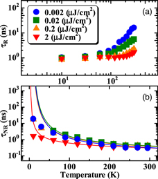
Fig. 5. (Color online) Temperature dependence of (a) radiative and (b) nonradiative recombination lifetimes (τR and τNR, respectively) for the Alx Ga1−x N-based UV-A MQWs at EEDs of 0.002, 0.02, 0.2, and 2 μJ cm−2. The solid lines in (b) show the results of the fits obtained using Eq. (4). Reproduced from H. Murotani, H. Miyoshi, R. Takeda, H. Nakao, M. Ajmal Khan, N. Maeda, M. Jo, H. Hirayama, and Y. Yamada, J. Appl. Phys. 128, 105704 (2020); DOI: 10.1063/5.0015554, with the permission of AIP Publishing.
Download figure:
Standard image High-resolution imageThe temperature dependence of the nonradiative recombination lifetime at EEDs of 0.002, 0.02, 0.2, and 2 μJ cm−2 is shown in Fig. 5(b). The nonradiative recombination lifetime decreased monotonically with increasing temperature at all EEDs. The temperature dependence of the nonradiative recombination lifetime was analyzed by using a simple model of the nonradiative recombination process, in which NRCs capture the delocalized excitons. 34,59) In the model, the reciprocal of the nonradiative recombination lifetime is written as

where  is the capture cross-section of NRCs,
  is the thermal velocity of excitons,
  is the density of NRCs, and
  is the degree of localization at a given temperature. Because the thermal velocity is proportional to
  coefficient
  can be written as
  where
where  is a constant. Hence, the reciprocal of the nonradiative recombination lifetime is expressed by the right-hand side of Eq. (4). The results of the fit obtained using Eq. (4) are shown as solid lines in Fig. 5(b). The model described by Eq. (4) is based on the exciton delocalization process; therefore, the experimental data were fitted well at temperatures above 100 K because the excitons were assumed to be delocalized in this temperature range. The solid lines agreed well with the nonradiative recombination lifetimes measured for temperatures above 100 K at all EEDs. These results suggested that the simple model in Eq. (4) could explain the nonradiative recombination process of extended (delocalized) excitons. We interpreted the disagreement between the solid lines and the experimental data at low temperatures as reflecting the nonradiative recombination process of localized excitons. More work is required to reveal the mechanism of the nonradiative recombination process of localized excitons.
According to the fitting, parameter A was estimated to be 0.27, 0.21, 0.21, and 0.20 ns−1 K−1 at 0.002, 0.02, 0.2, and 2 μJ cm−2, respectively, and  was estimated to be 120, 120, 108, and 20 K at 0.002, 0.02, 0.2, and 2 μJ cm−2, respectively. The filling of NRCs explained the decrease in parameter A because the effective density of NRCs decreased as the density of photogenerated excitons increased. The decrease in parameter
  was also explained by the decrease in exciton localization owing to the localized states filling as the density of photogenerated excitons increased.
3.4. Comparison of  and
and


First, we discuss the temperature dependence of parameter ratio  Ratio
Ratio  represents the probability that the excitons are captured by NRCs in addition to the radiative recombination. Therefore, a ratio of less than 1 indicates that radiative recombination is dominant, whereas a ratio of more than 1 indicates that nonradiative recombination is dominant. Figure 6 shows ratio
  plotted against temperature. Open squares indicate ratio
  calculated with the rate equation. The ratio was greater than 1 at temperatures above 100 K, which showed that the nonradiative recombination process was dominant even at 100 K. To improve the IQE, it is necessary to decrease the ratio at room temperature. Consequently, the temperature dependence of
  indicated that the IQE could be increased by suppressing the decrease in the radiative recombination probability and reducing the NRC density. Thus, exciton localization should help to increase the IQE.

Fig. 6. (Color online) Temperature dependence of parameter ratio  (open squares) and parameter
  (closed symbols) for the Alx
Ga1−x
N-based UV-A MQWs. Parameter
(closed symbols) for the Alx
Ga1−x
N-based UV-A MQWs. Parameter  is obtained at EEDs of 0.002, 0.02, 0.2, and 2 μJ cm−2. Reproduced from H. Murotani, H. Miyoshi, R. Takeda, H. Nakao, M. Ajmal Khan, N. Maeda, M. Jo, H. Hirayama, and Y. Yamada, J. Appl. Phys.
128, 105704 (2020); DOI: 10.1063/5.0015554, with the permission of AIP Publishing.
is obtained at EEDs of 0.002, 0.02, 0.2, and 2 μJ cm−2. Reproduced from H. Murotani, H. Miyoshi, R. Takeda, H. Nakao, M. Ajmal Khan, N. Maeda, M. Jo, H. Hirayama, and Y. Yamada, J. Appl. Phys.
128, 105704 (2020); DOI: 10.1063/5.0015554, with the permission of AIP Publishing.
Download figure:
Standard image High-resolution imageNext, we compare the analyses of the efficiency curves and the recombination dynamics. Parameter ratio  is expressed as
  and probability
  is the product of the NRC capture cross-section and the thermal velocity of excitons. Thus, the parameter ratio
  represents the same physical quantity as parameter
  The closed symbols in Fig. 6 show the temperature dependence of parameter
  at EEDs of 0.002, 0.02, 0.2, and 2 μJ cm−2. At all EEDs, the behavior of
  agreed with that of parameter ratio
  but particularly at 0.02 μJ cm−2, at which the IQE was estimated to be 100% at low temperatures, parameter
  agreed quantitatively with
  The quantitative agreement demonstrated that the rate equation analysis based on radiative and nonradiative exciton recombination, including the filling of NRCs, was valid for Alx
Ga1−x
N-based UV-A MQWs and that exciton recombination processes should be considered when analyzing the IQE.
The quantitative agreement demonstrated that the rate equation analysis based on radiative and nonradiative exciton recombination, including the filling of NRCs, was valid for Alx
Ga1−x
N-based UV-A MQWs and that exciton recombination processes should be considered when analyzing the IQE.
Finally, we discuss the EED dependence of parameter  Parameter
  decreased as the EED was increased and this decrease was larger at higher temperatures (Fig. 6). Because parameter
  decreased only slightly from 0.27 to 0.21 as the EED was increased from 0.002 to 2 μJ cm−2, the decrease in parameter
  primarily corresponded to the decrease in radiative recombination lifetime
  [Fig. 5(a)]. The decrease in
  was larger at higher temperatures, similar to the decrease in
  In other words, the increase in EED slowed the increase in
  with temperature. Because the increase in
  was caused by the exciton delocalization, the exciton delocalization was suppressed with increasing exciton density. A plausible explanation for this result was that excitons were redistributed as the EED was increased. At lower EEDs, the excitons remained in the local potential minima. With increasing exciton density, the local potential minima were filled and the excitons traveled further to reach vacant localized states. Although the long-distance redistribution of excitons populated various localized states, the exciton population of the lowest localized states increased substantially because the probability of exciton delocalization from the deeper localized states was low. Therefore, the rate of exciton delocalization was predicted to decrease with increasing EED. A similar explanation has been proposed for Alx
Ga1−x
N epilayers,
60) Inx
Ga1−x
N/GaN quantum wells,
61) and InAs/AlAs quantum dots.
62)
was caused by the exciton delocalization, the exciton delocalization was suppressed with increasing exciton density. A plausible explanation for this result was that excitons were redistributed as the EED was increased. At lower EEDs, the excitons remained in the local potential minima. With increasing exciton density, the local potential minima were filled and the excitons traveled further to reach vacant localized states. Although the long-distance redistribution of excitons populated various localized states, the exciton population of the lowest localized states increased substantially because the probability of exciton delocalization from the deeper localized states was low. Therefore, the rate of exciton delocalization was predicted to decrease with increasing EED. A similar explanation has been proposed for Alx
Ga1−x
N epilayers,
60) Inx
Ga1−x
N/GaN quantum wells,
61) and InAs/AlAs quantum dots.
62)
3.5. IQE at higher temperatures up to 750 K
In the following section, we assess the optical properties of UV-C MQWs. Figure 7 shows the temperature dependence of the PL spectra for the UV-C1 MQWs at an EPD of 60 kW cm−2. The PL spectra were measured with a back-scattering configuration. At 10 K, the PL peak from the well layers was observed around 283 nm. The PL peak at about 266 nm arose from the emission from the barrier layer and/or OCL. The wavelength of both PL peaks shifted toward the longer-wavelength side as the temperature was increased. The Bose–Einstein expression describes the temperature dependence of the PL peak wavelength; 63) thus, the PL redshift should reflect the temperature-dependent decrease of the bandgap. Even at 750 K, a clear PL peak from the well layers was visible around 295 nm.
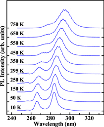
Fig. 7. (Color online) Temperature dependence of the PL spectra for the Alx Ga1−x N-based UV-C1 MQWs at an EPD of 60 kW cm−2. Reproduced from H. Murotani, R. Tanabe, K. Hisanaga, A. Hamada, K. Beppu, N. Maeda, M. Ajmal Khan, M. Jo, H. Hirayama, and Y. Yamada, Appl. Phys. Lett. 117, 162106 (2020); DOI: 10.1063/5.0027697, with the permission of AIP Publishing.
Download figure:
Standard image High-resolution imageWe evaluated the IQE to investigate the thermal stability of the radiative recombination process. Figure 8 shows the temperature dependence of the estimated IQE for the UV-C1 MQWs as a function of EPD. The estimated IQE was normalized to the maximum value at 10 K. The estimated IQEs from 10 to 300 K and from 300 to 750 K were measured using different cryostats and calibrated with values measured at 300 K. To prevent sample damage, the PL was not measured from 350 to 750 K at higher EPDs. At all temperatures, the estimated IQE increased and subsequently decreased as the EPD was increased. The initial increase in IQE at 10 K showed that the nonradiative recombination process occurred even at 10 K. However, at lower EPDs, the efficiency curve remained almost unchanged between 10 and 50 K, suggesting that the majority of nonradiative recombination pathways were inactive below 50 K. Hence, the assumption that the maximum estimated IQE at 10 K was almost 100% was also appropriate.
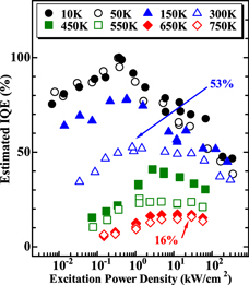
Fig. 8. (Color online) EPD dependence of the estimated IQE from 10 to 750 K for the Alx Ga1−x N-based UV-C1 MQWs. The maximum IQE was estimated to be 53% at 300 K and 16% at 750 K. Reproduced from H. Murotani, R. Tanabe, K. Hisanaga, A. Hamada, K. Beppu, N. Maeda, M. Ajmal Khan, M. Jo, H. Hirayama, and Y. Yamada, Appl. Phys. Lett. 117, 162106 (2020); DOI: 10.1063/5.0027697, with the permission of AIP Publishing.
Download figure:
Standard image High-resolution imageThe maximum IQE was estimated as 53% at 300 K and 16% at 750 K (Fig. 8). The well-resolved PL spectrum and the high IQE at 750 K showed that the radiative recombination was effective even at 750 K, which demonstrated that the radiative recombination probability was high and nonradiative recombination was well-suppressed. Thus, the excitonic optical transition was dominant in the radiative recombination, even at 750 K, owing to the stability of the excitons in Alx Ga1−x N-based UV-C MQWs at these high temperatures. 22,64)
3.6. STE characteristics
Figure 9 shows the EPD dependence of the PL spectra for UV-C1 MQWs at (a) 10 and (b) 295 K in the edge-emission configuration. Even though the edge-emission configuration was used, the PL signal was collected from the sample surface as well as from the sample edge. At lower EPDs, only spontaneous emission (SPE) with interference ripples was observed at both temperatures. As the EPD was increased, the narrow line from the STE appeared at the shorter-wavelength side of the SPE at both temperatures, and the estimated PL peak wavelengths of the STE were 277 nm at 10 K and 274 nm at 295 K. Figures 9(c) and 9(d) show the EPD dependence of the integrated PL intensity at 10 and 295 K, respectively. At both temperatures, the integrated PL intensity increased linearly as the EPD was increased to the threshold EPD (Pth), whereas above Pth, the integrated PL intensity increased superlinearly with the EPD. The superlinear increase in the integrated PL intensity supported our attribution of the narrow line to the STE. Thus, we estimated the threshold EPD for STE to be approximately 13 kW cm−2 at 10 K and 69 kW cm−2 at 295 K.
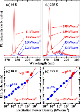
Fig. 9. (Color online) EPD dependence of PL spectra at (a) 10 and (b) 295 K, and integrated PL intensity (IPL) at (c) 10 and (d) 295 K for the Alx Ga1−x N-based UV-C1 MQWs in the edge-emission configuration. The threshold EPD for STE was estimated to be 13 kW cm−2 at 10 K and 69 kW cm−2 at 295 K. Reproduced from H. Murotani, R. Tanabe, K. Hisanaga, A. Hamada, K. Beppu, N. Maeda, M. Ajmal Khan, M. Jo, H. Hirayama, and Y. Yamada, Appl. Phys. Lett. 117, 162106 (2020); DOI: 10.1063/5.0027697, with the permission of AIP Publishing.
Download figure:
Standard image High-resolution imageFigure 10(a) shows the temperature dependence of the threshold EPD for STE. The increase in threshold EPD with increasing temperature was small from 10 to 200 K and from 250 to 295 K, whereas the increase was rapid between 200 and 250 K. The threshold EPDs were 32 kW cm−2 at 200 K and 59 kW cm−2 at 250 K. The temperature dependence of the peak wavelength for the STE spectra around the threshold EPD is shown in Fig. 10(b). Although the peak wavelength remained almost constant as the temperature was increased from 10 to 200 K, the PL peak wavelength shifted suddenly at the same time as the rapid increase in the threshold EPD occurred between 200 and 250 K. Thus, we focused on the STE spectra near the threshold EPD. Figures 11(a) and 11(b) show the PL spectra near the threshold EPDs at 250 and 200 K, respectively. The PL spectrum at 200 K (blue line) contained a narrow peak, whereas the PL spectrum at 250 K (red line) contained a broad peak. The difference in the STE spectra reflected the change in the shape of the optical gain spectrum between 200 and 250 K. These results indicated that the STE mechanism changed between 200 and 250 K.

Fig. 10. (Color online) Temperature dependence of (a) threshold EPD for STE (Pth) and (b) peak wavelength of the STE spectrum around the threshold EPD for the Alx Ga1−x N-based UV-C1 MQWs. Reproduced from H. Murotani, R. Tanabe, K. Hisanaga, A. Hamada, K. Beppu, N. Maeda, M. Ajmal Khan, M. Jo, H. Hirayama, and Y. Yamada, Appl. Phys. Lett. 117, 162106 (2020); DOI: 10.1063/5.0027697, with the permission of AIP Publishing.
Download figure:
Standard image High-resolution image
Fig. 11. (Color online) EPD dependence of PL spectra at (a) 250 and (b) 200 K for the Alx Ga1−x N-based UV-C1 MQWs around the threshold EPD for STE. A narrow line was observed for STE at 200 K, whereas a broad peak was observed at 250 K. Reproduced from H. Murotani, R. Tanabe, K. Hisanaga, A. Hamada, K. Beppu, N. Maeda, M. Ajmal Khan, M. Jo, H. Hirayama, and Y. Yamada, Appl. Phys. Lett. 117, 162106 (2020); DOI: 10.1063/5.0027697, with the permission of AIP Publishing.
Download figure:
Standard image High-resolution imageTo determine the mechanism of the STE as a function of temperature, we estimated the Mott transition density of excitons. The Mott transition density for Al0.45Ga0.55N was estimated as  ∼ 3 × 1018 cm−3, from
  where
where  is the exciton Bohr radius and
  is a dimensionless quantity. To estimate the Mott transition density,
  was estimated by linear interpolation between the effective masses of electrons and holes, the dielectric constant between GaN and AlN, and using
  65) The threshold EPD of 59 kW cm−2 at 250 K corresponded to a carrier density of roughly 7 × 1018 cm−3. The carrier density was estimated from the EPD assuming that the absorption coefficient was 105 cm−1 and the decay time constant was 1 ns. Thus, the threshold carrier densities for the STE at ≥250 K were more than twice the Mott transition density, whereas those at ≤200 K were less than or near the Mott transition density. The temperature dependence of the STE spectra and the threshold EPD suggested that the STE at 250 K and above resulted from degenerate EHP. Furthermore, excitonic transitions were likely involved in the STE at 200 K and below. Consequently, we proposed that between 200 and 250 K, the mechanism of optical gain formation changed from excitonic transitions to EHP.
42) It was unclear why the STE appeared at the higher-energy side of the SPE, although the exciton localization may have contributed to this behavior.
66)
65) The threshold EPD of 59 kW cm−2 at 250 K corresponded to a carrier density of roughly 7 × 1018 cm−3. The carrier density was estimated from the EPD assuming that the absorption coefficient was 105 cm−1 and the decay time constant was 1 ns. Thus, the threshold carrier densities for the STE at ≥250 K were more than twice the Mott transition density, whereas those at ≤200 K were less than or near the Mott transition density. The temperature dependence of the STE spectra and the threshold EPD suggested that the STE at 250 K and above resulted from degenerate EHP. Furthermore, excitonic transitions were likely involved in the STE at 200 K and below. Consequently, we proposed that between 200 and 250 K, the mechanism of optical gain formation changed from excitonic transitions to EHP.
42) It was unclear why the STE appeared at the higher-energy side of the SPE, although the exciton localization may have contributed to this behavior.
66)
In III-nitride semiconductors, the exciton-related mechanisms of optical gain formation have mainly been reported for GaN epilayers 67–69) and Inx Ga1−x N-based MQWs 66) and epilayers, 70) whereas excitonic STE has not been reported in Alx Ga1−x N-based systems. Even though the mechanism of optical gain formation is unknown, we demonstrated that STE occurred from excitonic processes in Alx Ga1−x N-based UV-C MQWs. The threshold carrier density of the excitonic STE was one or two orders of magnitude lower than that of the EHP-based STE. The excitonic gain should help to decrease the threshold current density of LDs.
3.7. Lowering the threshold carrier density by structural optimization
In Sects. 3.7 and 3.8, we report the results of our latest experiments. Recently, we performed optically pumped STE measurements for a UV-C2 MQW that had an optimally positioned quantum well region. The UV-C2 MQW structure was sandwiched between the upper and bottom Al0.50Ga0.50N OCLs. The sample was also grown on a c-plane sapphire substrate following deposition of a 4 μm thick AlN layer and a 2 μm thick Al0.63Ga0.37N cladding layer. The MQW structure consisted of three periods of 2 nm thick Al0.32Ga0.68N well layers separated by 7 nm thick Al0.50Ga0.50N barrier layers. The thicknesses of the upper and bottom OCLs were 85 and 40 nm, respectively. All the layers were intentionally undoped.
Figure 12 shows the EPD dependence of the PL spectra at 295 K for the UV-C2 MQWs. At EPDs less than 11 kW cm−2, the SPE from the well layers dominated the spectra. The SPE had a peak wavelength around 274 nm. A narrow line corresponding to the STE emerged on the shorter-wavelength side of the SPE and increased superlinearly as the EPD was increased. The peak wavelength and linewidth of the STE were estimated to be 271.6 and 1.76 nm (29.5 meV), respectively. The integrated PL intensity increased linearly below the threshold EPD and superlinearly above the threshold EPD (inset in Fig. 12). For the STE, the threshold EPD was estimated to be 26 kW cm−2, which was about 2.6 times smaller than the threshold EPD for the UV-C1 MQWs (see Sect. 3.6).
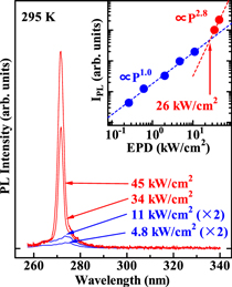
Fig. 12. (Color online) EPD dependence of PL spectra at 295 K for the Alx Ga1−x N-based UV-C2 MQWs in the edge-emission configuration. The inset shows the integrated PL intensity (IPL) versus EPD.
Download figure:
Standard image High-resolution imageFigure 13(a) shows the temperature dependence of the peak shift of the STE spectrum relative to the peak at 10 K for the UV-C2 MQWs near the threshold EPD, indicated by the closed circles. Below 200 K, the position of the STE peak varied slightly, and then shifted toward the lower-energy values as the temperature was increased further. Because the peak wavelength of the SPE exhibited a similar trend, the peak shift was attributed to the temperature-dependent decrease of the bandgap. The linewidth (FWHM) of the STE spectrum for the UV-C2 MQWs around the threshold EPD as a function of temperature is shown by the closed circles in Fig. 13(b). The linewidth of the STE broadened gradually and showed no rapid change as the temperature was increased. The temperature dependence of the peak shift and linewidth showed no major changes in the shape of the optical gain spectrum as the temperature was increased, suggesting that the mechanism of optical gain formation was unchanged as the temperature was increased to 295 K. The open squares in Figs. 13(a) and 13(b) indicate the peak shift and linewidth, respectively, of the STE spectrum for the UV-C1 MQWs. 42) A sudden blue shift and rapid broadening of the STE spectrum were observed simultaneously between 200 and 250 K, which probably reflected the change in the mechanism of optical gain formation from the excitonic transition process to EHP recombination between 200 and 250 K. Therefore, the temperature dependence of the peak shift and linewidth for the UV-C2 MQWs suggested that excitonic processes contributed to the optical gain formation up to room temperature.
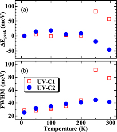
Fig. 13. (Color online) Temperature dependence of the (a) peak shift and (b) linewidth of the STE around the threshold EPD. The closed circles indicate the peak shift and the linewidth for the Alx Ga1−x N-based UV-C2 MQWs. The open squares indicate the data for the Alx Ga1−x N-based UV-C1 MQWs.
Download figure:
Standard image High-resolution imageWe examined the temperature dependence of the threshold EPD for the STE. Figure 14 shows the temperature dependence of the threshold EPD and threshold carrier density for the STE for the UV-C2 MQWs, indicated by the closed circles. At 10 K, the estimated threshold EPD was 11 kW cm−2, which was similar to the value at 10 K obtained for the UV-C1 MQWs (13 kW cm−2). As the temperature was increased, the threshold EPD showed almost no change up to 200 K and increased only slightly above 200 K. At 295 K, the threshold EPD was estimated to be 26 kW cm−2. The threshold EPDs for the UV-C1 MQWs are shown by the open squares in Fig. 14 for comparison. 42) The threshold EPD for the UV-C1 MQW increased suddenly in the temperature range of 200–250 K, which probably reflected the change in the mechanism of optical gain formation from the excitonic transition process to EHP recombination. This observation confirmed that the optical gain formation in the UV-C2 MQWs resulted from the excitonic transition process at room temperature.
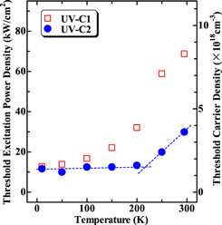
Fig. 14. (Color online) Temperature dependence of the threshold EPD and carrier density for STE. The closed circles and open squares indicate the data for the Alx Ga1−x N-based UV-C2 and UV-C1 MQWs, respectively.
Download figure:
Standard image High-resolution imageThe threshold carrier density at 295 K was estimated from the threshold EPD to be 3.6 × 1018 cm−3, which was close to the Mott transition density of approximately 3 × 1018 cm−3. The threshold carrier densities below or close to the Mott transition density indicated that the excitons were stable around the threshold carrier density, and thus the STE at room temperature was excitonic in origin for the UV-C2 MQWs.
3.8. STE at higher temperatures
Recently, we performed optically pumped STE measurements above room temperature up to 550 K for a UV-C3 MQW. The UV-C3 MQW structure was sandwiched between the upper and bottom Al0.50Ga0.50N OCLs. The sample was also grown on a c-plane sapphire substrate following deposition of a 4 μm thick AlN layer and a 2 μm thick Al0.63Ga0.37N cladding layer. The MQW structure consisted of three periods of 2 nm thick Al0.32Ga0.68N well layers separated by 7 nm thick Al0.50Ga0.50N barrier layers. The thickness of the upper and bottom OCLs was 62 nm. All the layers were intentionally undoped.
Figure 15(a) shows the EPD dependence of the PL spectra at 295 K for the UV-C3 MQWs. At EPDs of 4.5 and 11 kW cm−2, the spectra were governed by SPE from the well layers. The peak wavelength of the SPE was located around 281 nm. With increasing EPD, a narrow line due to the STE appeared at the shorter-wavelength side of the SPE peak. The peak wavelength of the STE was estimated to be 279 nm and the FWHM was estimated to be 18.5 meV. Figure 15(b) shows the EPD dependence of integrated PL intensity at 295 K. The integrated PL intensity increased linearly with EPD up to the threshold EPD, and the superlinear increase in the integrated PL intensity occurred above the threshold EPD. The threshold EPD was estimated to be 18.5 kW cm−2. According to the previous reports, the minimum value of the threshold EPD for STE was 3 kW cm−2 for Alx Ga1−x N-based UV-C MQWs on AlN bulk substrates. 71) On the other hand, the minimum value was 61 kW cm−2 on sapphire substrates. 72) Therefore, the threshold EPD of 18.5 kW cm−2 for STE is the lowest value reported to date for Alx Ga1−x N-based UV-C MQWs on sapphire substrates.
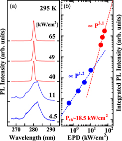
Fig. 15. (Color online) (a) EPD dependence of PL spectra at 295 K for the Alx Ga1−x N-based UV-C3 MQWs in the edge-emission configuration. (b) EPD dependence of the integrated PL intensity.
Download figure:
Standard image High-resolution imageTo evaluate the thermal stability of the formation process of optical gain, we performed temperature-dependent STE measurements. Figure 16 shows the EPD dependence of the PL spectra at (a) 400, (b) 450, (c) 500, and (d) 550 K. At each temperature, the broad SPE peak was observed at lower EPDs and the narrow line of the STE appeared on the shorter-wavelength side of the SPE peak with increasing EPD. In particular, the STE was clearly visible, even at 550 K. The separations between the STE and SPE peaks at 500 and 550 K were about twice those at 450 K and below. Figure 17(a) shows the temperature dependence of the peak energy of the STE and the SPE. The closed circles and triangles indicate the peak energies of the STE (ESTE) and the SPE (ESPE), respectively. The ESPE shifted toward the lower-energy side with increasing temperature, which reflected the temperature-dependent shrinkage of the bandgap energy. In contrast, ESTE was blue shifted with increasing temperature from 450 and 500 K. The closed squares in Fig. 17(a) show the energy separation between ESTE and ESPE as a function of temperature. Although the energy separation varied slightly, it was almost independent of temperature up to 450 K, and then increased rapidly between 450 and 500 K. Thus, the peak of the optical gain spectrum shifted suddenly with increasing temperature from 450 to 500 K. Figure 17(b) shows the FWHM of the STE peak around the threshold EPD as a function of temperature. The FWHM of the STE peak was almost unchanged with increasing temperature up to 450 K, and then the STE peak broadened above 450 K. Consequently, the optical gain spectrum broadened significantly above 450 K. These observations unambiguously indicated that the STE features changed between 450 and 500 K. Thus, the origin of STE at 500 K and above was different from that at 450 K and below, and the mechanism of the optical gain formation changed between 450 and 500 K.

Fig. 16. (Color online) EPD dependence of PL spectra at (a) 400, (b) 450, (c) 500, and (d) 550 K for the Alx Ga1−x N-based UV-C3 MQWs in the edge-emission configuration.
Download figure:
Standard image High-resolution image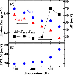
Fig. 17. (Color online) (a) Peak energy of STE (ESTE) and SPE (ESPE), and the energy separation (ΔE) between ESTE and ESPE as a function of temperature for the Alx Ga1−x N-based UV-C3 MQWs. (b) FWHM of STE spectra around the threshold EPD as a function of temperature.
Download figure:
Standard image High-resolution imageFigures 18(a) and 18(b) show the temperature dependence of the threshold EPD for STE on a linear scale and a logarithmic scale, respectively. The closed squares indicate the threshold EPD for the UV-C3 MQWs. The results for the UV-C1 and UV-C2 MQWs are also shown for comparison by closed triangles and circles, respectively. The threshold EPDs up to 500 K were estimated from the EPD dependence of the integrated PL intensity. Although the threshold EPD at 550 K could not be estimated from the integrated PL intensity, it was estimated from the spectral feature in Fig. 16(d) as between 124 and 143 kW cm−2. The threshold EPD increased slightly with increasing temperature from 295 to 450 K, and then a rapid increase occurred above 450 K [Fig. 18(a)]. We observed the rapid increase in the threshold EPD with increasing temperature above 200 K for the UV-C1 MQWs [closed triangles, Fig. 18(a)], which was explained by a change in the mechanism of optical gain formation. 42) Moreover, the slope of the threshold EPD on the logarithmic scale above 500 K was steeper than that below 450 K [Fig. 18(b)]. Because the slope of the threshold EPD depended on the thermal stability of STE, the change in the slope indicated a change in the thermal stability of the optical gain formation process and implied a change in the mechanism of the optical gain formation. Therefore, the temperature dependence of the threshold EPD supported the change in the mechanism of optical gain formation between 450 and 500 K.
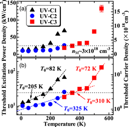
Fig. 18. (Color online) Temperature dependence of threshold EPD and carrier density for STE on (a) a linear scale and (b) a logarithmic scale for the Alx Ga1−x N-based UV-C1, UV-C2, and UV-C3 MQWs.
Download figure:
Standard image High-resolution imageTo discuss the temperature dependence of the mechanism of the optical gain formation, we calculated the Mott transition density of excitons and compared it with the estimated value of the threshold carrier density. In Figs. 18(a) and 18(b), the Mott transition density of  cm−3 for Al0.32Ga0.68N is shown by the dotted line and the right-hand y-axes indicate the threshold carrier density estimated from the threshold EPD. The threshold carrier densities at 500 and 550 K were estimated to be
  and
and  cm−3, respectively. These values were more than twice the Mott transition density. Thus, the excitonic transition processes may not contribute to the optical gain formation at 500 K and above. The optical gain formation at 500 K and above originated from the degenerate EHP. In contrast, the threshold carrier density at 450 K was estimated to be
  cm−3, and thus the threshold carrier densities at 450 K and below were close to or less than the Mott transition density. Consequently, the excitonic transition processes can contribute to the optical gain formation at 450 K and below. The exciton resonance has been observed up to 750 K in the PL excitation spectra of Alx
Ga1−x
N-based MQWs with an emission wavelength of a similar spectral range at the same EPD.
22) Therefore, the excitonic transition processes were involved with the optical gain formation at 450 K and below.
cm−3, and thus the threshold carrier densities at 450 K and below were close to or less than the Mott transition density. Consequently, the excitonic transition processes can contribute to the optical gain formation at 450 K and below. The exciton resonance has been observed up to 750 K in the PL excitation spectra of Alx
Ga1−x
N-based MQWs with an emission wavelength of a similar spectral range at the same EPD.
22) Therefore, the excitonic transition processes were involved with the optical gain formation at 450 K and below.
Next, we evaluate the thermal stability of the STE from the temperature dependence of the threshold EPD. The temperature dependence of the threshold EPD is usually analyzed by the empirical equation,  where
where  is a constant and
  is the characteristic temperature. The dashed lines in Fig. 18(b) indicate the results of fits using the empirical equation. The characteristic temperature was estimated to be
  K at 295–450 K and
  K above 450 K for the UV-C3 MQWs;
  K at 10–200 K and
  K above 200 K for the UV-C1 MQWs; and
  K at 10–295 K for the UV-C2 MQWs, which was similar to the characteristic temperature for the UV-C3 MQWs at 295–450 K. The UV-C2 MQWs had the same structure as the UV-C3 MQWs, except for the thickness of the OCLs. Thus, the origin of the STE and its thermal stability at temperatures below 295 K for the UV-C3 MQWs were expected to be similar to those of the UV-C2 MQWs. Therefore, the characteristic temperature of the UV-C3 MQWs at temperatures between 10 and 450 K was estimated to be 310–325 K. The characteristic temperature of
  K around room temperature was more than twice that reported for Alx
Ga1−x
N-based UV-A LDs.
73) The large characteristic temperature indicated the high thermal stability of the optical gain formation process. Therefore, these observations demonstrated excitonic STE with a low threshold and high thermal stability at room temperature.
K around room temperature was more than twice that reported for Alx
Ga1−x
N-based UV-A LDs.
73) The large characteristic temperature indicated the high thermal stability of the optical gain formation process. Therefore, these observations demonstrated excitonic STE with a low threshold and high thermal stability at room temperature.
Finally, we performed optically pumped lasing measurements with a high spectral resolution for the UV-C3 MQWs with a cavity length of 27 μm to confirm the lasing action due to the excitonic gain formation mechanism. Figure 19 shows the EPD of the PL spectra at 295 K. At the EPD of 11 kW cm−2, only a broad PL band of SPE was observed at approximately 281 nm. A narrow emission band with fine structures appeared at the shorter-wavelength side of the SPE with increasing EPD. The peak wavelength of the narrow band was estimated to be approximately 279 nm. The narrow band increased superlinearly with increasing EPD. The fine structures were clearly resolved at EPDs of 35 kW cm−2 and above. The separation between the structures was estimated to be approximately 0.54 nm. The longitudinal mode spacing of a Fabry–Pérot cavity is expressed as  where
where  is the cavity length and
  is an effective refractive index. The longitudinal mode spacing was estimated using
  ∼ 2.5
74,75) to be 0.58 nm for a cavity length of 27 μm and was roughly consistent with the spacing between the fine structures. Thus, the fine structure was attributed to the longitudinal cavity mode. Based on the superlinear increase in the PL intensity and the clearly resolved fine structures, the narrow band was attributed to the lasing spectra. Therefore, these observations confirmed that excitonic lasing occurred at room temperature.
∼ 2.5
74,75) to be 0.58 nm for a cavity length of 27 μm and was roughly consistent with the spacing between the fine structures. Thus, the fine structure was attributed to the longitudinal cavity mode. Based on the superlinear increase in the PL intensity and the clearly resolved fine structures, the narrow band was attributed to the lasing spectra. Therefore, these observations confirmed that excitonic lasing occurred at room temperature.

Fig. 19. (Color online) EPD dependence of PL spectra for the Alx Ga1−x N-based UV-C3 MQWs in the edge-emission configuration with a high spectral resolution. Longitudinal cavity modes are observed in the STE spectra.
Download figure:
Standard image High-resolution image
4. Conclusions
We have reviewed our recent experimental studies on Alx Ga1−x N-based UV-A and UV-C MQWs. We used PL and TRPL spectroscopy to examine the relationship between the recombination dynamics of excitons and the IQE of Alx Ga1−x N-based UV-A MQWs. Temperature- and EPD-dependent PL measurements were used to evaluate the IQE, and the dependence of IQE on excitation density was analyzed with the rate equation model for the radiative and nonradiative recombination of excitons. In addition, we measured the radiative and nonradiative recombination lifetimes by temperature-dependent TRPL, and analyzed them as functions of temperature and EED. The probability ratios of exciton capture by NRCs and the radiative recombination of excitons were measured individually by using the two above-mentioned experimental analyses. The two probability ratios agreed well, indicating that using the radiative and nonradiative recombination processes of excitons, which included the process of filling NRCs, to analyze Alx Ga1−x N-based UV-A MQWs was valid. We also studied the STE properties of Alx Ga1−x N-based UV-C MQWs grown on c-plane sapphire substrates with a high IQE of 53% at 300 K and 16% at 750 K. The optically pumped STE was clearly visible up to room temperature. We estimated the threshold EPD to be 13 kW cm−2 at 10 K and 69 kW cm−2 at 295 K. The temperature dependence of the threshold EPD for the STE and the peak wavelength of the STE spectra suggested that the optical gain formation mechanism changed from excitonic to degenerate EHP in origin between 200 and 250 K. Furthermore, based on our latest experiments, we have demonstrated a lower threshold for STE by optimizing the position of the quantum well region using OCLs, and a threshold EPD of 18.5 kW cm−2 at 295 K was achieved, which is the lowest value for Alx Ga1−x N-based UV-C MQWs grown on sapphire substrates. The lower threshold indicated that the optical gain formation was excitonic in origin up to 450 K. Our results may expand the potential use of Alx Ga1−x N-based MQWs to improve the performance of deep-UV light-emitting devices.
Acknowledgments
The authors would like to thank the graduate students in their laboratories, who have dedicated themselves to this research. This work was partially supported by JSPS KAKENHI Grant Nos. JP16H04335, JP16H06428, and JP20K04585 and by the New Energy and Industrial Technology Development Organization (NEDO), Japan.
Biographies

Yoichi Yamada was born in Yamaguchi, Japan, in 1965. He received the B.E. and M.E. degrees in electrical engineering from Osaka University, Osaka, Japan, in 1988 and 1990, respectively. He received a Ph.D. degree in physics from the University of Tsukuba, Ibaraki, Japan, in 1993. After he worked at the Institute of Physics, the University of Tsukuba as a research associate, he joined Yamaguchi University in 1995. He is currently a professor at the Department of Electrical and Electronic Engineering, Graduate School of Sciences and Technology for Innovation, Yamaguchi University. He has been working on the optical characterization of wide bandgap semiconductors from the viewpoint of excitonics (exciton engineering). He is a member of the Japan Society of Applied Physics (JSAP) and the Physical Society of Japan (JPS).

Hideaki Murotani was born in Hiroshima, Japan, in 1982. He received the B.E., M.E., and Ph.D. degrees in electrical and electronic engineering from Yamaguchi University, Yamaguchi, Japan, in 2005, 2007, and 2010, respectively. After he worked at the Department of Electrical and Electronic Engineering, National Institute of Technology (NIT), Toyota College, he joined NIT, Tokuyama College in 2015. He is currently an associate professor at the Department of Computer Science and Electronic Engineering, NIT, Tokuyama College. The focus of his current research is to characterize the excitonic optical properties of III-nitride semiconductors and their quantum structures. He is a member of the Japan Society of Applied Physics (JSAP) and the Institute of Electronics, Information and Communication Engineers (IEICE).

Noritoshi Maeda was born in Yamaguchi, Japan, in 1970. He received his B.E. and M. E. degrees in physics from Nagoya University, Japan, in 1993 and 1995, respectively. He received a Ph.D. degree in electrical engineering from Saitama University, Japan, in 2014. He joined RIKEN in 2009, and, currently, he is a research scientist of Quantum Optodevice Laboratory in RIKEN. He has been working on the crystal growth of AlGaN based nitride-semiconductors and the development of deep-ultraviolet light-emitting diodes (DUV-LEDs) and laser diodes (LDs). He is a member of the Japan Society of Applied Physics.

M. Ajmal Khan was born in Wana, South Waziristan, Pakistan, in 1975. He received the M.Sc and M.Phil degrees in Applied Physics from Quaid-i-Azam University, Islamabad, Pakistan, in 1998 and 2001, respectively. He received his Ph.D. degree in applied physics from the Graduate School of Pure and Applied Sciences, University of Tsukuba, in 2013. In 2012, during his Ph.D. work, he has discovered the thin film of boron (B) doped p-type BaSi2 layer "p+" along with his Ph.D. supervisor Prof. Takashi Suemasu. After his Ph.D. he joined the team of FUTUTER PV-Innovation, Japan Science and Technology Agency, Fukushima Renewable Energy AIST Institute (FREA), Koriyama. In FREA, he worked on Si NWs, c-SiGe and a-Si/c-Si heterojunction solar cells. In 2017, he moved to Prof. Hideki Hirayama Lab at Riken. He is currently a research scientist at RIKEN Cluster for Pioneering Research. Since then, he has been doing research on the epitaxial growth, characterization and device applications of group III-nitride semiconductors UV LEDs and laser diodes. He is a member of the Japan Society of Applied Physics (JSAP) and the guest editor of the MDPI Journal of Crystal.

Masafumi Jo was born in Miyazaki, Japan, in 1975. He received his Ph.D. from the University of Tokyo in 2003. After he worked at Research Institute for Electronic Science, Hokkaido University, and National Institute for Materials Science (NIMS), he joined RIKEN in 2013. He is currently a senior researcher of Quantum Optodevice Laboratory in RIKEN. He has been working on the crystal growth of semiconductors, and on the fabrication of nano-structured solid-state light sources. He is a member of the Japan Society of Applied Physics.

Hideki Hirayama was born in Ibaraki, Japan, in 1966. He received the B.E., M.E. and Ph.D. degrees in physical electronics engineering from Tokyo Institute of Technology (TIT), Japan, in 1989, 1991 and 1994, respectively. In the same year, he became a research scientist of RIKEN (the institute of physical and chemical research), Japan. He became a team leader of the Terahertz Quantum Device Team in 2005. He got a position of chief scientist and director of Quantum Optodevice Laboratory in 2012. He took on a concurrent position as visiting professor at Saitama University, Tokyo University of Science and Tokushima University in 2004, 2017 and 2019, respectively. His research focuses on crystal growth of AlGaN based nitride-semiconductors and the development of deep-ultraviolet light-emitting diodes (DUV-LEDs) and laser diodes (LDs). He is also developing terahertz quantum cascade lasers (THz-QCLs) based on intersub-band optical transition of semiconductor quantum cascade structures. He won a Young Scientist Award of the Minister of Education, Culture, Science and Technology in 2005, a Japan IBM Science Prize in Electronics in 2010, an Ichimura Science Prize in 2011, a Science and Technology Award of the Minister of Education, Culture, Science and Technology in 2014, a Compound Semiconductor Electronics Achievement Award (Isamu Akasaki Award) of the Japan Society of Applied Physics (JSAP) in 2019, etc. He is a member of the Japan Society of Applied Physics (JSAP), the Institute of Electronics, Information and Communication Engineering (IEICE), the Laser Society of Japan, the Institute of Electrical Engineers of Japan (IEEJ). He is a JSAP fellow. He is currently a Chief Executive Editor of JJAP/APEX.