
Abstract
Orienting semiconducting polymers (SCPs) using solution-processable techniques for organic electronic devices is essential for realizing a printable electronics device. Preparation of oriented films on liquid substrates and transferring on actual device substrate offers many advantages, including layer-by-layer coating, independent control of morphology, freedom to choose substrates, and device geometry. The floating films transfer method (FTM) has emerged as a unique method to prepare oriented films of SCP using solution processing. Here, we review recent progress in this method from the viewpoint of improvement in FTM to orient SCPs and their anisotropy in organic field effect transistors. In addition, the use of FTM films in sensing applications is also reviewed.
Export citation and abstract BibTeX RIS
1. Introduction
Semiconducting polymers (SCPs) have gained appreciable attention in the past three decades for their potential applications in gas sensors, phototransistors, and wearable organic circuits. 1–6) Morphologies of organic thin films have proven to be crucial for organic electronics devices. 7–9) SCPs are quasi-one-dimensional in nature and possess extended π-conjugation along their backbone, resulting in relatively high carrier mobility in the main chain direction. Due to this, orienting polymers uniaxially in their films is one of the most effective fabrication strategies to improve the charge transport along the orientation direction in planar devices such as organic field-effect transistors (OFETs). Macromolecular orientation has a history of more than three decades, and several methods have been developed to achieve this goal. 10) These methods can be broadly categorized by mechanism causing orientation and have been reviewed in detail in the recent past. 5,11–14) Anisotropy in charge transport due to uniaxial orientation, is also of interest for realizing the dense arrays of devices in circuits with less parasitic current, such as adjacent transistor channels orientated orthogonally in staggered thin films for p-channel and n-channel OFETs.
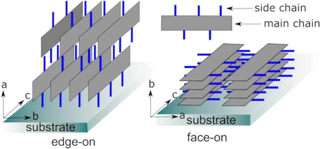
Morphological requirements in out-of-plane devices such as organic solar cells have already been reviewed by many researchers in detail. 15,16) Therefore, in this review, charge transport-related discussions will be mainly limited to planar devices such as field-effect transistors. In general, SCPs adopt two types of orientations, like edge-on and face-on in their thin films, as shown in Fig. 1, which are responsible for controlling the anisotropy and overall field-effect mobility. 17) However, charge transport anisotropy and overall field-effect mobility in some new classes of donor-acceptor-based SCPs are not limited by conventional theory and charge transport mechanisms are a bit different, as reported by others. 18) Orientation of SCPs in thin films and their length scales are of major concern for practical applications such that conformation of long axis (c-axis) and π–π stacking (b-axis) are measured with respect to the substrate plane. However, for practical application, orientation/conformation is crucial for device performance, and length scale of such orientation is important for realizing the dense array of devices on large areas. 19,20)

Fig. 1. (Color online) Schematic representation of orientation in SCPs.
Download figure:
Standard image High-resolution imageDifferent methods to orient SCPs using mechanical shear forces and solution processable methods possess several limitations reported in detail. 17,19,21) Considering the fabrication of super flexible organic circuits with SCPs using roll-to-roll processing or printing compatible techniques, various challenges need to be resolved, such as (i) film fabrication on soft flexible substrates, (ii) use of polymeric dielectrics involving hydrophobic interfaces, and (iii) availability of orthogonal solvents for staggered heterostructures. Film fabrication with polymer solution often deteriorates the organic gate dielectrics even with orthogonal solvent. 22,23) Transferring pre-fabricated solid film onto the substrate offers superior OFET performance. From the application perspective, the majority of reported orientation techniques to resolve the above challenges exist, although they are quite limited. The floating film transfer method (FTM), developed a decade ago by Kaneto and coworkers, seems to have many potential advantages. 24) This progress review will cover the progress made in recent years with focus from the viewpoint of improvement in FTM to orient SCPs and their anisotropy in OFETs. In addition, the use of FTM films in sensing applications is also reviewed.
2. Floating film transfer method
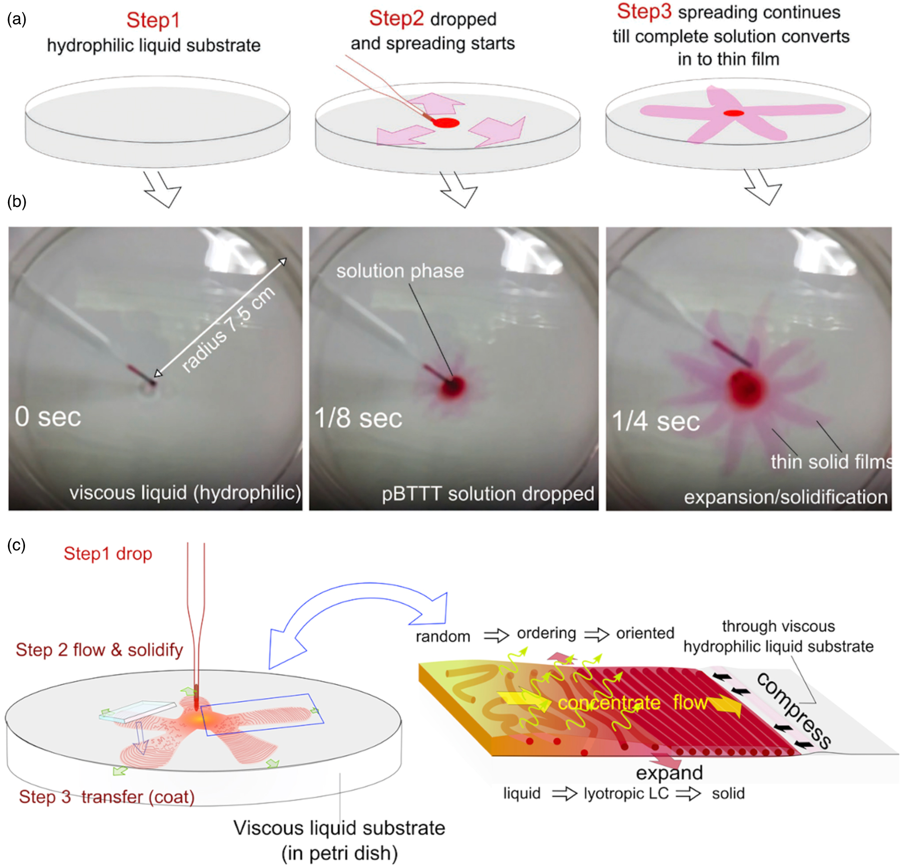
FTM was first reported by Kaneto and coworkers, where thin films are grown on orthogonal (viscous) liquid substrate and solidified floating films are then transferred on desired solid/flexible substrate. FTM and the Langmuir–Schaefer technique look similar, however controlling the surface pressure to make a compact film on the liquid surface is not needed. 24) The steps in this method are (1) placing a drop (around 10 μl) of the polymer solution in the center of the petri-dish containing an orthogonal liquid substrate, (2) allowing the polymer solution to spread followed by solvent evaporation and (3) transferring the dried floating film onto any desired substrate by stamping. A schematic representation of the film processing in a petri-dish is illustrated in Fig. 2. For liquid substrate, hydrophilic water, ethylene glycol, and glycerol are frequently chosen owing to their orthogonality with respect to commonly used hydrophobic solvents used for dissolving SCPs. Depending on the optimization, a mixture of these hydrophilic liquid substrates is often used to tune the viscosity of liquid substrates. In general, viscosity values of resulting mixtures are not mentioned because they are just used to optimize dichroic ratio (DR), and even a slight variation in viscosity makes noticeable changes in orientation intensity. The viscosity of different liquid substrates and their mixtures can be experimentally obtained and through calculations using the double-logarithmic equation of Refutas. 25,26)

Fig. 2. (Color online) (a) Schematic illustration of the steps with (b) photographs of the processes involved during film formation. Reproduced from Ref. 27. Copyright 2018, John Wiley & Sons. (c) Schematic illustration of floating film transfer method and associated possible mechanism for orientation in FTM. Reproduced from Ref. 17. Copyright 2019, Royal Society of Chemistry.
Download figure:
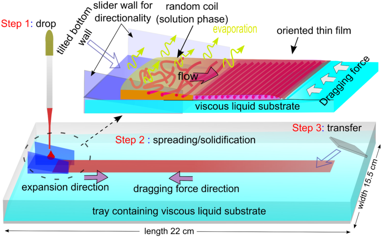
Standard image High-resolution imageIt is important to note that the fabrication of large-area and uniformly orientated thin films is highly desired for practical applications. FTM film preparations in a petri-dish, here-in-after are referred to as conventional FTM (CFTM), are suitable for prototype devices with small substrates. However, this is not that suitable as the orientation was circular considering the fabrication of large-area films as described by Pandey et al. 28) To improve this technique, we modified this technique to prepare large-area ribbon-shaped films of SCPs with uniform orientation, here-in-after referred to as unidirectional FTM (UFTM). 29) A schematic illustration of the UFTM is shown in Fig. 3. A custom-made slider of polytetrafluoroethylene sheets with side walls was employed to allow the polymer films to expand in one direction in a rectangular tray containing the liquid substrate. When the 10–20 μl of polymer solution is dropped at the junction of slider's bottom surface and liquid substrate, the slope of the slider allows film growth in the forward direction and the presence of side walls prevents the spreading of film in other directions resulting in large-area uniformly oriented ribbon-shaped floating films. Polarized UV–vis–NIR absorption spectroscopy is commonly used to quantitatively estimate orientation intensity in terms of the DR. 26) Out-of-plane and in-plane grazing incidence X-ray diffractions (GIXD) are measured to know the crystallite orientation. 27,30)

Fig. 3. (Color online) Schematic illustration of UFTM. Reproduced from Ref. 29.
Download figure:
Standard image High-resolution image3. Film preparation and orientation control in FTM
Film preparation in FTM is quite easy and can be used for different applications even if anisotropy or DR is not a major concern. This method is cost-effective, and grown films are highly uniform. However, focusing on the fabrication of macroscopically oriented films, we have found that the orientation intensity of SCPs in FTM (CFTM or UFTM) critically depends on the casting parameters such as temperature and viscosity of the liquid substrate and concentration of the polymer solution. It is worth mentioning that these casting parameters are not completely independent. For example, increase in temperature decreases the viscosity of liquid substrate. However, at a constant temperature in CFTM, we have shown how DR and film thickness of non-regiocontrolled P3HT change by changing liquid substrate mixtures combinations, as shown in Fig. 4. The three different liquid substrates used in FTM are distilled water (Wt), ethylene glycol (Eg), and glycerol (Gl), and their standard viscosity at 30 °C is 0.79, 14.41, and 487.64 centistokes, respectively. 31–33) This reflects the advantages of tuning the viscosity to optimize the DR and thickness. 34) Moreover, an increase in the viscosity decreases the expansion speed of the film and concomitantly the length of the film, resulting in an increase in the film thickness. These two phenomena are similar in CFTM or UFTM. Depending on the nature of polymer crystallization, solubility, and molecular weight, film characteristics change, therefore, tuning the concentration is required. However, we have found that the majority of the SCPs can be used within concentrations ranging from 0.5% to 2% (w/w) to optimize the DR. We have also reported that SCP concentration and temperature of liquid substrate must be tuned to obtain highly oriented film. 26,29,35)

Fig. 4. (Color online) Evolution of DR and film thickness of NR-P3HT with different liquid-substrates mixtures. Reproduced from Ref. 17. Copyright 2019, Royal Society of Chemistry.
Download figure:
Standard image High-resolution imageDuring film expansion in FTM, the viscosity of the liquid substrate is critical in imparting macromolecular orientation by providing optimal interfacial friction and compressive force, as shown in Fig. 2. Liu et al. reported film fabrication of different SCPs on low viscosity liquids, i.e. water, which generally does not induce compressive force. In comparison to spin-coated thin films, the self-assembly of SCPs and the repulsive force between their alkyl side chains and the liquid substrate results in a more crystalline film exhibiting higher mobility. 36) In addition, their film fabrication was carried out with 50 μl of dilute polymer concentration ≪ 0.1% (w/w). With such a dilute concentration in low boiling point (BP) solvent chloroform, the film solidification process takes several minutes. As a result, no macroscopic alignments are found; instead, film growth mechanisms are similar to those reported using high BP solvent. 37) Contrary to this, under FTM, the film solidification speed is fast, with solidification/expansion taking place simultaneously on the liquid substrate in seconds, as shown in Fig. 2. It was observed that appropriate control of the casting conditions, such as liquid substrate viscosity and temperature, polymer concentration and solvent mixture, meant that high orientation in large areas that extend up to many centimeters could be obtained.
4. Orientation characteristics and device performances
In the first report on CFTM, regioregular poly(3-hexylthiophene) RR-P3HT floating films were prepared. Compared to spin-coated devices, the field-effect mobility of CFTM films was increased by an order of magnitude due to high crystallinity. Although there was no evidence of macroscopic orientation in RR-P3HT, polymer domains with well-stretched polymer chains standing on the substrate with π–π stacking in the substrate plane (edge-on) were clearly demonstrated. Low film conductivity in the off-state of OFETs confirmed the absence of any contamination caused by liquid substrate components during film preparation. 24) Later, this method was reported by many different research groups to orient a variety of SCPs for organic electronic devices. 22,26,27,35,38–47)
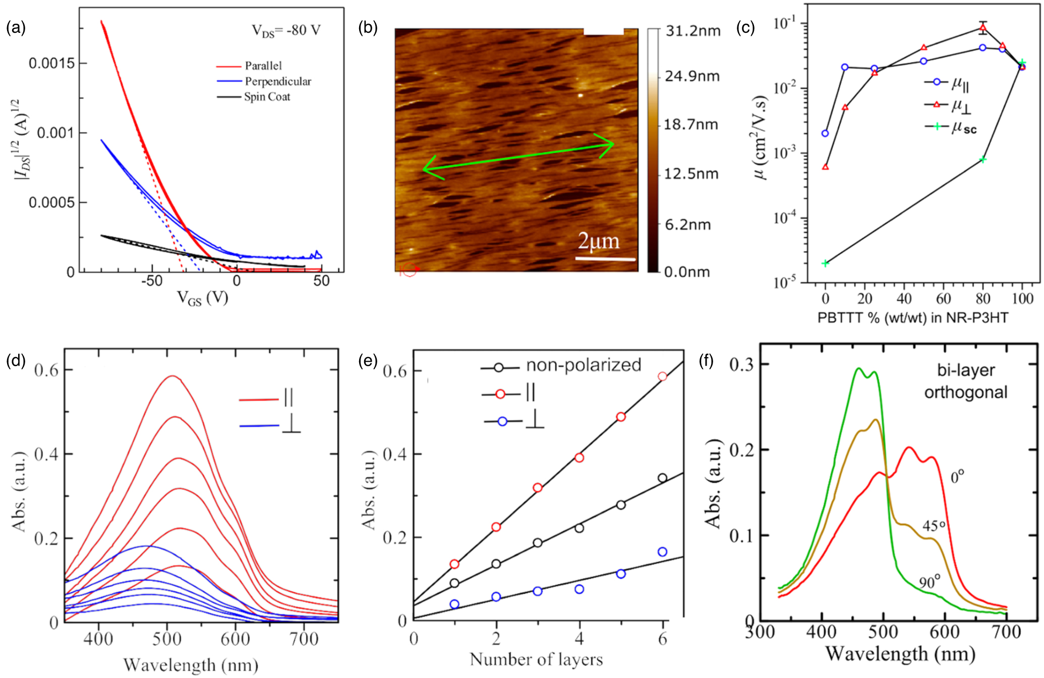
Using C-FTM, we have found that even non-regiocontrolled P3HT (NR-P3HT) with considerably low regioregularity (<80%) shows high orientation with drastic improvement in their film crystallinity and field-effect mobility in comparison to spin-coated films. 35,39) Films consisted of edge-on oriented domains with fiber-like structures along the orientation direction. In general, NR-P3HT has a poor regioregularity of around 80%, and its spin-coated films are amorphous in nature, giving field-effect mobility in the order of 10−5 cm2 V−1 s−1. The field-effect mobility of CFTM films of NR-P3HT enhanced by ∼2 orders of magnitude with charge transport anisotropy (μ∣∣/μ⊥) ∼ 5, as shown in Fig. 5. Microscopic characterizations revealed the formation of oriented fiber-like domains of NR-P3HT in CFTM films. 35) Later, these NR-P3HT films were blended with semicrystalline poly[2,5-bis(3-tetradecylthiophen-2-yl)thieno[3,2-b]thiophene] (PBTTT), resulting in a synergistic enhancement of field-effect mobility and DR. 48) Nawaz et al. have also shown excellent field-effect mobility of 8 cm2 V−1 s−1 in RR-P3HT with 100% regioregularity. 46) Nawaz et al. have also shown an improvement in field-effect mobility up to 1.3 cm2 V−1 s−1 for PDPP-TNT floating films. 22) It is worth mentioning that with cross-linked poly(vinyl alcohol) as the gate dielectric with spin-coating of PDPP-TNT, transistor characteristics were deteriorated because of interaction between SCP and the dielectric at the interface. Similar results with DPPT-TT as SCP and PMMA as the gate dielectric were reported by Sung et al. 23) However, with the same dielectrics and SCP, they obtained excellent properties with FTM films.

Fig. 5. (Color online) (a) Transfer curves of NR-P3HT prepared with different channel configurations. Reproduced from Ref. 35. Copyright 2016, Elsevier. (b) AFM image of oriented NR-P3HT film prepared by C-FTM. Reproduced from Ref. 39, Copyright 2017, Elsevier. (c) Evolution of field-effect mobility along the parallel and perpendicular direction in OFETs prepared from blending mixture of NR-P3HT and PBTTT prepared by FTM. Reprinted with permission from Ref. 48. Copyright 2020 American Chemical Society. (d) Evolution of polarized absorption spectra with multi-layer coated NR-P3HT and (e) peak height of the corresponding polarized absorption with an increase in the number of layers. (f) Polarized absorption spectra orthogonally coated F8T2 and PQT by CFTM. Reproduced from Ref. 39, Copyright 2017, Elsevier.
Download figure:
Standard image High-resolution imageOne of the special features of FTM technique is layer-by-layer coating of SCPs, which is essentially important to fabricate heterostructures using solution processing. Utilizing this feature, floating films of same or different SCPs can be easily coated without affecting the morphology of the underlying layers. As shown in Fig. 5, layer-by-layer coated NR-P3HT film (oriented ∣∣ to each other) having a similar DR is demonstrated. Notably, the DR in FTM has a critical dependence on viscosity and polymer concentration, therefore, thickness can be easily controlled using this method. Due to macroscopic orientation, we have also demonstrated that two different SCPs, poly(3,3'''-dialkylquaterthiophene) (PQT) and poly9,9-dioctyl-fluorene-co-bithiophene (F8T2) can be coated in orthogonal orientation as shown in Fig. 5. These results demonstrate that the DR can be well preserved in underlying layers, and that the number of layers can be increased in order to obtain the desired thickness. Strong vibronic modes of absorption spectra of these individual polymers coated in orthogonal direction were retained, indicating the absence of any interference in the layer-by-layer coating.
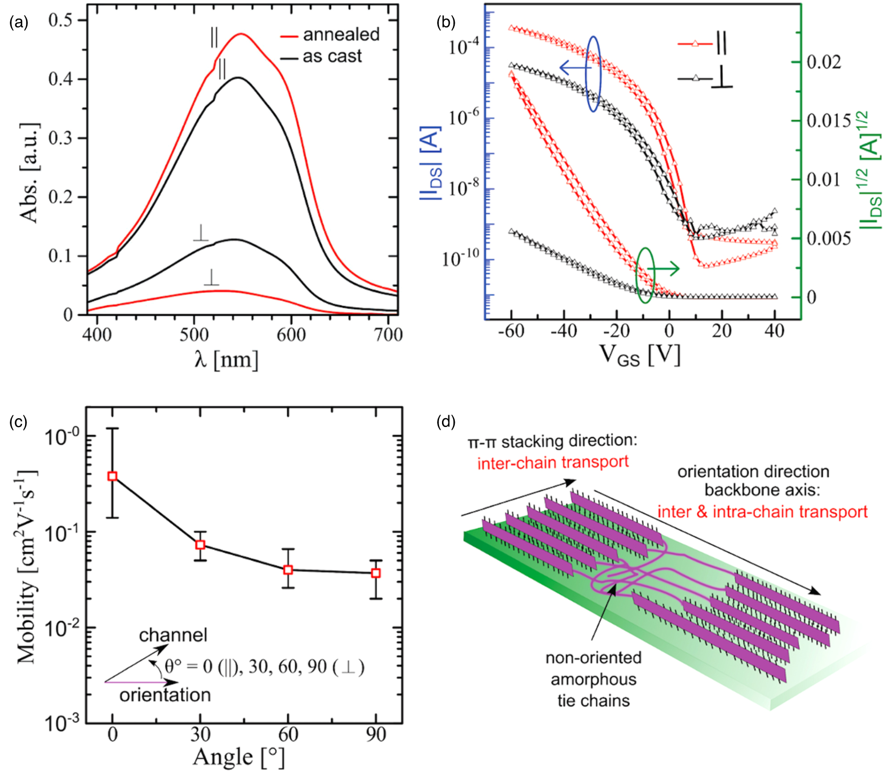
CFTM has also been applied to rigid rod-like liquid crystalline SCP, PBTTT, where DR of the as-cast FTM films was found to be in the range of 3.2–4 reaching up to 6. 27,37) DR of PBTTT films was further enhanced by annealing the films above their LC temperature, where polymer side chain melts, as shown in Fig. 6. 49) GIXD results of PBTTT coated by CFTM showed edge-on orientation with high crystallinity than those of reported values by different coating methods. The maximum field-effect mobility along the orientation direction reached up to 1.24 cm2 V−1 s−1 and was enhanced by an order of magnitude compared to the corresponding spin-coated reference samples, as shown in Fig. 6. The angle-dependent field-effect mobility drops by 6 times even when the channel direction was at 30° with respect to polymer orientation direction as shown in Fig. 6, reflecting the importance of high orientation as charge transport in SCPs is dominated by intrachain transport and assisted by tie-chains as well as π–π stacking as illustrated in Fig. 6.

Fig. 6. (Color online) (a) Polarized absorption spectra of PBTTT films prepared by C-FTM. (b) Transfer characteristics of oriented PBTTT films coated by C-FTM with channel parallel and perpendicular to the polymer orientation direction. (c) Variation of the field-effect mobility at different angles with respect to the orientation direction. (d) Schematic illustration showing the possible charge transport pathway in edge-on oriented crystallites. (Reproduced from Ref. 27. Copyright 2018, John Wiley & Sons.)
Download figure:
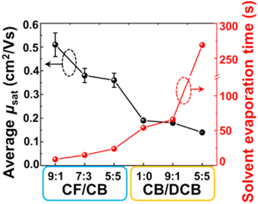
Standard image High-resolution imageWe have also demonstrated that characteristic differences of C-FTM film of SCPs prepared with low and high BP solvents 37). It was found that low BP solvent i.e. chloroform should be preferred over other solvents with high BPs like chlorobenzene or 1,2 dichlorobenzene. Solvent with low BP tends to evaporate fast during the expansion of the film on the liquid substrate. We speculate that it is important that local ordering must be assisted through lyotropic LC behavior. Although, our initial investigation revealed that SCPs with inherent LC behavior exhibit high molecular orientation in FTM films; therefore, their orientation must be getting governed by lyotropic LC phase phase-assisted self-assembly during rapid solvent evaporation and dragging forces acting in the direction opposite to film spreading due to viscosity of the liquid substrate. 47) Despite the fact that high BP solvent induces self-assembly and gives more time to form larger crystalline domains in SCPs, 8) complete replacement of low BP solvent with high BP solvent impacts the macroscopic chain alignment in FTM. 37) Later, Yang et al. demonstrated precise control of the solvent composition using high BP solvent as an additive to allow adequate time for polymer chains to self-assemble in CFTM. 42) They found that with high DR and field-effect mobility in CP1-P, high BP solvent 1,2-dicholrobenzene (DCB) was utilized as an additive to chloroform in the CFTM. Later, Sung et al., has also demonstrated that for poly[2,5-(2-octyldodecyl)-3,6-diketopyrrolopyrrole-alt-5,5-(2,5-di(thien-2-yl)thieno[3,2-b]thiophene)] (DPPT-TT), addition of a mixture of chlorobenzene and chloroform (1:10) gives high-field effect mobility with CFTM, conducted with water as liquid substrate, as shown in Fig. 7. 23) However, neither reported any macroscopic alignment in terms of DR nor performance with pure chloroform.
Recently, we have extensively worked on UFTM for improving the quality of fabricated thin films in order to achieve more reproducible films with high orientation uniformity in a large area. 29) We have also demonstrated the versatility of these UFTM films to prepare large-area (>2 cm × 15 cm) oriented thin films along with the investigation of anisotropic charge transport. 29) We also demonstrated that oriented films of a variety of SCPs could be prepared dependent on molecular weight on the DR, field-effect mobility, and charge transport anisotropy. 50,51)

Fig. 7. (Color online) Average saturation field-effect mobility and solvent evaporation times as a function of the solvent blend ratio. Reprinted with permission from Ref. 23. Copyright 2020 American Chemical Society.
Download figure:
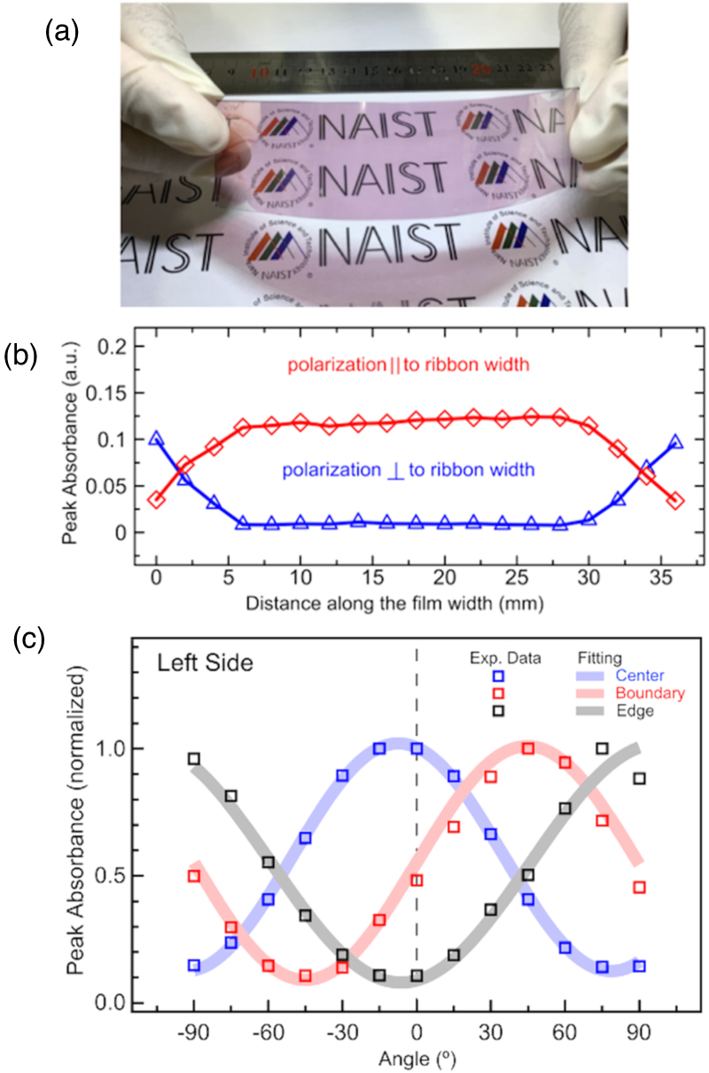
Standard image High-resolution imageIn our recent work to examine the versatility for UFTM films for large-area flexible electronics, we prepared >40 cm2 of oriented films, as shown in Fig. 8. 52) Films were found to be highly oriented, and orientation characteristics reveal that films were highly oriented along the width of the ribbon-shaped film, covering >70% of the area. Angle-dependent absorbance measurements indicated that most of the central area (70% of the film's width), had extremely consistent orientation features. The polymer's orientation direction around the edges was found to be almost orthogonal to that found in the center, as shown in Fig. 8. Angle-dependent field-effect mobilities were found to be in good agreement with orientation analysis, and the field-effect mobility of spin-coated devices was in between 0° and 90°. 52)

Fig. 8. (Color online) (a) Photograph of the uniaxially oriented films of PQT 40 cm2 on flexible PEN substrate. (b) Peak absorption intensity distribution of the film with light polarization direction parallel and perpendicular to the substrate. (c) Normalized peak intensity of angle-dependent spectra taken in different regions for the left side of the film with 0° set parallel to orientation direction in the center region of the film. Reproduced from Ref. 52. Copyright [2021] American Chemical Society.
Download figure:
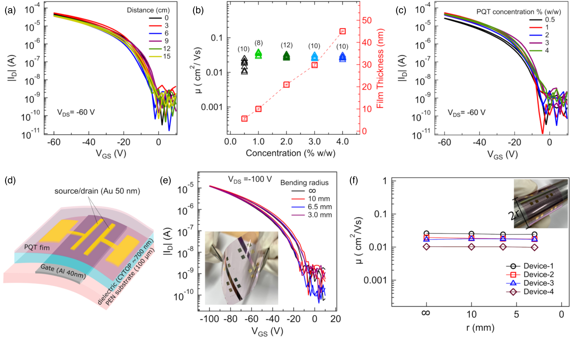
Standard image High-resolution imageThese highly oriented films resulted in the charge-transport anisotropy of 8.9. An array of OFETs fabricated with bottom-gated top-contact (BGTC) architecture along the length of single large-area (≈15 × 2.5 cm2) thin films demonstrated a very narrow standard deviation in field-effect mobility. It was found that even 2–3 layers (about 5.5 nm) edge-on oriented films, were able to create sufficient transport pathways, giving field-effect mobility in the same order as that of films with high thickness. Field-effect mobility values were found to be highly reproducible, even when the film thickness was a mere 10 nm, as shown in Fig. 9. Microstructural characterization of the thus prepared large-area thin films revealed that surface roughness of the films was within 1 nm and polymer backbones were edge-on oriented on the substrate, which is highly desirable for polymer-based OFETs. The average field-effect mobility of flexible OFETs with bottom-gated geometry on PEN substrates with CYTOP dielectrics was 0.0181 cm2 V−1 s−1, with no substantial change in mobility after bending the flexible devices at different radii (10, 6.5, and 3 mm).

Fig. 9. (Color online) (a) Transfer characteristics of OFETs prepared along the length of the ribbon in single PQT films prepared by UFTM film. (b) Evolution of field-effect mobility and film thickness with PQT concentration prepared by UFTM. (c) Transfer characteristics of OFETs prepared with different PQT concentration prepared by UFTM. (d) Schematic illustration of a flexible OFET. (e) Transfer characteristics and (f) field-effect mobility of flexible OFETs on bending at different radii. Reproduced from Ref. 52 Copyright [2021] American Chemical Society.
Download figure:
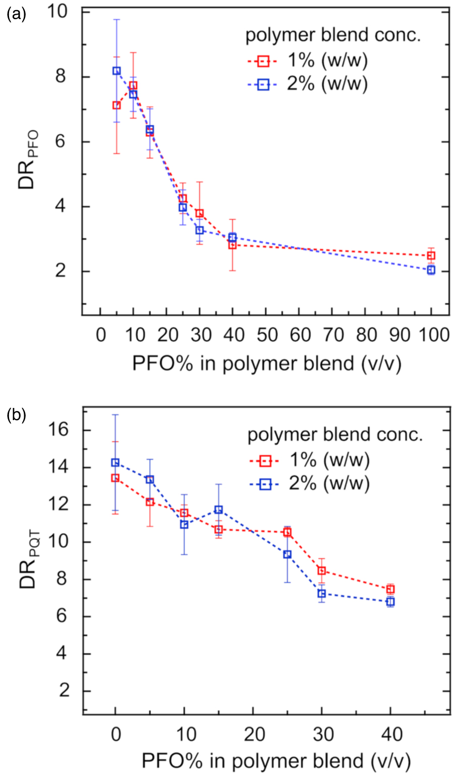
Standard image High-resolution imageRegardless of the orientation capability of different polymers, template-assisted alignment utilizing pre-patterned substrates has often been used to orient polymers. We also examined the versatility of UFTM in assisting the orientation of guest SCPs in the well-oriented host SCP matrix. Two different SCPs were blended with PQT for film preparation using UFTM, and preliminary results suggest that during film preparation, in situ orientation of guest polymers can be facilitated by blending with a host polymer. When DPPT-TT and poly(9,9-di-n-octylfluorenyl-2,7-diyl) (PFO) were blended with the host polymer PQT, the DR of both guest SCPs was increased. The DR of the host SCP decreases monotonically with an increase in the guest SCPs proportion, suggesting that guest polymers are well mixed in the host matrix without any phase separation. In addition, when the overall blend concentration was doubled to increase the film thickness, the DR of the guest polymers in the blend remained identical, as shown in Fig. 10.

Fig. 10. (Color online) Variation of DR of PFO (a) and DR of PQT (b) with increasing PFO ratio in PFO:PQT blend. Reproduced from Ref. 53. Copyright Elsevier 2021.
Download figure:
Standard image High-resolution image5. Floating films in sensing application
Photosensitive OFETs are one of the most important classes of organic electronic devices for optoelectronic applications. They play an indispensable role in image sensors, optical scanners, night vision cameras, artificial eyes, and healthcare monitoring. 54–57) P. H. Wobkenberg et al. fabricated devices with Squarilium dye and showed high NIR sensitivity. 58) In this context, the hybrid bulk heterojunction based organic phototransistors fabricated by Xu et al. demonstrated a high photosensitivity of 104. 59) However, these structures were later found to affect the overall homogeneity of the films and are thereby difficult to reproduce. We demonstrated that P3HT-based OFET prepared using FTM outperformed their spin-coated counterpart. We reported a photosensitivity of ∼104 in OFETs consisting of P3HT active layers prepared by CFTM. 60) We have also achieved a high photo responsivity of 11.3 A W−1 using PQT-based OTFT prepared by CFTM. 61) Recently, we have reported a high photosensitivity in OFETs consisting of active layers of low band gap D-A type copolymers viz. poly[2,6-[4,4-bis-(2-eth-ylhexyl)-4H-cyclopenta[2,1-b;3,4-b']dithiophene)-alt-4,7-(2,1,3-benzo thiadiazole)] (PCPDTBT) and poly(2,7-(9,9-dioctylfluorene)-alt-5,5-(4 0,7 0-di-2-thienylbenzo [c] 1,2,5) thiadiazole)] (PFO-DBT) using UFTM thin films. 40,41) We have successfully employed the orientation of SCPs for realization of high sensitivity OFETs. The orientation of SCPs was optimized to achieve high DR, as shown in Fig. 11(a), pointing towards a greater extent of anisotropy in films prepared using UFTM. Photosensitivity OFETs with a channel direction parallel and perpendicular to the polymer orientation were prepared. To evaluate the performance of these OFETs against light stimulus, OFETs were illuminated with a 630 nm red light source having intensity of 0.4 mW cm−2 and I–V characteristics were measured under dark and illumination as shown in Fig. 11(b). It was observed that the photocurrent generated upon light illumination was two orders of magnitude higher when channel direction was parallel to the orientation direction compared to that of the perpendicularly oriented one.

Fig. 11. (Color online) (a) Dichroic ratio of poly[2,6-(4,4-bis-(2-eth- ylhexyl)-4H-cyclopenta[2,1-b;3,4-b']dithiophene)-alt-4,7-(2,1,3-benzothiadiazole)] at various liquid substrate mixtures. (b) Transfer characteristics under dark and illuminated conditions with OFET channels parallel and perpendicular to polymer orientation direction. (c) Photosensitivity and responsivity as a function of gate source bias, VGS for parallel and perpendicular OFETs. (d) Modified TLM plot of W/L normalized total resistance as a function of inverse of channel length (1/L) with channel parallel and perpendicular to the polymer orientation direction. Band energy diagram showing Au-polymer interface for (e) perpendicular and (f) parallel oriented OFETs. Reproduced from Ref. 41, Copyright Elsevier 2021.
Download figure:
Standard image High-resolution imageA plot of photosensitivity, P = (IDS,On − IDS,Off)/IDS,Off, and responsivity, R = (IDS,On – IDS,Off)/PIN, against the gate to source voltage VGS is shown in Fig. 11(c). For all values of gate-source bias voltages, photosensitivity, as well as the responsivity, was found to be higher for OFETs with a channel direction parallel to the polymer orientation direction. Also, the highest values of P were observed, when the OFETs were operated in an electrically off-state (VGS > 0) owing to reduced off-state current at these gate bias voltages. An appreciable performance with a maximum P of 2 × 10⁴ and a responsivity of 17.6 A W−1 in an OFET with a channel parallel to the orientation direction was successfully demonstrated. Under both dark and illumination conditions, the on-state current of the OFETs was observed to be higher for parallel-oriented OFETs. These effects pointed towards contact-limited drive current. Using the modified transmission line method, in which the W/L is normalized to Rtotal plotted against the inverse of channel length (1/L), where L is the channel length of OFET and follows a linear dependence. 62,63) The slope of the fitting line provides an estimate of contact resistance (Rcon) present in an OFET. The Rcon in parallel and perpendicular oriented OFETs consisting of PCPDTBT active layers were estimated, as shown in Fig. 11(d). The Rcon was nearly an order of magnitude higher in the perpendicular oriented OFETs as compared to that of parallel oriented OFETs, which led to the observation of the lower on-state drive current in perpendicular oriented OFETs. 41) Improved alignment of SCPs near the metal electrodes is expected to reduce Rcon, thus yielding an improved performance OFET. In our recent work, we found a lower Rcon in P3HT coated with CFTM in comparison to spin-coated films with BGTC geometry of OFET. 64)
The absorption spectra of thin films of PCPDTBT showed red-shift of the absorption maxima (λmax) appearing around 680 and 750 nm. The peak at 750 nm is indicative of the strength of intramolecular charge transport in the film and increases with an increase in the polymer chain orientation/improved crystallinity. 41) It was implied that the oriented UFTM thin films of PCPDTBT were more ordered and crystalline. As the plane of incident light was made orthogonal to the direction of chain orientation, the peaks vanished, leading to a featureless blue-shifted λmax in the absorption spectrum that strikingly resembles amorphous thin film. This further confirmed that the energetic mismatch between the work function of Au and HOMO level of the polymer was higher in perpendicular OFETs compared to that of the parallel one, leading to higher contact resistances in perpendicular OFETs. Recently, both the PCPDTBT and PFO-DBT have been effectively employed as the active layer of OFET for the realization of phototransistors sensitive towards green and red wavelengths of the electromagnetic spectrum. For PFO-DBT OFETs, a photosensitivity of 103–104 with high photoresponsivities of 8.37 and 4.6 A W−1 were realized against the green and red-light stimuli. 40) Besides improvement in the photocurrent response of OFETs, improvement in the overall charge transport in UFTM films, as evident from their higher field-effect mobilities, can further pave the way towards the realization of fast responsive OFETs.
Furthermore, both CFTM/UFTM films being very thin means they are aptly suited for transistor applications, as these thin films of SCPs (∼10–20 nm) have very small off-state current flowing through them. This results in a higher observed photosensitivity in FTM-based OFETs compared to those fabricated using a conventional technique like spin coating. In this context, a comparison for photosensitive OFETs fabricated using different materials and techniques are shown in Table I. In future, liquid crystalline properties of the photosensitive SCPs can be tailored by making suitable changes in their molecular structure to obtain high DR. These devices also hold promise for development and integration towards the realization of OFET based inverter circuits and systems. Additionally, owing to its overall immunity towards typical problems like common solvent effects as encountered in spin coating, FTM is more robust as deposition of multiple layers one over the other can be achieved with relative ease owing to the film being stamped onto the substrate in its solid-state without affecting the morphology of the underlying layer. This again opens the gateway for vertical integration of OFETs on a single substrate.
Table I. Performance comparison of single component thin film based organic phototransistors.
| Organic semiconductor | Excitation wavelength (nm) | Excitation intensity (mW cm−2) | Mobility (cm2 V−1 s−1) | Photosensitivity | Responsivity (A W−1) | References |
|---|---|---|---|---|---|---|
| BPE-PTCDI | 635 | 14 | 0.018 | 1.85 × 10³ | 3.38 × 10− 2 | 65 |
| DPPBTSPE | 632 | 24 | 1.53 | ∼105 | ∼2 | 66 |
| P3OT | 532 | 1 | 10−3–10−4 | 102 | 1 | 67 |
| PQT-12 | 525 | 0.7 | 1.1 × 10⁻³ | 102 | 6.6 | 68 |
| P3HT | 532 | 0.4 | 7.22 × 10⁻⁴ | 104 | 10 | 60 |
| PCPDTBT | 630 | 0.4 | 00°: 3 × 10⁻³ | 00°: 2 × 10⁴ | 00°: 17.6 | 41 |
| 90°: 1 × 10⁻³ | 90°: 1.36 × 10² | 90°: 8.82 | ||||
| PFO-DBT | 522 | 0.5 | 00°: 2 × 10⁻³ | 00°: 104 | 00°: 8.37 | 40 |
| 90°: 4.7 × 10⁻⁴ | 90°: 87.6 | 90°: 2.12 |
We have also explored the application of OFETs prepared with PBTTT and PQT films by CFTM for ammonia vapor and gas sensing. The exposed ammonia vapor is chemically adsorbed at the surface and creates disordered impurities responsible for altering the HOMO/LUMO energy levels. 69) The high-quality thin films of FTM are suited for such application, as charge transport in OFETs takes place within a few layers of macromolecules near the dielectric interface. Therefore, thinner films maximize the interaction with the ammonia vapor, and ammonia vapors act like acceptors in the structured and oriented PBTTT film. 70) The electron doping is possible due to the lone pair of electrons in ammonia, which is also responsible for creating additional trap sites in PBTTT film, as schematically shown in Fig. 12(a). The trap sites for the charge carrier increase the film resistance and decrease the drain current, as shown in the transfer characteristics in Fig. 12(b). At the saturation point, the PBTTT film does not adsorb any more ammonia vapor, and the drain current gets saturated. The process of fast chemical adsorption and de-adsorption (while recovery) of ammonia vapor at the surface of FTM coated PBTTT film is responsible for the high sensing performance. The self-assembled and oriented FTM film based OFET sensor results in a very high gas response of 89.84% for the ammonia vapor. In another work, CFTM coated PQT was also used by us for the fabrication of a thin-film transistor based ammonia gas sensor. 71) The structured and oriented film of PQT has shown favorable morphology for the fast and deeper interaction with the exposed ammonia gas. CFTM offered well-structured highly oriented film with enhanced surface area resulting in more chemical adsorption sites, and as a result, increases trap density in the film. The chemical adsorption sites were very high in PQT film prepared by CFTM compared to spin-coated PQT film, as seen from the change in drain current in Fig. 12(c). We found OFET prepared with CFTM coated PQT film has a relatively higher ammonia gas response (56.4%) than spin-coated film (23.9%).

Fig. 12. (Color online) (a) Ammonia interaction mechanism at the surface of FTM coated PBTTT thin film. (b) Transfer characteristics of the transistor-based sensor fabricated by FTM coated PBTTT film with increasing concentration of ammonia vapor. Reproduced from Ref. 70, Copyright Elsevier 2017. (c) Transfer characteristics of the transistor-based sensor fabricated by FTM coated and spin-coated PQT-12 under unexposed and ammonia gas exposed condition. Reproduced from Ref. 71, Copyright Elsevier 2017.
Download figure:
Standard image High-resolution image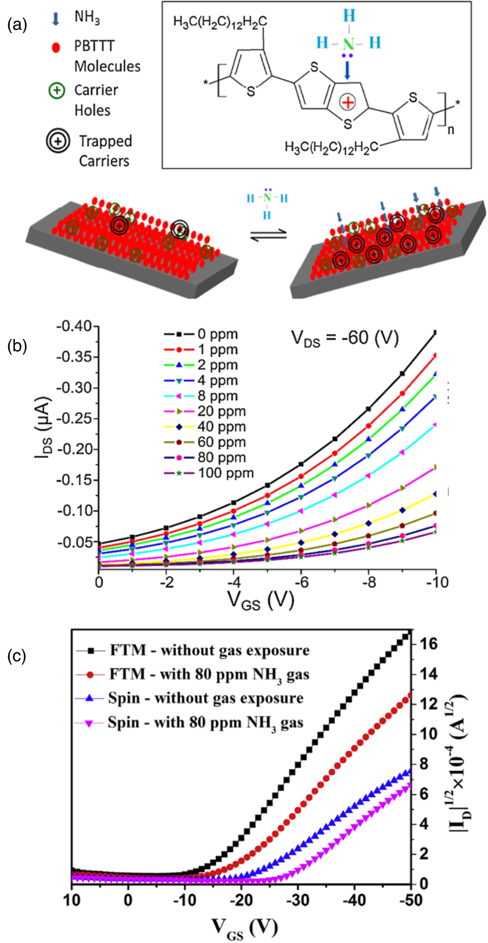
6. Conclusion
Unidirectional orientation of SCPs in their thin films is proven to be essential to improve the performance of SCP-based organic electronic devices. High intra- and intermolecular interactions resulting from the unidirectional orientation decrease the energy barriers for the charge carrier transport. As a result, high charge carrier transit through conjugated backbone is facilitated by hopping through tie-chains and π−π stacking. We have reviewed the recent progress in preparing floating films for macroscopically aligned films of SCPs for OFETs. A brief description of the casting parameter for orientation control during the film preparation is also reviewed. In addition, the importance of oriented thin films to improve the field-effect mobility and charge transport anisotropy is also highlighted. A number of techniques for the fabrication of thin films have been although reported in the literature but they have their own pros and cons, and their industrial use depends on the geometrical requirements of organic devices. However, the preparation of orientated floating films prepared on liquid substrates is emerging as an effective technique to fabricate devices with unique device architecture that are not possible with conventional methods. We strongly believe that in the near future, fully printable films by roll-to-roll fabrication of highly oriented films of SCPs, along with their application in flexible printed circuits, will be witnessed.
Acknowledgments
Part of the research presented in this review was supported by Grant-in-Aid for Scientific Research (c) (Grant Number 15K05989) and Grant-in-aid for JSPS fellows (Grant Number 20F20069) from Japan Society for the Promotion of Science. Authors are thankful to Kyushu Institute of Technology and Nara Institute of Science and Technology for providing financial support and research facilities.