
Abstract
Cu2ZnSnS4 (CZTS) is interesting as a light absorption layer for thin-film solar cells because it consists of only earth-abundant materials such as copper, zinc, tin, and sulfur. The poor adhesion between CZTS and molybdenum (Mo), which is the back metal contact material, causes CZTS to peeling off during the chemical bath deposition (CBD) for the formation of CdS as a buffer layer. This induces severe degradation of the solar cell performance. In this study, we investigated the effect of annealing following back contact metal layer formation on CZTS stability and solar cell performance. By annealing Mo/soda lime glass at 400 °C in atmosphere, Mo was oxidized, and the surface roughness of Mo increased. On the Mo surface, the CZTS peeling off was suppressed during the CBD process, resulting in an improvement in the shunt resistance.
Export citation and abstract BibTeX RIS
1. Introduction
A Cu2ZnSnS4 (CZTS) absorption layer is interesting for realizing an environmentally friendly and low-resource consumption thin-film solar cell because all its constituents—copper, zinc, tin, and sulfur—are abundant on Earth. It has a light absorption coefficient as high as 104 cm−1 and a direct transition band gap of 1.5 eV. A high energy conversion efficiency is expected based on these characteristics. 1–5) A conversion efficiency of 9.2% was reported in the case of CZTS combined with Zn0.35Cd0.65S buffer. 6) An efficiency of 11% was reported for a Cd-alloyed CZTS solar cell. 7) The highest efficiency (12.6%) was reported for CZTSSe. 8) There is still potential for enhancing the efficiency compared to the reported results, and the current performance is insufficient for practical use. Concurrently, from the viewpoint of production, a robust fabrication process is important. However, this topic has not been sufficiently studied thus far.
A typical CZTS solar cell structure consists of Al as the top contact metal, Al-doped ZnO (AZO) as the window layer, CdS as the buffer layer, CZTS as the light absorption layer, Mo as the back contact metal, and a soda lime glass (SLG) substrate. To improve the energy conversion efficiency, process optimization of each layer is required. However, good repeatability or low variation is also important for realizing a robust fabrication process. In our previous study, severe variations in the solar cell performance or CZTS peeling off were frequently observed. This was due to the poor adhesion between CZTS and Mo. The most typical behavior is the peeling off of CZTS while it is dipped in deionized (DI) water for precleaning before the chemical bath deposition (CBD) of CdS 9) or during the post-deposition annealing of CdS. The Mo surface before CZTS formation is expected to influence the CZTS/Mo interfacial adhesivity.
In this study, annealing of Mo in atmosphere was employed to modify the Mo surface, and the influence of annealing on the peeling off of CZTS and the solar cell performance was investigated. Furthermore, the influence of the post-deposition annealing temperature after CdS formation on the adhesivity improvement of the CZTS/Mo/structure was also studied.
2. Experimental methods
An SLG substrate of 5 × 5 cm2 in size was cleaned using a detergent followed by DI water cleaning with a spin dryer and ultraviolet (UV) treatment. Subsequently, an 800 nm thick Mo film was formed on the SLG by radiofrequency (RF) sputtering (200 W, 60 min, 0.4 Pa, Ar 20 sccm), and the substrate was divided to the two parts of size of 2.5 × 2.5 cm2. Following this, one sample was annealed ("post Mo annealing") in an electric muffle furnace (ADVANTEC, FUL252FA) for 45 min in atmosphere at various temperatures. The annealing temperature were 200 °C, 300 °C, and 400 °C. The temperature was monitored by the sensor installed within the muffle furnace. Another sample was not annealed to serve as a reference. The Mo surface morphology and chemical status were characterized via atomic force probe microscopy (AFM; SHIMADZU, SPM9700) and X-ray photoelectron spectroscopy (XPS; JEOL, JPS-9010MX), respectively.
On the Mo surface, a 400 nm thick CZTS precursor was formed by RF sputtering using a Cu-poor and Zn-rich sintered target control with an atomic component ratio of Cu:Zn:Sn:S = 20:16:13:51 10–12) under the sputtering conditions of 50 W, 60 min, 0.4 Pa, and Ar 20 sccm. The volume of the precursor is expanded by sulfurization, and it is considered that the volume expansion produces stress between the CZTS and Mo films. This might cause the known poor adhesion between CZTS and Mo. To decrease the volume expansion, the thickness of the precursor was tuned to be relatively thin. CZTS was formed by sulfurization of the precursor at 560 °C for 5 min in 5% diluted H2S under N2 atmospheric pressure using a hot wall furnace. X-ray diffraction (XRD; Rigaku, Miniflex) and X-ray fluorescence spectroscopy (XRF; Rigaku, ZSX mini II) were employed to investigate the crystallinity and atomic composition of the CZTS film.
The CZTS/Mo/SLG structure was soaked in DI water for 10 min to remove the metal-like secondary phase on the surface. 9) Surface photos were captures before and after the cleaning process in DI water to visually examine the CZTS peeling off phenomena. In addition, the weight reduction of the sample was checked using an electronic valance (A & D, GH202). CBD was subsequently performed to form a 70 nm thick CdS buffer layer. Post-CBD, annealing was conducted in atmosphere at 300 °C, 320 °C, 340 °C, and 360 °C for 30 min using an electric muffle furnace (ADVANTEC, FUL252FA). A 300 nm thick AZO window layer was formed by RF sputtering (150 W, 70 min, 0.5 Pa, Ar 20 sccm). A 300 nm thick Al electrode was formed by thermal evaporation using a mask for the top contact electrode. Finally, mechanical scribing was performed to isolate the solar cell with a size of 4 × 4 mm2. The current–voltage (JV) characteristics were measured using a solar simulator (JASCO, YQ-250BX) under the standard testing conditions (AM1.5 G, 100 mW cm−2, 25 °C). After the JV measurement, cross-sectional images of the solar cell were obtained by field emission scanning electron microscopy (FE-SEM; Zeiss, Ultra-55).
3. Results and discussion
3.1. Post Mo annealing
Figure 1(a) shows AFM images of the Mo surface. On the Mo surfaces without annealing and with annealing at 200 °C, a "fish-like" 13–16) structure, which is known as a typical structure of Mo, is identified. On annealing at 300 °C, the fish-like structure changes to round grains. These grains become larger, and rod and flake-like structures 17,18) are found on the Mo surface on annealing at 400 °C. This tendency contributes to the surface roughness (Ra) increase above 200 °C from ∼3 nm to 8–32 nm.
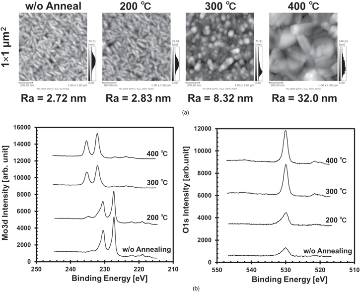
Fig. 1. Surface structure and chemical state analysis of Mo surface post Mo annealing. (a) AFM images with scan area size of 1 × 1 μm2. Ra is surface roughness. (b) Mo 3d and O 1 s XPS spectra.
Download figure:
Standard image High-resolution imageThe XPS spectra of Mo3d and O1s are shown in Fig. 1(b). The O1s XPS spectra area is significantly larger at the high annealing temperatures of 300°C and 400 °C than that at 200 °C. The Mo3d XPS spectra of the samples without annealing and with annealing at 200 °C show two strong peaks: Mo3d5/2 at 227.4 eV and Mo3d3/2 at 230.5 eV. These strong peaks have tails to a higher binding energy. Moreover, other small peaks can be observed at approximately 232 and 235 eV, which are attributed to oxidized Mo components. This oxidation is suspected to be promoted when the sample is exposed to air after Mo sputtering or annealing at 200 °C. However, the samples annealed at 300 °C and 400 °C show only two strong peaks at 232.2 and 235.4 eV, which correspond to Mo3d5/2 and Mo3d3/2. These chemically shifted spectra are consistent with the binding energy of MoO3. 19–21) These results suggest that on annealing in atmosphere above 200 °C, Mo grains grow with oxidation promotion. It is believed that the surface region detected by XPS (∼10 nm) changed from Mo to MoO3 at least.
The composition ratio of CZTS formed on the annealed Mo/SLG is shown in Fig. 2(a). No notable change is found in the composition ratio in comparison to that of the sample without annealing. Figure 2(b) shows the XRD patterns of the CZTS/Mo/SLG structures. The intensity of the diffraction peaks from CZTS112 22) normalized by Mo110 23) of the sample containing Mo annealed at 400 °C is greater than that of the other samples, as shown in Fig. 2(c). This is due to the reduction in the Mo110 diffraction peak strength. Moreover, the full width at half maximum (FWHM) of the diffraction from CZTS112 on the Mo annealed at 400 °C is broader than that obtained other the annealing conditions, even though the CZTS112 peak strength is similar in all samples. This suggests that the crystallinity of the Mo annealed at 400 °C deteriorates, and based on Scherrer's equation, 24) the grain size of the CZTS, on the Mo annealed at 400 °C is smaller than that of the other CZTS. This is supported by the in-lens SEM images shown in Fig. 3.
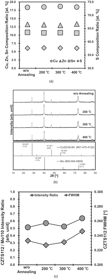
Fig. 2. Composition and crystallinity analysis of CZTS/Mo/SLG structure post Mo annealing. (a) Atomic composition ratio of CZTS obtained by XRF. (b) XRD patterns. (c) CZTS112 diffraction intensity normalized by Mo110 and FWHM of CZTS112.
Download figure:
Standard image High-resolution image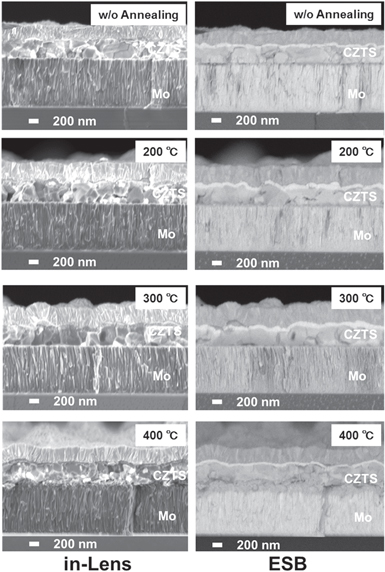
Fig. 3. Cross-sectional in-lens SEM and ESB images of stacked structure (AZO/CdS/CZTS/Mo/SLG) post Mo annealing.
Download figure:
Standard image High-resolution imageFollowing the DI water soaking as a precleaning step for the CBD, the surface was visually inspected. In this experiment, no severe peeling off of CZTS is observed in any sample. However, there is a small weight reduction of the samples without annealing and with annealing at 200 °C, as summarized in Table I. The weight of the sample was examined before and after the DI water soaking step using an electronic balance. However, weight reduction is not detected in the samples annealed at 300 °C and 400 °C. These results suggest that the annealing of Mo/SLG at 300 °C or 400 °C contributes to improving the adhesion between CZTS/Mo and suppresses even a slight peeling off of CZTS. The thermal expansion coefficients of Mo, MoO3, and CZTS are reported as 0.52 × 10⁻⁵, 1.2–5.5 × 10⁻⁵, and 1.2 × 10⁻⁵ 1 K−1, respectively. 25–27) The difference between the thermal expansion coefficients of two different material layers in contact with each other affects their adhesion. In the case of the thin MoO3 film at the interface between Mo and CZTS, the stress applied to CZTS is relaxed because the thermal expansion coefficient of MoO3 is larger than that of Mo and it is similar to or larger than that of CZTS. This may improve the adhesion between CZTS and Mo and suppress well the peeling off of CZTS.
Table I. Weights of CZTS/Mo/SLG stacked structure for 2.5 × 2.5 cm2 sample before and after DI water cleaning.
| w/o annealing | 200 °C | 300 °C | 400 °C | |
|---|---|---|---|---|
| Before [g] | 1.731 40 | 1.682 00 | 1.687 10 | 1.717 70 |
| After [g] | 1.731 30 | 1.681 90 | 1.687 10 | 1.717 70 |
| Weight reduction [g] | 0.000 10 | 0.000 10 | 0.000 00 | 0.000 00 |
Figure 3 shows cross-sectional images of the stacked structures of AZO/CdS/CZTS/Mo/SLG. In the image of the sample with annealing at 400 °C, condensation of the flake-like structure on the top of the Mo region is observed at a thickness of approximately 200 nm. This is consistent with the AFM images of the Mo surface after annealing at 400 °C. In the energy-selective back-scattered electron (ESB) images, an approximately 200 nm thick gray region is found on the top of the Mo layer. The color of the region is darker than that of the Mo bulk region. This suggests that the top of the Mo layer consists of lighter mass components than the bulk Mo. In addition, smaller grains are found at the bottom of the CZTS on the Mo annealed at 400 °C in comparison to that of the other CZTS. This results in the wider FWHM of the XRD CZTS112 peak.
The above results suggest that the annealing Mo at 400 °C in atmosphere forms an interlayer consisting of a Mo oxide flake-like structure and small grains CZTS near the Mo side.
Figures 4(a)–4(c) show the JV curves, parallel resistance (shunt resistance), and external quantum efficiency (EQE) measured using the solar simulator, respectively. The number of normally operating solar cells is increased in the samples with Mo annealing at 400 °C, as shown in Fig. 4(a). The best cell characteristics are obtained with annealing at 400 °C: η = 3.627% with open-circuit voltage (Voc) = 602.8 mV, short-circuit current density (Jsc) = 12.85 mA cm−2, fill factor FF = 0.468, series resistance (Rs) = 16.78 Ω cm2, and shunt resistance (Rsh) = 342.0 Ω cm2. The performance is clearly improved compared with that under the other conditions. In particular, the shunt resistance is significantly improved in many cells. It is presumed that the improvement in the shunt resistance between the Mo and CdS layers is induced by the suppression of the CZTS peel off by the improvement in the adhesion between CZTS and Mo, which consequently improves the cell performance. The EQE results show that there is no significant change in the shoulder drop near 500 nm and rising near 900 nm. This suggests that the band gaps of CdS and CZTS are unaffected by the annealing. However, the quantum efficiency of the solar cell with Mo annealed at 400 °C is improved in comparison to those under the other conditions, which results in the improvement in the short-circuit current.
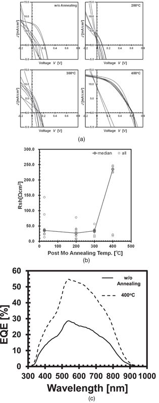
Fig. 4. Electrical characteristics of CZTS solar cells with post Mo annealing. (a) JV curves of CZTS solar cells. (b) Dependence of shunt resistance on annealing temperature. (c) EQE curves. Eight cells were formed under each condition. Cell size was 4 × 4 mm2. Measurements were performed under the standard testing conditions (AM1.5 G, 100 mW cm−2, 25 °C).
Download figure:
Standard image High-resolution imageIt is presumed that the carrier collection at Mo might be improved by the existence of the interlayer. It has been reported that MoO2 formation on Mo before CZTS formation contributes to decreasing the band bending of CZTS, which enhances the carrier collection at Mo. 28) Furthermore, the higher valence state of Mo, including MoO3, formed by UV-ozone induces a large band bending, which worsens the carrier collection. These modifications of the band bending are induced by the change in the sulfur vacancy density of MoS2, which is formed from the conversion of MoOx during sulfurization. In this study, MoO3 is formed by thermal oxidation; therefore, this process difference might affect the sulfur vacancy density.
For the sample with annealing at 300 °C, even though the Mo surface shows a larger roughness than the reference and the sample with annealing at 200 °C and a weight reduction is not detected after DI water soaking, no clear improvement, particularly in the shunt resistance, is observed in the JV characteristics. The XPS and AFM data of the sample with annealing at 300 °C show similar trends to the sample with annealing at 400 °C. However, a thick interlayer is not formed on the top of Mo, as shown in the SEM images. Although both XPS and AFM have high surface sensitivity, they cannot detect a film deeper than the escape depth of the photoelectrons. These results suggest that the improvement in the shunt resistance is realized by the formation of the thick interlayer of ∼200 nm by the annealing of Mo at 400 °C in atmosphere. A 10 nm MoOx composed of MoO3 and MoO3−x evaporated on an Mo surface was reported to increase the Na diffusion from Mo to CZTS, which resulted in grain size enlargement of CZTS, thereby improving the open circuit voltage. 29) In the present study, MoO3 formation occurs by thermal oxidation of Mo, and CZTS grain enlargement is not observed although the shunt resistance and quantum efficiency are quite improved. An in-depth investigation of the origin of this positive effect induced by MoO3 formation is still required.
3.2. Post CBD annealing
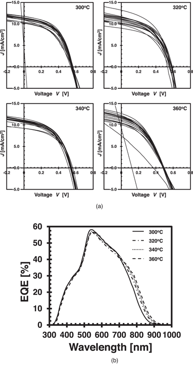
For the samples with Mo annealing at 400 °C, the post-CBD annealing temperature was changed to 300 °C, 320 °C, 340 °C, and 360 °C, and the influence of the post-CBD annealing was studied. The peeling off of CZTS was not observed in any condition.
Cross-sectional SEM observation did not show a notable difference in the distribution of the CdS layer in both in-lens SEM and ESB images.
Figures 5(a) and 5(b) show the post-CBD annealing temperature dependence of the JV characteristics and EQE, respectively. The JV characteristics show that the variation in the cells caused by the post-CBD annealing at 360 °C is large. The open-circuit voltage tends to decrease when annealed at high temperatures. This open-circuit voltage reduction worsens the efficiency at higher annealing temperatures. Based on the EQE measurement of the best cells, the band gaps of the samples annealed at 300 °C, 320 °C, 340 °C, and 360 °C, respectively, are estimated to be 1.44, 1.42, 1.41, and 1.40 eV. Thus, the bandgap becomes smaller increasing annealing temperature. Such a band gap reduction is reported in Cd-diffused CZTS. 30,31) The observed band gap reduction might be due to a small diffusion of Cd into CZTS, which is not detectable by the in-lens and ESB SEM observations.
Fig. 5. Electrical characteristics of CZTS solar cells with post CBD annealing. (a) JV curves. (b) EQE curves. Sixteen cells were formed on each substrate. Cell size was 4 × 4 mm2. Measurements were performed under the standard testing conditions (AM1.5 G, 100 mW cm−2, 25 °C).
Download figure:
Standard image High-resolution image
4. Conclusions
In this study, post-Mo annealing in atmosphere is conducted after Mo formation on an SLG substrate. After annealing at 400 °C, the Mo surface structure is changed from a fish-like structure to rod and flake-like shaped grains with the promotion of oxidation, which improves the adhesion between CZTS and Mo. This induces shunt resistance improvement and increases in the number of normally operating solar cells, and it is effective in reducing the performance variation.
For the sample with annealing at 400 °C after Mo formation, on increasing the post-CBD annealing temperature from 300 °C to 360 °C, open-circuit voltage deterioration is due to band gap reduction. In particular, at 360 °C, the variation in the JV characteristics is significant.
These results suggest that to reduce the performance variation, it is important to precisely control the entire thermal process.
Acknowledgments
This study was conducted at the Open Solution Center at the National Institute of Technology, Nagaoka College. This study was supported in part by AMADA Foundation. This study was partially supported by JSPS KAKENHI (Grant No. JP21K04142).