
Abstract
We have demonstrated an extremely low voltage rectifier by using p-GaN gate AlGaN/GaN high electron mobility transistors. In contrast to conventional GaN rectifiers, the turn-on voltage and on-state current can be decoupled, resulting in low turn-on voltage of 0.05 V and high on-state current achieved simultaneously with p-GaN designs. Furthermore, the role of p-GaN layer on current–voltage characteristics of p-GaN gated anode diode was investigated, indicating the p-GaN layer is the source of hole current. Combined the electron current with hole current, the total current was enhanced significantly with the ohmic p-GaN gate electrode. Finally, full-wave AC to DC rectification was demonstrated by a monolithically-integrated diode bridge rectifier with four p-GaN gated anode diodes. The bridge rectifier is able to operate at an input signal as low as 0.18 V, which is very promising for future power conversion applications.
Export citation and abstract BibTeX RIS
1. Introduction
With the advent of Society 5.0, energy harvesting promises to be an efficient solution to tackle the impending energy crisis. A power conversion circuit such as an AC to DC rectifier is required to convert the energy harvested in the environment into usable electrical energy. 1–6) The next-generation power rectification circuits require rectifiers with low turn-on voltage, high on-state current, and high conversion efficiency. Up to present, none of the demonstrated semiconductor diodes are able to operate at 0 V turn-on with low power loss. 7–15) Though a synchronous rectification circuit can be employed for turning on the device at 0 V, the additional power drive and increased cost offset its benefits.
AlGaN/GaN-based devices have received increasing demand for rectification applications due to their superior properties, such as high electric field, high electron saturation velocity and high electron mobility. 16) Several approaches have been proposed to implement normally-off operations, among which p-GaN gate solution has drawn great attention with a good balance between performance, reliability and manufacturing capability. 17–22) p-GaN layer lifts the potential of two-dimensional electron gas (2DEG) channel out of Fermi level, which results in a positive shift of the threshold voltage (Vth). Therefore, p-GaN design is crucial for 2DEG modulation, which allows a tailored Vth close to 0 V. Moreover, above a certain gate voltage, hole injection from p-GaN layer induces additional electrons accumulate in the 2DEG channel and thus high electron current. 23–25) Besides, p-GaN layer can be used to leverage hole current of gate p–n diode as another current path to enhance the on-state current capability. 26)
In this paper, we have demonstrated an AC–DC rectifier with extremely low turn-on voltage by using p-GaN gate AlGaN/GaN high electron mobility transistor (HEMT) in diode configuration. The anode electrode is connecting the source and gate of p-GaN HEMT and the drain of HEMT is acting as the cathode. The p-GaN layer thickness is tuned to yield nearly-zero turn-on voltage for the p-GaN gated anode diode. In addition, an ohmic p-GaN gate electrode was employed which enables a high on-state current that sums the HEMT current and the p-GaN gate to 2DEG channel current.
2. Experimental methods
The epitaxial structure consists of a buffer, an un-doped GaN, an Al0.25Ga0.75N barrier, and a 140 nm p-GaN gate with a hole concentration of 5 × 1017 cm−3 on a Si substrate. Figure 1 shows three types of devices fabricated, namely p-GaN gate HEMT, p-GaN gated anode diode and p-GaN gated anode diode bridge. For the p-GaN gate HEMT [Fig. 1(a)], devices with various p-GaN thickness were fabricated to tune the Vth close to 0 V. Based on the 0 V Vth p-GaN gate HEMT, p-GaN gated anode diodes [Fig. 1(b)] were fabricated to be able to operate as rectifiers. Furthermore, four identical p-GaN gated anode diodes were monolithically integrated to form a diode bridge for full-wave rectifications [Fig. 1(c)].
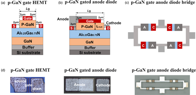
Fig. 1. (Color online) Schematic device structures of p-GaN gate HEMT (a), p-GaN gated anode diode (b), and p-GaN gated anode diode bridge with their corresponding optical microscopy images shown in (c).
Download figure:
Standard image High-resolution imageDevice processing started with the p-GaN layer etching by Cl2 (20 sccm)/BCl3 (20 sccm) based inductively coupled plasma reactive etching (ICP-RIE) with ICP and bias power of 120 and 15 W, respectively, followed by 1:1 hydrochloride acid treatment to eliminate surface damages. 22) The thickness of p-GaN after ICP-RIE was 55 nm, 45 nm, 35 nm, and 25 nm, respectively. Then, p-GaN gate mesa was patterned and etched by ICP-RIE. After that, the same ICP-RIE process was used for isolation mesa formation with a depth of 100 nm. A Ti (20 nm)/Al (20 nm)/Ti (30 nm)/Au (100 nm) metal stack was evaporated for source and drain ohmic contacts followed by thermal annealing in N2 ambient at 840 °C for 2 min. Gate contact was made on the p-GaN layer by evaporating a Ni (20 nm)/Au (20 nm) metal stack. For the ohmic gate electrode, an additional annealing process (N2 ambient at 590 °C for 2.5 min) was performed. For gated anode diodes, the anode was formed by Ti (20 nm)/Al (120 nm), followed by interconnections for the diode bridges. The top-view optical microscopy images of the three type of devices are shown in Fig. 1(d).
Current–voltage characteristics were measured using a Keithley-4200 semiconductor parameter analyzer on a Cascade Microtech MPS150 probe station. Rectification characteristics were measured by a Tektronix TBS-162 oscilloscope.
3. Results and discussion
3.1. p-GaN gate HEMT
For the fixed p-GaN doping, the variation of p-GaN thickness has a significant effect on the threshold voltage of p-GaN gate HEMT. In order to tune the Vth close to 0 V, the relation between p-GaN thickness and Vth has been studied. The thickness of p-GaN was varied between 140 and 25 nm with the p-GaN gate length fixed at 6 μm. Figure 2 shows DC characteristics measured for each p-GaN gate HEMT. Vth is extracted as a gate-to-source voltage (VGS) at the drain current density (ID) of 1 mA mm−1 at a source to drain voltage (VDS) of 5 V and plotted as a function of p-GaN thickness in Fig. 2(a). As can be seen, no change of Vth occurs until p-GaN thickness is below 55 nm. With further decreasing p-GaN thickness, Vth decreases and finally reaches negative. As the p-GaN thickness decreases, the potential of the interface between p-GaN and AlGaN decreases. Therefore, the gate bias applied to the 2DEG channel increase, which results in highly effective 2DEG modulation and therefore a reduced Vth. 27,28) In particular, for the p-GaN thickness of 35 nm, Vth as low as 0.05 V was obtained with a drain current of 100 mA mm−1 at VGS and VDS of 5 V [Fig. 2(b)]. The cross-section transmission electron microscopy (TEM) image of the 35 nm p-GaN HEMT structure is shown in the inset of Fig. 2(a) which proves the accuracy of the ICP-RIE approach. In addition, a double-peak feature is clearly observed in the transconductance (gm ) versus VGS curve. The second peak indicates conductivity modulation of 2DEG channel by the p-GaN gate layer. The onset of hole injection induces more electrons at the channel to maintain charge neutrality, and therefore results in a significant increase of the drain current, which offers a solution for high current applications. 26) It should be noted that a thin oxide layer is observed between the 2 μm long gate electrode and p-GaN by TEM, which explains the high onset voltage of hole injection due to a non-optimized ohmic contact.

Fig. 2. (Color online) Dependence of the threshold voltage on p-GaN thickness for p-GaN gate HEMTs (a) and transfer characteristics for 35 nm thick p-GaN HEMT (b). TEM cross-section image of p-GaN region for 35 nm p-GaN gate HEMT is shown in the inset of (a) (scale bar corresponds to 20 nm).
Download figure:
Standard image High-resolution imageThe reverse current–voltage (I–V) measurement was also carried out to the gate-to-drain diode with the source floating. A reverse current as low as 50 nA mm−1 was observed at the reverse bias of 200 V, which is the limit voltage of the current measurement setup.
3.2. p-GaN gated anode diode
35 nm thick p-GaN gate HEMT has exhibited an extremely low Vth and high on-state current potentials with hole injection, which is promising for low power-loss rectifiers. In this section, we demonstrate p-GaN gated anode diodes based on 35 nm thick p-GaN gate HEMT, aiming to realize low turn-on voltage and high on-state current simultaneously.
Since the forward current could benefit from the intrinsic gate p–n diode (exiting between p-GaN and 2DEG channel), we intentionally employed an elongated p-GaN layer of 54 μm to promote hole injections. Figure 3 compares I–V characteristics of p-GaN gated anode diode with different gate electrodes (Schottky and ohmic). As forward bias initially increases, devices with ohmic and Schottky electrode display identical current. When the forward bias increases above 1 V, the current of the ohmic gate device start to rise sharply, exceeding the device with Schottky gate significantly. In contrast, the Schottky gate device demonstrates a linear voltage dependent current. The additional current for the ohmic gate device is attributed to hole current which occurs when the gate p–n diode turns on. 29) For the current device, the turn-on voltage of the gate p–n diode is 1 V. It should be noted that the high reverse current of 0.2 mA mm−1 and the resulted low rectification factor of 103 (defined as the ratio of current for positive and negative voltage of 3 V) are related to the non-optimized gate ohmic contact, which can be improved by optimizing the processing conditions or employing different gate metals.

Fig. 3. (Color online) Forward current–voltage characteristics of p-GaN gated anode diodes with different gate electrodes in linear (a) and semi-log scale (b). The thickness and length of p-GaN layer is 35 nm and 54 μm, respectively.
Download figure:
Standard image High-resolution imageTo understand the contribution of the hole current to the total forward current, current components of the gated anode device were analyzed in Fig. 4. The total anode current can be decomposed into HEMT electron current (I2DEG) and gate p–n diode hole current (Ip–n diode). When a positive bias was applied to anode, 2DEG turns on at Vth, which is determined by the p-GaN layer design, and increases with the forward voltage. After the forward voltage is above 1 V, dramatic increase of total current is observed. At this point, the gate p–n diode turns on and gradually dominates the total current. Therefore, Ip–n diode could enhance the total current without affecting the turn-on voltage, i.e. high current and low turn-on voltage can be obtained simultaneously. This is superior to other normally-off HEMT approaches, where either the forward current is inversely correlated with the turn-on voltage, or the complicated processing scheme is always needed for the recess-gate to etch the recessed region down to several nanometer. 30–32) Furthermore, I–V characteristics of the ohmic gated anode diodes were compared for different p-GaN lengths (p-GaN thickness is fixed at 35 nm) in Fig. 5. As shown in Fig. 5(a), the I–V characteristics are divided into two regions, namely HEMT region and gate p–n diode region. In the HEMT region, the device with shorter p-GaN displays higher current while the opposite holds in the p–n diode region. This phenomenon can be well explained by the dominated current component in each region in Fig. 5(b). In region I, the forward current is inversely proportional to the p-GaN gate length, which is consistent with the 2DEG current of conventional HEMTs, indicating that the HEMT current from 2DEG channel dominates the total current. Besides, the p–n diode current is hardly observed. In region II, HEMT current becomes saturated. In contrast, gate p–n diode turns on and the corresponding current is proportional to the p-GaN gate length (i.e. gate area), which thus enables enhanced current for the 54 μm long p-GaN device. Therefore, the gate p–n diode is able to enhance the forward current by employing an enlonged p-GaN gate layer with an ohmic gate electrode.
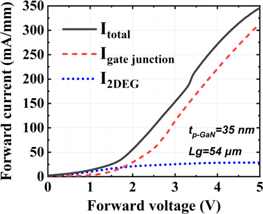
Fig. 4. (Color online) Forward current–voltage characteristics for gated anode diode with ohmic gate electrode. The thickness and length of p-GaN layer is 35 nm and 54 μm, respectively.
Download figure:
Standard image High-resolution image
Fig. 5. (Color online) Forward current–voltage characteristics for gated anode diodes with different p-GaN gate length (a) and a demonstration of the current components (b).
Download figure:
Standard image High-resolution image3.3. p-GaN gated anode diode bridge
To demonstrate the present p-GaN gated anode diode beneficial for high-efficiency rectification applications, rectification characteristics of the gated anode of with 35 nm thick and 54 μm long p-GaN was measured and demonstrated in Fig. 6. Figure 6 (a) shows the testing circuit schematic where a load of 10 kΩ was used. As seen in Fig. 6(b), half-wave rectification was achieved without any signal distortions at an AC input signal of 1.5 V. Rectification of half cycle [box in Fig. 6(b)] is magnified and shown in Fig. 6(c). Thanks to the low turn-on voltage by our p-GaN designs, nearly zero-crossing is clearly observed for the gated anode diode, i.e. even close to 0 V AC signal could be rectified which is able to reduce the power loss.
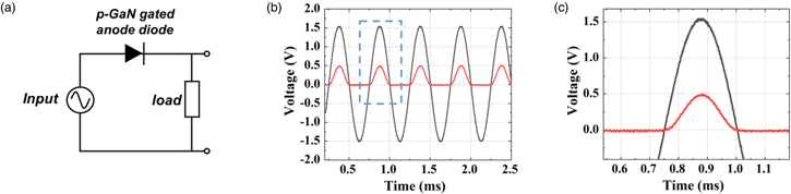
Fig. 6. (Color online) Testing circuit schematic (a) and half-wave rectification operation with a 1.5 V AC input signal for p-GaN gated anode diodes with a Vth of 0.05 V (b). The box in (b) is magnified which shows nearly 0 V crossing (c). The output signal is normalized to 1 digit.
Download figure:
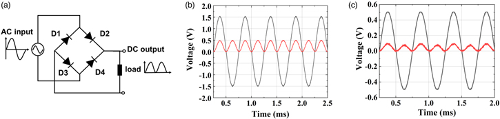
Standard image High-resolution imageTo showcase the potential of the demonstrated p-GaN gated anode diode for future rectifier applications, four of the p-GaN gated anode diodes (35 nm thick, 54 μm long) were monolithically integrated to form a full bridge rectifier. Figure 7 shows the testing circuit schematic where a load of 10 kΩ was used and the corresponding rectification characteristics. As seen in Fig. 7(b), full-wave rectification was achieved at an input signal of 1.5 V. In particular, the rectifier can operate properly at an input signal of 0.5 V as shown in Fig. 7(c), which is impossible for the current Si diodes. Furthermore, an input signal as low as 0.18 V can be rectified (not shown here). Such behavior is derived from the low turn-on voltage and high on-state current of the p-GaN gated anode diode demonstrated above. It should be noted that with further reducing the input signal, the output signal cannot be detected because of the high-level noise with the current testing setup.
Fig. 7. (Color online) Diode bridge testing circuit schematic (a) and 2 kHz full-wave rectification for the p-GaN gated anode diode bridge with an input signal of 1.5 V (b) and 0.5 V (c).
Download figure:
Standard image High-resolution image
4. Conclusions
We have demonstrated a low turn-on voltage full-wave rectifier by using p-GaN gate HEMT. Low turn-on voltage and high on-state current could be achieved simultaneously with careful p-GaN designs. With p-GaN thickness reduced to 35 nm, a threshold voltage as low as 0.05 V was obtained. Thanks to the elongated p-GaN layer design with the ohmic gate electrode, on-state current is significantly enhanced by the intrinsic gate p–n diode. In particular, the turn-on voltage and on-state current are decoupled which enables flexible designs. The diode bridge which monolithically integrated four p-GaN gated diodes exhibits excellent performance, which is able to realize full-wave rectification at an input signal as low as 0.18 V.
Acknowledgments
This work was supported by MEXT "Research and development of next-generation semiconductor to realize energy-saving society" Program Grant No. JPJ005357 and JSAP KAKENHI Grant No. JP18K18866.