

Abstract
We fabricated a Schottky barrier diode (SBD) on ion-implanted diamond substrates. The SBDs contained lightly doped regions under the Schottky electrodes and heavily doped regions beneath the Ohmic contacts. The current remained below 6.4 × 10⁻¹¹ A at reverse biases of up to 10 V, but increased sharply at a forward bias of −3.5 V. The Schottky barrier height and ideality factor under forward bias were estimated to be 1.1 eV and 10, respectively. The hole concentrations obtained by measuring the capacitance at various supplied voltages were in good agreement with the values obtained from the Hall effect measurements.
Export citation and abstract BibTeX RIS
Diamond semiconductors with an ultrawide bandgap (5.47 eV) are promising candidates for high-power and high-frequency electronic devices. These semiconductors have excellent electrical and thermal properties, such as high breakdown fields and high thermal conductivity. 1–5) Ion implantation is an effective structural optimization technique for improving the electrical performance of devices. 6) To date, diamond devices fabricated by the ion implantation technique with a CVD co-doping technique have been reported for pn junction diodes, bipolar transistors, metal insulator semiconductor field effect transistors and so on. 7–12) This technique allows the dopant atoms to be implanted at precise depths in selected areas. The performance of a laterally structured device can be optimized by doping selected areas, because regions with different dopant concentrations can be generated on the same planar substrate. Therefore, ion implantation is the most widely used doping technique for economical mass production of electronic devices based on Si substrates. Many researchers have studied the implantation of boron ions in diamond substrates. 8,13–19) The temperatures of the substrates during ion implantation can range from that of liquid nitrogen to 400 °C, and both rapid thermal annealing and furnace annealing have been investigated. 20,21) However, in spite of many attempts, there was no report on a highly efficient doping method because the defects created during ion implantation could not be removed by annealing. Seki and Nakata et al. recently reported the implantation of boron ions in highly pure freestanding (001) CVD diamond substrates and achieved an activation efficiency of 80%. 22,23) Boron ions were implanted at room temperature at fluences ranging from 5 × 1018 cm−2 to 5 × 1019 cm−2, and the doped substrates were annealed at relatively low temperatures of 1150 °C–1300 °C. The integrated circuits in diamond-based devices can also be incorporated into monolithic microwaves and smart devices for high-frequency and high-power applications. Implanting ions in specific areas is crucial for these applications.
In this study, we fabricated Schottky barrier diodes (SBDs) with planar structures by implanting boron ions into highly pure freestanding type-IIa (001) CVD diamond substrates. This diamond substrate was 3 × 3 mm2 in size and was purchased from Element Six Ltd Two different regions of the substrates were doped. Areas with high dopant concentrations formed directly beneath the Ohmic contacts, and a good linear relationship between the current and voltage was observed. The SBDs exhibited good rectification behavior at a threshold forward voltage of −3.5 V, and a small reverse current was observed up to +10 V.
A schematic cross-sectional view of a planar SBD on a type-IIa (001) CVD diamond substrate implanted with boron ions is shown in Fig. 1(a). The SBD in the figure contains two regions with different dopant concentrations. The lightly doped region formed beneath the aluminum (Al) Schottky electrode and extended to the areas below the heavily doped regions, which formed under the Ohmic electrodes. The lightly doped region exhibited good rectification behavior. The Ohmic electrodes above the heavily doped regions consisted of three layers of metals (Ti/Pt/Au).
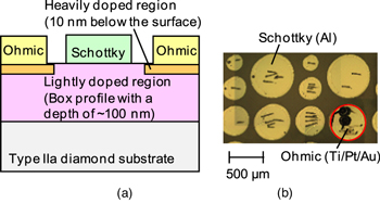
Fig. 1. (Color online) (a) Schematic cross-sectional view of the SBD structure and (b) a planar optical microscope image of a diamond SBD with heavily and lightly doped regions. The Ohmic electrode is enclosed within a red circle and the remaining electrodes are Schottky electrodes.
Download figure:
Standard image High-resolution imageThe concentration of boron ions below the Ohmic contacts was approximately 1 × 1021 cm−3, whereas the concentration in the lightly doped region was 5 × 1018 cm−3. The very low implantation energy of 5 keV to obtain the lightly doped regions significantly enhanced the Ohmic properties of the devices. The Schottky and Ohmic electrodes were in direct contact with the substrate surfaces, and the mesa etching process was not necessary for this device structure. The planar SBD structure allows for the integration of multiple devices on the same substrate.
A view of a plane of the diamond SBD obtained by optical microscopy is shown in Fig. 1(b). The Ohmic electrode is circled in red, and many Schottky electrodes of various sizes are visible. The short dark lines on the Schottky and Ohmic electrodes are the result of contact with the probe needles during the electrical measurements. The Ohmic electrode has a bump that was fabricated using ball bonders on the Ti/Pt/Au metal electrodes. The dark region on the Ohmic electrode is merely a trace of the bonding wires and does not affect the electric characteristics.
The undoped and freestanding (001) CVD diamond substrates were cleaned by subjecting them to wet treatment prior to SBD fabrication. The substrates were chemically and mechanically polished to attain an average surface roughness of 0.03 nm. After oxygen termination, 11B+ ions were implanted in multiple steps at eight different energies in the range of 5–60 keV. Implantation was performed at room temperature with ion fluences ranging from 3.5 × 1012 cm−2 to 11 × 1012 cm−2.
The boron ion depth profiles obtained by performing TRIM simulations are shown in Fig. 2. 24) The lightly doped region had a box profile with a depth of ∼100 nm and a maximum boron concentration of 5 × 1018 cm−3. A very thin region with a lower boron concentration formed approximately 10 nm below the surface.
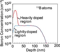
Fig. 2. (Color online) Depth profile of boron ions of the heavily and lightly B implanted regions obtained by carrying out TRIM simulations.
Download figure:
Standard image High-resolution imageAfter ion implantation, the samples were capped with 100 nm thick SiO2 layers to prevent surface graphitization during subsequent activation annealing. The samples were then annealed at 1150 °C in Ar for two hours. The SiO2 caps were removed by wet HF treatment, and additional 11B+ ions were selectively implanted beneath the Ohmic electrodes through a metal mask. Implantation was performed at a low energy of 5 keV and an ion fluence of 1.2 × 1015 cm−2, which corresponded to a maximum volumetric concentration of ∼1 × 1021 cm−3 at room temperature. The depth profile of the boron ions in the heavily doped region below the Ohmic electrodes is also shown in Fig. 2. The region with an extremely high boron concentration that formed near the diamond surface was formed using low implantation energy and a large dose of boron ions. This was expected to contribute to the formation of good Ohmic contacts with low resistivity. Another SiO2 cap was deposited on each sample after the second ion implantation step, followed by activation annealing under the same conditions used for the first annealing step. The SiO2 caps were removed via wet HF treatment, and Ohmic Ti/Pt/Au multilayers were deposited over the heavily doped regions through a metal mask. The samples were then annealed at 400 °C.
The Van der Pauw method was used to measure the Hall coefficients of the samples at temperatures ranging from 100 to 770 K. The relationship between the hole concentration and the reciprocal of the absolute temperature is plotted in Fig. 3(a). In addition, the Hall mobility is plotted as a function of the absolute temperature, as shown in Fig. 3(b). All data collected over the entire temperature range were consistent with p-type conduction. The hole concentration decreased monotonically as the reciprocal of the absolute temperature increased. The activation energy determined from the temperature-variable Hall measurements was 0.37 eV, which confirmed that the implanted B ions acted as efficient acceptor impurities. Clear evidence of hopping conduction could not be found, which indicates that the conduction of the generated holes occurred in the valence band. The hole concentration at room temperature was estimated to be 1.25 × 1013 cm−3. The Hall mobility increased as the absolute temperature decreased and reached 202 cm2 V−1 s−1 at 250 K, which is the highest level reported for ion-implanted diamond.
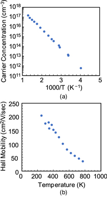
Fig. 3. (Color online) (a) Dependence of the hole concentration on the reciprocal temperature and (b) Hall mobility as a function of the absolute temperature.
Download figure:
Standard image High-resolution imageIn the final fabrication step, thermally evaporated Al was deposited on the sample surfaces through a metal mask under high vacuum to form Schottky contacts. After formation of the Al Schottky contact, the electrical properties of the SBDs were evaluated at room temperature using a B1505A power device analyzer (Keysight Technologies, USA). The current between the Ohmic contacts was plotted as a function of the supplied voltage, as shown in Fig. 4. The Ohmic contacts were 500 μm in diameter, and the centers of the two Ohmic contacts on each sample were separated by a distance of ∼2 mm. The current–voltage curves were linear across a very wide voltage range from −100 to +100 V, even though the regions located between the Ohmic contacts were lightly doped. The differential resistance was 2.3 × 10⁸ Ω at 100 V.

Fig. 4. (Color online) Current between two Ohmic contacts plotted as a function of voltage.
Download figure:
Standard image High-resolution imageThe dependence of the current on the voltage supplied to the SBDs is shown in Fig. 5. The scales of the axes in Figs. 5(a) and 5(b) are linear and logarithmic, respectively. The Al Schottky contacts were 340 μm in diameter, and each Ohmic contact was located approximately 900 μm from the center of the Schottky contact. The data shown in Fig. 5(b) indicate good rectification behavior, even though the Schottky contacts are affected by the surface properties of the doped substrates. Very little current flowed at a reverse bias, but significant current flow began at a forward bias of −3.5 V. A current of −9.4 nA was measured at a forward voltage of −7.8 V. A threshold voltage of −5.1 V was estimated by extrapolating the straight line from the point of minimum differential resistance at −8 V. As shown in Fig. 5(b), the leakage current increased above a reverse voltage of 4 V, but was less than 6.4 × 10⁻¹¹ A at a reverse voltage of 10 V. The on/off ratio of the current was 170.
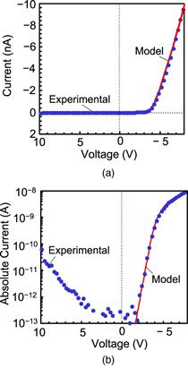
Fig. 5. (Color online) Dependence of current on the voltage supplied to diamond SBDs. (a) Current plotted as a linear function of the voltage and (b) logarithmic plot of the current as a function of the voltage.
Download figure:
Standard image High-resolution imageThe results shown in Fig. 5 were calculated using Eq. (1), according to the thermionic emission model with parasitic resistance (RS ):

where I, V, and S are the current, voltage between the Schottky and Ohmic contacts, and electrode area, respectively. ϕ B is the height of the Schottky barrier, and ns is the ideality factor. A* is the Richardson constant, q is the charge of an electron, T is the absolute temperature, and kB is the Boltzmann constant. The value of A* was assumed to be 90 A cm−2 K−2, 25) and the experimental data were in good agreement with the modeled predictions at forward bias on both the linear and logarithmic scales. The values of ϕ B , ns , and RS were calculated using the thermionic emission equation with parasitic resistance and were 1.1 eV, 10, and 3.5 × 10⁸ Ω, respectively. The large value of ns could probably be attributed to defects at the interface between the Schottky electrode and the lightly doped region, which existed to a depth of ∼10 nm below the surface and was formed during light B ion implantation.
The reciprocal of the squared capacitance (C2) at 1 kHz for a sample with a diameter of 540 μm is plotted against the supplied voltage in Fig. 6. The slope of the line decreased at approximately 4 V, and the leakage current began to increase. The hole concentration (NA ) was calculated from the slope of the line using Eq. (2)

where εS and ε0 are the semiconductor dielectric constant and permittivity of free space, respectively. The red line in Fig. 6 corresponds to the hole concentration of 1.25 × 1013 cm−3 estimated from the Hall effect measurements. At voltage sufficiently low to suppress the leakage current, the calculated hole concentrations were in good agreement with the values obtained from the Hall measurements in Fig. 3(a).

Fig. 6. (Color online) Reciprocal square of the capacitance plotted as a function of the supplied voltage.
Download figure:
Standard image High-resolution image
In this study, ion implantation was used to fabricate diamond SBDs. Undoped and highly pure (001) CVD diamond substrates were doped by implanting boron ions at room temperature, followed by activation annealing at a relatively low temperature of 1150 °C. This is the first report of the use of an all-ion-implantation process to fabricate SBDs with good rectification properties. The activation energy of 0.37 eV was determined by conducting temperature-variable Hall effect measurements. This confirmed that the implanted boron impurities acted as acceptors, and conduction of the generated holes occurred in the valence band. The SBDs contained lightly doped regions below the Schottky electrodes and heavily doped regions beneath the Ohmic contacts. The relationship of the current measured between the Ohmic contacts on an SBD and the voltage was linear. The current remained below 6.4 × 10⁻¹¹ A at reverse biases as high as 10 V, but increased sharply at a forward bias of −3.5 V. The height and ideality factor of the Schottky barrier under forward bias were estimated to be 1.1 eV and 10, respectively. The hole concentrations obtained by measuring the capacitance at various supplied voltage levels were in good agreement with the values obtained from the Hall effect measurements.
Acknowledgments
The data that support the findings of this study are available within the article