
Abstract
We present a comparative study of lateral and L-shaped PN junction Si optical phase shifters for Mach–Zehnder modulators in Si photonics based on TCAD simulation. First, we introduce an easy fabrication method for L-shaped PN junctions by inverting dominant dopant type in Si. Then, we present the quantitative comparison of Si optical phase shifters. The L-shaped PN junction device shows the larger modulation efficiency of VpiL and the lower optical phase shifter loss compared to the lateral one. The VpiL for the vertical one is 0.89 Vcm, nearly half that of the lateral one, 1.76 Vcm at the same optical phase shifter loss, 10.5 dB cm−1. Finally, taking advantage of single-drive configuration and optimizing input characteristic impedance, the large-signal simulation with 1 mW input power and a 500 μm phase shifter shows the dynamic optical modulation amplitude of 0.22 mW for the vertical one, which could be a promising solution for a compact device footprint without a traveling wave electrode.
Export citation and abstract BibTeX RIS

Content from this work may be used under the terms of the Creative Commons Attribution 4.0 license. Any further distribution of this work must maintain attribution to the author(s) and the title of the work, journal citation and DOI.
1. Introduction
Depletion-type silicon (Si) Mach–Zehnder modulators (MZM) have been mostly used as a key building block for high-performance optical interconnect systems based on Si photonics because they can provide high modulation speed and broad bandwidths which are highly attractive for cost-effective co-integration of photonics and electronics. 1–5) In particular, Si traveling wave MZMs have been actively investigated for the 200 Gb s−1 and 400 Gb s−1 IEEE Ethernet standards, taking advantage of four-level pulse amplitude modulation (PAM-4) 6) and quadrature phase shift keying (QPSK). 7)
The Si optical phase shifters on the MZMs consist of s PN junction within Si rib waveguides, where the plasma dispersion effect occurs and changes the refractive index. 8,9) In general, Si optical phase shifters based on PN junctions are classified as lateral PN junctions (LPNs) or L-shaped PN junctions (LSPNs). LPN-based optical phase shifters are the most commonly used due to their relatively easy fabrication and simple design. However, the modulation efficiency of the VpiL of Si optical phase shifters based on LPN is as high as 1.5 to 2.5 Vcm 10–13) (the modulation efficiency of an optical phase shifter is characterized by the voltage–length product of a π phase shift; therefore, a small VpiL implies high modulation efficiency). Although modulation efficiency can be reduced further by increasing free-carrier densities of the PN junction, it results in high optical loss due to free-carrier absorption. 12) In these terms, LSPN can provide larger modulation efficiency, maintaining optical loss due to the larger mode overlap between optical mode and larger junction area of LSPN compared to LPN, 14–18) but the larger junction area increases the junction capacitance, limiting the modulation speed. Although LSPN devices have been demonstrated, there have been no reports that provide a systematic and quantitative device performance comparison between LPN and LSPN optical phase shifters for the important device parameters of modulation efficiency, optical loss, and bandwidth. Therefore, it is important in the design of LSPN-based optical phase shifters to consider not only the static performance of VpiL and optical phase shifter loss but also the intrinsic RC time constant of the active regions. In addition, we used the phase shifter loss as an x-axis to compare other performance parameters of the two devices. The performance parameters are highly dependent on the free-carrier densities of the PN junction, which is mainly determined by the dose amount. However, since the two-dimensional doping profiles are different and their nominal values cannot be representative and compared, it is more appropriate to use the phase shifter loss rather than the doping concentration or dose density as an x-axis.
In this study, we first introduce an easy fabrication method of LSPN by using overlapped-area ion implantation to invert the dominant dopant type in Si using an available process of Si photonics foundry services. Then, we present and discuss the simulated device performance of both Si optical phase shifters. Finally, we present the feasibility of 50 Gbps NRZ-OOK operation using Si LSPN-lumped MZ modulators.
2. Device structure
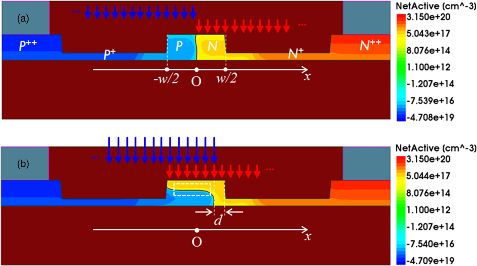
Figures 1(a) and 1(b) show the cross-sectional device structures of the Si LPN and LSPN optical phase shifters, respectively. The devices can be fabricated using conventionally available Si photonics foundry services. The Si waveguide width (w) is 450 nm designed for the C band. The mesa is 160 nm and the Si slab thickness is 60 nm. Si regions are p-type or n-type doped, and their doping levels are very heavy (p++-Si and n++- Si, ∼1020 cm−3) for ohmic contact, heavy (p+-Si and n+-Si, ∼1019 cm−3) for low series resistance, and light (p-Si and n-Si, ∼0.2 to ∼1.0 × 1018 cm−3 depending on dose conditions) for optical phase shift. As shown in the figures, NetActive shows free-carrier concentrations and the number of electrons (positive number) and holes (negative number), and PN junctions are clearly shown within the Si rib waveguides.

Fig. 1. (Color online) Cross-sectional carrier depletion-type optical phase shifters with (a) a lateral PN junction (LPN) and (b) an L-shaped PN junction (LSPN). NetActive indicates electron and hole concentrations for positive and negative numbers, respectively.
Download figure:
Standard image High-resolution imageTable I shows the ion implantation conditions for the LPN and LSPN junction formation. The LPN is formed by two implantation steps for each phosphorus and boron atom with two different implantation energies and the same dose amount. The implantation areas are from the center of the Si waveguide to n++-Si and p++-Si sides, respectively. The LSPN is formed by triple phosphorus implantation followed by double Boron implantation. The implantation areas are from the left-hand edge of the red arrows (–w/2) to the n++-Si side for phosphorus and from the right-hand side blue arrows (w/2–d) for boron. Here, d is the distance between the right-hand edge of the Si waveguide and the right-hand edge of the boron implantation region. Importantly, the dose amount for Boron is twice as large as that of phosphorus so that the doping type can be changed to p-type from n-type after boron implantation with a larger dose amount. In addition, it is noticeable that there is no significant cost issue in forming LSPN because only one more ion implantation step for boron is required and no additional masks are required compared to the LPN formation. The implantation energies are optimized to form the boundary of PN junction in the white dashed rectangle in Fig. 1(b) as horizontally as possible considering VpiL, phase shifter loss and cutoff frequency, and this greatly contributes optical phase shift. First, the three energies of phosphorus are chosen for peak densities to be uniformly positioned along the vertical direction in the rib waveguide, perpendicular to x-axis. Then, the two energies of boron with a twice as large dose are designed in such way to minimize the product of VpiL and loss but with a larger cutoff frequency than 30 GHz. Since the holes in Si are shown to be highly effective and have less loss, 8) a more efficient structure design would be arranging n-Si for the top and p-Si for the bottom than the opposite way. 19–21) Therefore, this would result in a lower VpiL and phase shifter loss. In detail, the common conditions are a 7-degree tilt angle with four 90-degree rotations and a 5 nm screening SiO2 layer on the top of Si waveguides for ion implantation. After the ion implantation process of other regions is completed, rapid thermal annealing for dopant activation is implemented at 1050 ℃ for 5 s.
Table I. Boron and phosphorus implantation conditions for LPN and LSPN optical phase shifters.
| Boron | Phosphorus | |||
|---|---|---|---|---|
| Dose (1 × 13 cm−2) | Energy(keV) | Dose (1 × 13 cm−2) | Energy (keV) | |
| LPN | n | 28 | n | 75 |
| n | 135 | |||
| n | 45 | n | 30 | |
| LSPN | 2n | 35 | n | 80 |
| 2n | 45 | n | 135 | |
3. Simulation result and discussion
To simulate the optical characteristics of modulators, Synopsys TCAD Sentaurus to calculate the carrier concentration and Lumerical optical mode solver for optical waveguides were used. The carrier concentration was calculated as a function of the applied DC reverse bias between the contact regions on the p++- and n++-Si. To simulate the optical characteristics, Soref's model for the changes in the refractive index and absorption coefficient in Si was used. 8,9) The changes in the effective refractive index and absorption coefficient in the modulators are extracted by using the optical mode solver with the model. Details on our simulation method, which has been well calibrated and verified, can be found in. 18,22,23) We implemented this simulation at the variable dose conditions of n = 0.5 to 1.6 with 0.1 steps in Table I. Figure 2 shows the electro-optical phase shifter performance of the LPN and LSPN optical phase shifters. Figure 2(a) shows VpiL as a function of the phase shifter loss at 0 V under all dose conditions. The passive loss of 1.5 dB cm−1 is added to the optical phase shifter loss since only free-carrier absorption is included in TCAD simulation. As the dose increases, the number of free carriers increase, and so the phase shifter loss increases and VpiL decreases. We chose two conditions among them that are almost the same as the phase shifter loss near 10.5 dB cm−1 for a reasonable comparison of their change in effective refractive index (Δneff) dependent on the bias voltage. This is because the change is highly dependent on the loss, and thus doping density. Figure 2(b) presents Δneff as a function of bias voltage at the loss near 10.5 dB cm−1. The second-order polynomial fitting results are also plotted and will be used for large-signal simulation later. Since the Δneff and optical phase shifter loss are in a tradeoff relationship, we compared them at the almost same loss. LSPN shows much higher Δneff due to a larger overlap between the optical mode and PN junction compared to LPN. This might lead to overestimation of device performance when VpiL is estimated using near 0 V, such as—0.5 to 0 V or 0 to 0.5 V because the slope of Δneff becomes lower as the reverse bias increases. Also, modulators practically operate at large-signal voltages, e.g. 2 Vpeak-to-peak. Therefore, VpiL in this study is based on the phase shift differences between 0 and 2 V of the large-signal voltages. It is expressed as follows:
where L is the phase shifter length, φ is the phase shifter, and λ is the wavelength.

Fig. 2. (Color online) Electro-optical phase shifter performance of LPN and LSPN optical phase shifters: (a) modulation efficiency (VpiL) as a function of phase shifter loss at 0 V, (b) change in effective refractive index as a function of bias voltage at the phase shifter loss near 10 dB cm−1.
Download figure:
Standard image High-resolution imageIt is shown that VpiL values for LSPN are much smaller than that for LPN in all dose conditions. In particular, VpiL for LSPN at 10.5 dB cm−1 is 0.89 Vcm while that of LPN at 10.5 dB cm−1 is 1.76 Vcm, indicating that modulation efficiency is nearly doubled by using LSPN at the same loss. In addition, the figure-of-merit for the modulator of the product of the phase shifter loss and VpiL (αVpiL) is ∼9.3 VdB and ∼18.5 VdB, respectively. It is reasonable to compare two devices at the same loss because αVpiL is lower for lightly doped cases, compared to highly doped cases, depending on the loss. 18)
Figure 3 shows the electrical characteristics of the LPN and LSPN optical phase shifters. The simulated series resistance (Rs) and junction capacitance (Cj) across cathode and anode electrodes as a function of the phase shifter loss are shown in Figs. 3(a) and 3(b), respectively. As the loss increases, the series resistance decreases but junction capacitance increases due to an increase in the free-carrier density. When the reverse bias voltage of −2 V is applied, the Cj of LSPN decreases much larger than that of LPN, leading to a much more efficient modulation efficiency. However, mainly due to the large Cj, the cutoff frequency (fcutoff) of LSPN is smaller than that of LPN, which is calculated by fcutoff = 1/(2πRs Cj). 13) As Cj decreases by applying a reverse bias voltage, fcutoff increases. For LSPN, this is smaller than that of LPN, but it is still larger than 30 GHz.
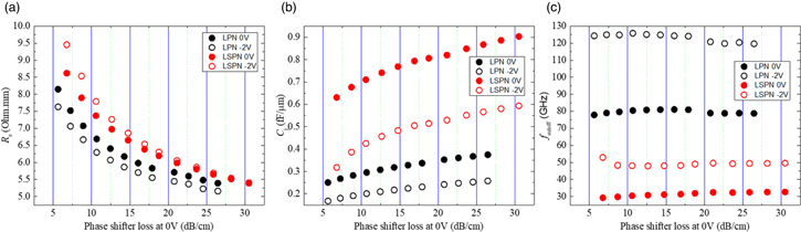
Fig. 3. (Color online) Electrical characteristics for LPN and LSPN optical phase shifters: (a) series resistance, (b) junction capacitance, and (c) cutoff frequency based on the intrinsic RC time constant of the active region.
Download figure:
Standard image High-resolution imageFigure 4 shows the d dependency on VpiL and fcutoff as a function of the phase shifter loss. Here, fcutoff at 0 V is only plotted because it is lower than that at −2 V due to the larger Cj, and the dynamic performance is limited by the lower fcutoff. For LSPN, it is possible to adjust VpiL and fcutoff because the Cj is adjusted by the design parameter, d. With an increase of d, VpiL decreases and fcutoff increases owing to the decrease in Cj. When d is 150 nm, the fcutoff is larger than 35 GHz, which enables the 50 Gbps NRZ data rate. 24,25)
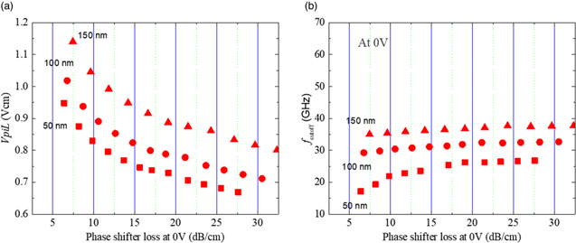
Fig. 4. (Color online) d dependency of (a) VpiL and (b) cutoff frequency as a function of phase shifter loss.
Download figure:
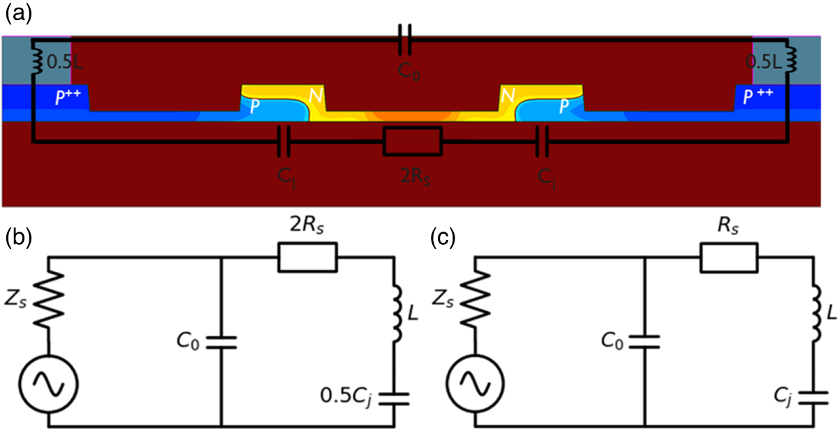
Standard image High-resolution imageSince the main drawback of LSPN is the smaller fcutoff due to the larger Cj compared to that of LPN, one could compensate by using a single-drive configuration, reported in, 26) shown in Fig. 5(a). Figures 5(b) and 5(c) show equivalent circuit models of single-drive (SD) and a half part of double-drive (DD) configurations for two phase shifters at both arms. Compared to the double-drive configuration, the two capacitances are connected in series for the single-drive configuration, so the Cj can be reduced by a half.
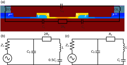
Fig. 5. (Color online) (a) Schematic of single-drive configuration and equivalent circuit models of (b) single-drive (SD) and (c) a half part of double-drive (DD) configurations.
Download figure:
Standard image High-resolution imageFor the quantitative analysis, we used the open-source electronic circuit simulator, Ngspice 27) for small- and large-signal responses. To verify our dynamic simulation methods, we first use this method to reproduce the reported results of S21 in the literature. 26,28) Experimental values from the literature 28) were used: C0 = 26 fF, L = 0.176 nH, Rs = 12.7 Ω and Cj = 0.26 pF. After the verification, we continue to use the values of C0 and L while Rs and Cj are given by our simulation for different structures and fabrication conditions. Although C0 and L are not as dominant as Rs and Cj, it is important to use reasonable and realistic value. Therefore, we used the experimentally reported values for C0 and L. Also, such a method was previously reported in the literature. 26) Our simulated 3 dB bandwidths of SD and DD are 11 and 19 GHz based on the SPICE, while the literature 28) shows 10.7 and 18 GHz, presenting a good agreement with our method.
Figure 6 shows the small-signal responses of S21 at 0 and −2 V for different input impedances. Both LPN and LSPN correspond to the devices in Fig. 1(a), in which the phase shifter losses are same. If a specially designed low Zs IC driver is used, this limitation can be eliminated 29,30) and RLC-limited performance will be dominant. 26) As expected, the LPN shows larger 3 dB bandwidths than LSPN. Since Cj is dominant for the S21, the 3 dB bandwidths increase when a reverse bias is applied and when SD is used instead of DD. In particular, the 3 dB bandwidth is improved by reducing Zs. As a result, the LSPN with a SD configuration shows a 3 dB bandwidth up to 26 GHz.

Fig. 6. (Color online) Small-signal response at 0 and −2 V for (a) and (b) Zs = 50 Ω, (c) and (d) Zs = 25 Ω, and (e) and (f) Zs = 10 Ω.
Download figure:
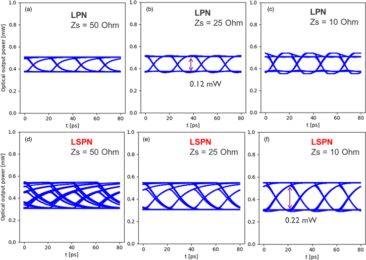
Standard image High-resolution imageIn addition, we implemented a large-signal simulation using the same two devices at the same loss, and the simulated 50 Gbps eye diagrams are shown in Fig. 7. The second-order polynomial-fitted functions of the bias-dependent Δneff, Rs, and Cj are used for large-signal modeling. The input optical power is assumed to be 1 mW and the input signal is PRBS 27 − 1 pattern with 4 Vpeak-to-peak without any pre-emphasis. For LPN, as predicted by the S21 results, the largest eye-opening is estimated to be 0.12 mW when Zs = 25 Ω. The speed is limited when Zs is too high (Zs = 50 Ω) and unnecessary peaking is seen when Zs is too low (Zs = 10 Ω). Regarding the time-domain peaking in Fig. 7(c), it corresponds to the frequency-domain peaking, fpeaking of S21 for LPN, SD, shown in Figs. 6(e) and 6(f). As Zs becomes smaller, the signal loss becomes smaller too. Thus, the peaking mainly caused by L and Cj appears near where it already exists in the range of 31 to 38 GHz (fpeaking ≃ 1/2π(LCj)0.5). For LSPN, both cases of Zs = 25 and 50 Ω show speed-limited eye diagrams, meaning total impedance is necessary to be reduced further. With a decrease in Zs, the eye diagram becomes much larger and the eye-opening is 0.22 mW (Zs = 10 Ω) which is 1.8 times larger than LPN. The eye diagram of LSPN might not be enough for error-free operation due to the limited EO response. However, it is possible for LSPN to use d to increase the EO response sacrificing modulation efficiency, as discussed in Fig. 4. Therefore, it will be important for the clearest eye diagram to optimize the LSPN design considering the tradeoff in a target optical link specification.
Fig. 7. (Color online) Simulated eye diagrams for 50 Gbps with a 27 − 1 pattern of SD configuration-based LPN for (a), (b), and (c) and LSPN for (d), (e), and (f) with different input impedances, Zs = 50 Ω, 25 Ω, and 10 Ω, respectively.
Download figure:
Standard image High-resolution image
4. Conclusion
A comparative study of Si optical phase shifters with lateral and L-shaped PN junctions was conducted by TCAD simulation. We show an easy-to-follow fabrication method for L-shaped PN junctions and the static device performance of both Si optical phase shifters. The L-shaped PN junction Si optical phase shifter shows much greater modulation efficiency of VpiL and lower optical phase shifter loss compared to the lateral one. Also, the large-signal simulation shows a dynamic optical modulation amplitude of 0.22 mW for the vertical one, which could offer a promising solution for a compact device footprint without a traveling wave electrode.
Acknowledgments
This work was supported by the research fund of Hanyang University (HY-2020-2750).