

Abstract
Compressed sensing (CS) has been proposed as a method of breaking the seemingly inherent tradeoff between sampling rate and resolution in a variety of applications, such as ultrasound imaging. Although various studies have demonstrated the effectiveness of using CS for sub-Nyquist sampling in ultrasound imaging, a dedicated integrated circuit (IC) has not yet been presented. This work introduces a single-chip mixer-based subarray beamformer, an important component for sub-Nyquist sampling in a CS ultrasound imaging system. The beamformer chip, which performs mixing, filtering, and summation of delayed signals within a subarray, is implemented using a single operational transconductance amplifier. We evaluated the performance of the proposed mixer-based subarray beamformer circuit fabricated using a 65 nm CMOS process with 0.4 mW ch−1 power consumption from a 1.2 V supply. Measurement results indicate that the prototype chip is suitable for subarray beamforming with a 5 ns resolution digital mixing sequence. The IC presented here is the first known implementation of a mixer-based subarray beamformer for sub-Nyquist sampling in ultrasonic applications and is expected to reduce sampling data requirements by a factor of 32.
Export citation and abstract BibTeX RIS

Content from this work may be used under the terms of the Creative Commons Attribution 4.0 license. Any further distribution of this work must maintain attribution to the author(s) and the title of the work, journal citation and DOI.
1. Introduction
Ultrasound imaging is an important and useful technique for point-of-care medical diagnosis, with many available commercial solutions. 1–3) Ultrasound imaging uses an array of transducer elements for tissue visualization. Conventionally, the lateral resolution of the array is dictated by the array aperture while the longitudinal resolution is dictated by pulse bandwidth (BW). In classical processing systems, the lower bound on the required sampling rate is related to the pulse BW. In particular, in portable applications as the number of channels increases with high sampling rate, it becomes more difficult to efficiently process the increased amount of sampled data from a transducer array with low power consumption. Therefore, a new processing paradigm is required to break this constraint.
Compressed sensing (CS) 4) techniques have attracted considerable research attention as a method to sample at the information rate of a signal. 5) In the CS technique, signals can be recovered from fewer measurements than that in the conventional Nyquist sampling technique 6) if the signal is sparse in some transform domains. CS technique has been proposed for applications in many areas, including in the fields of magnetic resonance imaging, 7) electroencephalogram, 8) and radar 9) to reduce the amount of measurement data. In particular, ultrasonic imaging devices that employ sub-Nyquist sampling are compatible with CS from the point-of-view of using pulses, 10) which can be shown as a finite rate of innovation model; 11) many studies have investigated the use of CS in sub-Nyquist sampling. 12–14) For example, a compressed beamforming technique that performs beamforming in the compressed domain was proposed. 15,16) Another study 17) developed an entire framework that exploits compressed beamforming and sub-Nyquist sampling, thereby enabling compressed ultrasound imaging using frequency-domain beamforming; their framework could reduce the sampling rate up to 28× compared with the standard beamforming sampling rate without substantially degrading imaging quality. Moreover, an advantage of employing a mixer-based subarray beamformer was reported using a printed circuit board assembly (PCBA)-based hardware implementation of an analog front-end. 18) However, to the best of our knowledge, there are no studies regarding the development of a single-chip mixer-based subarray beamformer with the exception of the international conference SSDM 2020 proceedings. 19) In this paper, building on the findings from previous proceedings, 19) we indicate more detailed chip measurement results and simulation results of the beamforming operation.
The rest of this paper is organized as follows. Section 2 describes the details of our designed system. In Sect. 3, we present the designed mixer-based subarray beamformer circuit. In Sect. 4, the measurement results of each functional block and system-level simulation results of our designed mixer-based subarray beamformer circuit are discussed. Finally, we conclude our work in Sect. 5.
2. System overview
2.1. Entire system
Figure 1 shows an example of the receiver part that has 64 transducers and consists of an 8-array mixer-based subarray beamformer. Imaging is performed by transmitting a beamformed pulse from an array of transducer elements. Propagation echoes are reflected by objects with an acoustic impedance mismatch (e.g. tissues), and the reflected signals are detected by the array elements. The received signals pass through a high-voltage switch used to switch between the transmit and receive paths, low-noise amplifier, variable gain amplifier, and mixer-based subarray beamformer. In the beamformer, each received signal is mixed to the baseband using a time-varying digital mixing sequence to effect phase delays and passed through a low-pass filter with a cut-off frequency that is considerably lower than the physical signal BW. This mixer-based subarray beamformer simultaneously applies both a frequency downconversion as well as an element-specific time-varying phase shift which acts as a narrowband time delay for that element. 18) This architecture assumes a complex mixer, generating both I and Q branches for sampling by the sub-Nyquist analog-to-digital converter (ADC). Subsequently, beamforming on the compressed signal and CS recovery are performed in the digital domain. In this study, NESTA 20) is used for the CS reconstruction algorithm.

Fig. 1. Entire system with mixer-based subarray beamformer and sub-Nyquist sampling ADC. Mixer-based subarray beamforming in the analog domain is used to reduce the sampling rate of the ADC.
Download figure:
Standard image High-resolution image2.2. Operation of mixer-based subarray beamformer
The dynamic range of the received signals can be increased by coherently summing the received signals. 21) This process is called beamforming and is one of the most important techniques in ultrasound imaging. Two common architectures for beamforming include single-stage beamforming and subarray beamforming. Single-stage beamforming architectures result in high data rates as each transducer requires a high-rate sampler. Therefore, if there are many transducers, single-stage beamforming is not suitable for low-power ultrasound imaging devices. The subarray beamforming technique, in which the array is divided into subarrays for applying delays to each subarray element and summing the delayed signals, is used to overcome the limitation of single-stage beamforming. 22) Subarray processing reduces the number of active array channels while maintaining image quality. Some previous works have demonstrated subarray beamforming in integrated circuits (ICs). 23–25) This work, aimed at a 64-element transducer array, implements subarray beamforming to process the received signal. The design choice of using eight receive elements per subarray was selected based on the system-level optimization presented in prior work. 26)
Figure 2 shows the block diagram of the mixer-based subarray beamformer. The block diagrams for the I- and Q-phase mixer-based subarray beamformer are the same; however, the digital mixing sequences I(t)[8K − 7]–I(t)[8K], Q(t)[8K − 7]–Q(t)[8K] for realizing the Kth subarray I- and Q-phase modulations are different. The input signals are modulated by digital mixing sequences to perform mixer-based beamforming; I- and Q-phase mixing signals in the digital mixing sequence bus are provided by a digital signal processor or a field-programmable gate array. The digital mixing sequences on the ith element I-phase I(t)[i] and Q-phase Q(t)[i] are equated as


where f0 and θ(t)[i] denote the center frequency of the reflected ultrasound and the time-varying phase term to implement the desired subarray beamforming delay, respectively. The modulated signals are then summed to realize beamforming as described in prior work. 26) The signal then passes through the filter and is band-limited for digitizing using a sub-Nyquist sampling ADC. In this work, a second-order Butterworth filter is chosen as a band-limited filter.

Fig. 2. Block diagram of designed mixer-based subarray beamformer [K].
Download figure:
Standard image High-resolution image2.3. System requirement of mixer-based subarray beamformer
Key system-level specifications for the subarray beamformer IC (such as dynamic range and BW) were determined through simulation. To guide our system-level specification design, a reference image was generated from the Field II ultrasound simulation program 27) was used. In this study, we selected images with high contrast and evaluated the images after reconstruction. The reference image and sub-Nyquist reconstructed image were compared using the structural similarity (SSIM) index. 28) Figure 3 shows the relationship between the SSIM index versus the dynamic range required for the circuits with various BWs. A combination of narrow BW, low dynamic range, and high SSIM index is required to achieve high image quality and low power dissipation. The required target SSIM varies depending on the application. We chose a design point of BW = 1.25 MHz and dynamic range of 65 dB to realize low power dissipation while maintaining reasonable performance with SSIM = 0.55.

Fig. 3. (Color online) Relationship between SSIM and dynamic range required for circuits with various BWs. We chose a design point of BW = 1.25 MHz and dynamic range of 65 dB to realize low power dissipation while maintaining reasonable performance with SSIM = 0.55.
Download figure:
Standard image High-resolution imageFigure 4 shows (a) reference image using a sampling rate of 20 MS s−1, and (b) CS-recovered result with 65 dB dynamic range and a sampling rate of 2.5 MS s−1. The time resolution of the digital mixing sequences used for frequency-domain beamforming was set to 5 ns. Although these images are similar; the sampled number of data can be reduced by a factor of 32. We see an 8× reduction in ADC sampling rate per mixer branch (from 20 to 2.5 MS s−1), but as each channel is complex, the low-rate sampler architecture results in a global savings of 4× in data rate. An additional factor of 8× in data rate savings is achieved by subarray beamforming of the 64 physical channels into 8 beamformed channels prior to sampling.

Fig. 4. Comparison of ultrasound image quality. (a) Reference image generated from the Field II ultrasound simulation program (sampling rate of 20 MS s−1). (b) CS-recovered result (65 dB dynamic range and sampling rate of 2.5 MS s–1).
Download figure:
Standard image High-resolution imageFor the system design, it is important to determine the necessary dynamic range for each block while considering the overall noise budget. We partitioned the noise contributions of each block as follows. We designed the framework for a 72 dB dynamic range for the subarray beamformer, 68 dB for the sub-Nyquist sampling ADC, and assumed 70 dB for other contributing circuits to achieve the 65 dB requirement as described above.
3. Design of mixer-based subarray beamformer
Figure 5 shows our designed circuit schematic of the low power mixer-based subarray beamformer. All eight inputs are input as differential signals; the digital mixing operation is achieved by inverting the sign of the signal at the mixing rate. This circuit is unique in that it uses only a single operational transconductance amplifier (OTA) to perform all functions of the mixer-based analog beamformer (mixer, adder, and second-order filter). This circuit configuration is based on the previously reported Gm-RC filter circuit configuration. 29) The transfer functions of the Kth mixer-based subarray beamformer are given as
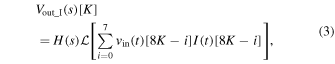


Fig. 5. Designed I-phase part mixer-based subarray beamformer [K] that uses only a single OTA to perform functions of mixer, adder, and second-order filter.
Download figure:
Standard image High-resolution imageHere, the transconductance of the input pair in the OTA is designed as  . Each parameter of the filter is hence


We design R1 = R2 = 24 kΩ, C1 = Cc = 33 pF to achieve a quality factor Q = 0.707; the cut-off frequency  is 1.25 MHz, and the required dynamic range is at least 72 dB. To consider process variation, C1 and Cc comprised capacitor banks with fourteen 3.3 pF unit capacitors.
In addition to gain and BW specifications, we also considered slew-rate requirements for this OTA. To minimize OTA power consumption, we limit the maximum input voltage to the circuit to be 100 mVpp. Figure 6 is designed as a two-stage conventional OTA for a mixer-based subarray beamformer; Rc is chosen as 220 Ω to eliminate zero of the designed OTA. The power supply voltage is 1.2 V.

Fig. 6. Two-stage OTA to be used for the mixer-based subarray beamformer.
Download figure:
Standard image High-resolution image4. Fabrication and evaluation results
4.1. Chip fabrication and evaluation board
A prototype chip was fabricated using the 65 nm CMOS process; Figure 7 shows a micrograph of the prototype of the mixer-based subarray beamformers (I- and Q-phase). The length of the I- or Q-phase mixer-based subarray beamformer block is 640 μm. The resistors R1 and R2 are arranged in the same block to minimize mismatch. The power dissipation is 1.6 mW per 8 channels in each circuit.

Fig. 7. (Color online) Micrograph of a fabricated chip in the 65 nm CMOS process.
Download figure:
Standard image High-resolution imageFigure 8 shows a photograph of the designed 6-layer PCBA used to evaluate our designed mixer-based subarray beamformer chip. This PCBA is equipped with single-to-differential and differential-to-single circuits that have sufficient performance to enable functional verification for such chips. Our prototype chips were encapsulated in a QFP package, which interfaced to the PCBA through a QFP socket. In addition, there are driver circuits for digital mixing sequence, input signal selector, and connectors around the PCBA to supply power for the respective circuits.

Fig. 8. (Color online) PCBA designed to measure prototype chip characteristics.
Download figure:
Standard image High-resolution imageIn the next subsection, we will first demonstrate performance of the mixer, adder, and filter blocks. We will then discuss the measured mixer-based delay performance, the key to subarray beamforming. After confirming that each function performs without any problems, we confirm the effectiveness of the proposed mixer-based subarray beamformer through system simulation with eight sub-arrays (64 channels).
4.2. Evaluation of filtering, summation, and mixing functions
Figure 9 shows the frequency response of the fabricated mixer-based subarray beamformer. Nine cutoff frequencies (modes) can be realized by the capacitor bank. By using mode 4, we can achieve the desired cut-off frequency as 1.25 MHz. From the measurement results, second-order filter characteristics are obtained as designed. Figure 10 illustrates the results of the analog summation with a 100 mVpp input; the signal strength increases when the signals are added while the frequency responses are not affected. Therefore, the measurement results show that the function of summation works as expected. Figure 11 shows the measurement result of mixing. The input signal is a 4.5 MHz sine wave, and the clock signal used as mixing sequence is 4 MHz. It can be seen that the frequency conversion has been achieved from the measurement result. These measurement results indicate that each function—filter, adder, and mixer—of the proposed mixer-based subarray beamformer performed as expected. Finally, the dynamic range of the fabricated beamformer circuit was confirmed by measuring the multi-channel integrated output noise. When measuring the noise, all input terminals of the fabricated beamformer circuit were connected to the half-VDD voltage. Figure 12 is a histogram of 15 prototype chip dynamic ranges. These results indicate that the design requirement of dynamic range of 72 dB was achieved.

Fig. 9. (Color online) Measured frequency response of the filter function in the mixer-based subarray beamformer. Second-order filter characteristics are obtained as designed. (a) Magnitude plot. (b) Phase plot.
Download figure:
Standard image High-resolution image
Fig. 10. (Color online) Measurement characteristics of the adder function in the mixer-based subarray beamformer when the number of input signal is changed. The signal strength increases when the signals are added while the frequency responses are not affected.
Download figure:
Standard image High-resolution image
Fig. 11. (Color online) Example measurement result showing the output of the mixer-based subarray beamforming block when using a 4 MHz clock signal and 4.5 MHz input signal. It is clear that the desired 0.5 MHz mixing product is achieved.
Download figure:
Standard image High-resolution image
Fig. 12. Histogram of dynamic range calculated by measuring the multi-channel integrated output noise of 15 chips. These results indicate that a dynamic range of 72 dB is satisfied, demonstrating successful achievement of the design requirement.
Download figure:
Standard image High-resolution image4.3. Evaluation of delay function
In this subsection, we evaluate the mixer-based delay operation, which is the core block behind the subarray beamforming operation. In the verification, the same sinusoidal input signal is applied to two beamformer circuits, and two types of clocks with different phases are used for each beamformer to set the digital mixing sequence. An NI PXIe-6545 waveform generator is used for clock generation, and a tunable clock delay is realized with a resolution of 5 ns. Figure 13 illustrates output waveforms of two beamformer circuits when input signal frequency is 4.5 MHz and frequency of the two clock signals is 4.55 MHz. The time difference between the clock signals is 5 ns. It is observed that two 50 kHz sine waves are realized with a phase shift after the mixing starts. The measured output signal time delay τd is around 455 ns. Figure 14 illustrates the relationship between the frequency of the input signal finput and the delay of the measurement output signal. The phase delay was detected by capturing the output signal with a 20 GS s−1 oscilloscope. BW limitation, averaging, and hysteresis judgment operation were employed to reduce the noise inside the oscilloscope enabling accurate measurement of the phase delays. In Fig. 14, equivalent time delay τeq is taken as the vertical axis to make it easier to understand whether the intended delay has been achieved. τeq can be calculated by using finput, clock frequency fclock, and τd as


Fig. 13. (Color online) The yellow curve shows the mixed product with no delay in the mixing signal, and the green curve shows the mixed product with 5 ns delay applied. It is clear that applying a per-channel delay to the mixing signal results in a time-shifted mixed product.
Download figure:
Standard image High-resolution image
Fig. 14. (Color online) The phase delays in the output signals when the input signal was changed were confirmed by measurement. Regardless of the frequency, equivalent time delays of 5 and 10 ns were achieved as expected.
Download figure:
Standard image High-resolution imageFrom Fig. 14, we observe that τeq remains the same, regardless of finput. Figure 15 shows τeq at finput = 3.3 MHz with varying clock delays. From the measurements, it is found that τeq increases with the delay. From the above measurement results, it is confirmed that the prototype chip can be used in a frequency-domain beamforming system that can realize a delay with a minimum time-shift of 5 ns.

Fig. 15. Measured equivalent time delay τeq for different clock delays of the mixer using finput = 3.3 MHz. It is observed that τeq increases linearly with clock delay.
Download figure:
Standard image High-resolution image4.4. System evaluation in simulation
We used a simulation to evaluate the performance of the proposed beamformer circuit operation in our system; in this evaluation, the 32nd path in the middle, where the largest signal level difference is realized, is used [Fig. 16(a)]. Figures 16(b) and 16(c) show simulated data passed through an ideal MATLAB mixer-based subarray beamformer model (blue) and transistor-level mixer-based subarray beamformer model via Spectre simulation (red). Figure 16(b) shows the I-phase results whereas Fig. 16(c) shows the Q-phase results. The horizontal axis represents the sample count, whereas the vertical axis shows the output signal obtained from the beamformer. It is evident that our designed transistor-level model simulation results are similar to those obtained by ideal mixer-based subarray beamforming in the system operation.

Fig. 16. (Color online) Behavior of the proposed mixer-based subarray beamformer was evaluated with Spectre simulation results and ideal results by MATLAB. (a) Evaluated image position. (b) I-phase results. (c) Q-phase results.
Download figure:
Standard image High-resolution image
4.5. Comparison
To the best of our knowledge, we have reported the first integrated mixer-based subarray beamforming IC for ultrasound imaging. We therefore compared the result of our designed beamformer with those of the recently reported time-domain beamformers 30,31) (Table I). The beamformer part of the previous study 30,31) consists of analog delays and adder circuits to perform beamforming on the time-domain signal. On the other hand, our mixer-based beamformer consists of a mixer, an adder, and a second-order filter for BW limitation. Comparing only the beamforming block, the power consumption of our mixer-based beamformer is lower than that presented in TBCAS2015 31) but slightly higher than that of the one presented in JSSC2019. 30) However, our proposed circuit has an advantage as an IC for the beamformer since it allows for fine-tuning down to 5 ns resolution digital mixing sequence.
Table I. Comparison of analog beamformers.
| This work | JSSC2019 30) | TBCAS2015 31) | |
|---|---|---|---|
| Technology | 65 nm CMOS | 180 nm CMOS | 130 nm CMOS |
| Beamforming domain | Frequency | Time | Time |
| Functions | Mixer, Adder, | Analog delay and Adder a) | Analog delay, Adder, |
| and Filter (2nd order) | and clock controller b) | ||
| Power dissipation | 0.4 mW ch−1 c) | 0.19 mW ch−1 a ) | 5.4 mW ch−1 b ) |
| (Only beamformer) | |||
| Delay time resolution | 5 ns d) | 25 ns | 4 ns |
a)Only BDR-SCD + CDADD. b)Only OTA + sampling/adding clock controller. c)Including I- and Q-both phases. d)Supported digital mixing sequence time resolution.
5. Conclusions
A single-chip mixer-based subarray beamformer used in a sub-Nyquist framework for ultrasound imaging with CS was proposed. In this work, we defined the specifications of the mixer-based subarray beamforming block through system-level simulations, using SSIM to measure reconstructed image performance. Next, we proposed a single-OTA architecture that met these requirements and simultaneously performed mixing, signal summation, and filtering for a subarray. Finally, we presented measured silicon results demonstrating that the subarray-based beamformer met the specifications previously laid out. The power consumption was 0.4 mW ch−1 from a 1.2 V supply. The measurement results indicate that the prototype chip can be used for frequency-domain beamforming with low power dissipation and a fine 5 ns time resolution digital mixing sequence. We evaluated the beamforming operation of the chip in simulations. The IC presented here is the first known implementation of a mixer-based subarray beamformer for sub-Nyquist sampling in ultrasonic applications and is expected to reduce sampling requirements by a factor of 32.
Acknowledgments
This research was partially supported by JSPS Overseas Research Fellowships and the Inamori Research Grant Program. Chip fabrication was provided by the TSMC University Shuttle Program.