
Abstract
With the fast-shrinking of the transistor dimensions, the low-frequency noise level considerably increases emerging as an important parameter for the design of advanced devices for information technologies. Single-trap phenomena (STP) is a promising approach for the low-frequency noise suppression technique in nanotransistor biosensors by considering trapping/detrapping noise as a signal. We show a noise reduction mechanism offered by STP in nanoscale devices making the analogy with stochastic resonance effect found in biological systems by considering a single trap as a bistable stochastically driven nonlinear system which transmits and amplifies the weak signals. The STP noise suppression effect is experimentally demonstrated for the fabricated liquid-gated nanosensors exploiting STP. We found the optimal conditions and parameters including optimized gate voltages to implement a stochastic switching effect for the extraction of useful signals from the background noise level. These results should be considered for the development of reliable and highly sensitive nanoscale biosensors.
Export citation and abstract BibTeX RIS
1. Introduction
The ultimate detection of the target analyte with the enhanced signal-to-noise ratio (SNR) and high sensitivity even at the single-molecule level is the priority task for modern bioelectronics. With the recent achievements and advancement in nanotechnology, liquid-gated (LG) nanowire (NW) field-effect transistors (FETs) have emerged as a basis for the development of reliable, high-speed, and highly sensitive biosensors capable of direct electrical detection and monitoring of the target analyte in a real-time manner and high sensitivity. 1–4) Although many promising biosensing results using NW FET-based biosensors have been recently achieved and reported in the literature, 5–8) the performance and sensing capabilities of such nanoscale biosensors are still limited by the electrical noise generated in the underlying transistor-based transducers at low frequencies. 5,9–11) Therefore, careful consideration and understanding of noise mechanisms in the aforementioned devices as well as investigation of possibilities to suppress the low-frequency noise in order to enhance the performance of NW FET biosensors are extremely important tasks.
Spontaneous fluctuations of the electrical signal (i.e. electrical noise) are inherent for any electrical device and typically have different sources and physical mechanisms. 9,12,13) Despite that, in NW FET biosensors, random trapping/detrapping of charge carriers usually dominates above other noise sources and defines a noise level of the transistor-based device at low frequencies. However, the number of electrically active traps considerably reduces as device dimensions shrink to the nanoscale. Subsequently, if the small-area transistor contains only a single active trap that randomly exchanges charge carriers with the conductive channel [see Fig. 1(a)], a discrete characteristic switching of the transistor drain current, i.e. random telegraph signal (RTS) noise appears as single-trap phenomena (STP). 9,14–16) Such an RTS effect is usually avoided as it increases the noise level of the nanoscale device. However, when RTS parameters (i.e. trap occupancy probability, RTS characteristic time constants) are monitored, then RTS becomes a signal of interest that contains useful information about the analyte interacting with nanotransistor device. 17,18) With this perspective and due to the strong dependence of RTS parameters on the surface potential change, STP in LG NW FET biosensors was recently proposed and demonstrated for the advanced biosensing with enhanced sensitivity. 18–20) Moreover, except for the sensitivity enhancement, STP in nanoscale devices offer a unique possibility for noise suppression due to the discrete nature of the effect. 21,22) The STP-based noise reduction mechanism is schematically demonstrated in Fig. 1(b). Unlike the classical transistor-based biosensors, where a shift of the threshold voltage is the signal and voltage fluctuations are the noise, the signal in such STP-based biosensors is a trap occupancy probability (i.e. g-factor) and fluctuations of this parameter are the noise. Therefore, the use of STP allows suppression of low-frequency noise in an approach that is similar to the stochastic resonance effect 23–27) taking into account that RTS is a stochastic switching process that can be considered as a white noise below a cut-off frequency. The idea beyond this is the discrete nature of RTS noise generated by a bistable stochastically driven single trap in a nanosensor device. Below a cut-off frequency, the RTS process can be considered as white noise which is added to the signal of interest, i.e. the change of the surface potential as a function of target biomolecules. 18) Therefore, by monitoring RTS parameters, the signal can be detected with enhanced SNR. In this regard, the novel detection approach based on STP obviously has some similarities with the SR effect which allows amplifying the weak input signals with the help of system white noise. As a result, the low-frequency noise can be suppressed by monitoring the g-factor as a signal even below the dielectric-polarization noise 5,28) level defining the thermal limit for the state-of-the-art NW FET-based biosensors. For this challenge, the variation of g-factor parameters as a function of the gate voltage applied remains unexplored.
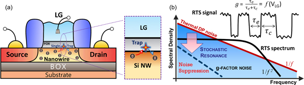
Fig. 1. (Color online) (a) Schematic illustration of STP in a liquid-gated NW FET biosensor. (b) The noise suppression approach due to STP in the regime of stochastic switching. The use of RTS noise that appears due to STP as a signal allows noise suppression upon understanding and careful selection of optimized conditions. All drawings are shown schematically.
Download figure:
Standard image High-resolution imageIn this paper, we investigate the gate-voltage dependence of the g-factor noise and reveal the noise suppression effect due to STP in nanoscale devices. For this purpose, silicon NW structures configured as LG accumulation-mode p-type FETs were fabricated and studied from the perspective of STP performance and g-factor noise. Three STP-related parameters: time window, RTS corner frequency (i.e. trap operation frequency), and a slope of g-factor dependence as a function of the gate voltage applied are considered. The experimental data prove and demonstrate that low-frequency noise in the nanoscale devices can be suppressed by orders of magnitude for devices exploiting STP.
2. Experimental methods
2.1. Fabrication of LG Si NW FETs
LG Si NW FET biosensors were fabricated using silicon-on-insulator (SOI) wafers with 50 nm thin 〈100〉-oriented Si layer and 145 nm thick buried oxide layer. SOI wafers were commercially purchased from SOITEC, France. Widths of designed and fabricated NWs are in the range from 70 to 500 nm and lengths vary in the range from 100 nm to 4 μm. The detailed steps involved in the fabrication process of Si NW structures were previously reported and can be found elsewhere. 2,29) Briefly, before NW patterning, SOI wafers were covered with a 20 nm thick SiO2 layer using PECVD to serve as a layer for hard mask formation employing reactive ion etching. The NW pattern was defined using e-beam lithography and mesa structures were defined utilizing photolithography. After this, structures were transferred into the active silicon layer of SOI wafers using wet chemical etching in tetramethylammonium hydroxide (TMAH) solution. Afterward, ion implantation was performed with Boron dopants to create accumulation mode FETs (p+–p–p+) transistor structures. Then, an 8 nm thin SiO2 layer was thermally grown on the NWs to serve as the gate dielectric and protect the conductive channel of transistor-based biosensors from the liquid environment. The metallization process was then performed by sputtering of a metal stack consisting of 5 nm TiN and 200 nm of Al followed by the lift-off patterning and annealing process. To protect metal leads against the liquid environment, the structures were passivated with a polyimide layer. The access of the liquid solution to Si NWs was provided by patterning the passivation layer with photolithography. After the fabrication process wafers were cut into chips which were further wire-bonded, encapsulated with polydimethylsiloxane (PDMS), and used for the experiments. All the fabrication steps were performed at the Helmholz Nano Facility of Forschungszentrum Jülich.
2.2. Electrical noise characterization
Noise characterization of the fabricated NW devices was performed using a modernized and fully automated ultralow-noise measurement setup developed in-house. A detailed description of the setup can be found in Ref. 29. Briefly, the gate-source and drain-source biases are applied to the device-under-test (DUT) using a battery-operated and fully automated voltage supply system which allows precise electrical biasing of DUT with the accuracy approaching 1 mV. The Agilent U2542A simultaneous data acquisition analog input channels in polling mode configuration are used to control and measure all the voltages applied. However, the Agilent voltmeters are disconnected from the noise measurement circuit during the noise data acquisition to avoid any impact on noise measurement results. The noise measurements are performed using an analog input channel in the AC configuration. First, the signal (time-dependent source-drain voltage fluctuations) is preamplified using an ultralow-noise homemade pre-amplifier with a gain of 172. Then, the signal is passed through the commercial amplifier ITHACO 1201 with a variable gain from 1 to 10k and further amplified with a low-noise general-purpose programmable-gain amplifier PGA-103. Note, to exclude the influence of the amplification cascade the measurement system has been calibrated before noise measurements. At maximum amplification, the noise level of the noise measurement setup is low as  at 10 Hz. Afterward, the signal is filtered using digitally controlled antialiasing continuous-time filter LTC 1564. Finally, the measured time-dependent source-drain voltage fluctuations are transferred to a PC via a high-speed USB 3.0 interface were then translated into a voltage power spectral density. As a result, the noise measurement setup allows acquiring the noise spectra in the frequency range from 1 Hz to 100 kHz and time-traces of the voltage fluctuations with the sampling rate up to 500 kHz. To obtain reliable noise characteristics of DUT, noise measurements are performed inside a metal Faraday cage to shield against external electromagnetic radiation and other parasitic disturbances.
2.3. Evaluation of g-factor noise from RTS voltage fluctuations
To evaluate the g-factor noise from the RTS time trace, we proposed and employed a so-called sliding window algorithm that is schematically demonstrated in Fig. 2. More precisely, we extract g-factor g(t) over a given time window Θ directly from the time distribution of RTS voltage fluctuations. Then, by sliding the window along with the RTS time trace, a new time trace with the trap occupancy factor fluctuations in time is constructed. Finally, the time-domain data of g-factor noise can be then translated into a frequency spectrum resulting in the power spectral density 
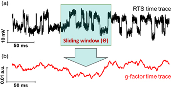
Fig. 2. (Color online) Schematic representation of the conversion of (a) RTS voltage fluctuations into (b) the time-dependent fluctuations of g-factor.
Download figure:
Standard image High-resolution image3. Results and discussion
3.1. RTS noise in fabricated Si NW FETs
In this study, we focus on the noise suppression effect offered by STP in nanoscale devices. Therefore, only NW FETs demonstrating RTS noise are of interest. Figures 3(a)–3(d) show typical RTS time traces as time-dependent fluctuations in the drain current measured on 100 nm wide and 200 nm long Si NW FET that was operated at a constant drain-source bias of −20 mV and different liquid-gate voltages. The RTS measurements were performed in a physiological phosphate-buffered-saline (PBS) solution with 10 mM concentration and pH = 7.4 at room temperature. The liquid-gate potential was applied using Ag/AgCl reference electrode. The data clearly demonstrate that STP is well-pronounced in the tested device and dominates over all the other noise sources when a single trap is electrically active near the conductive channel of the NW FET. As a result of STP, the drain current of the nanostructure fluctuates between two distinct levels that correspond to the "capture" and "emission" states of the single trap. Clear two-state switching kinetic due to STP can be further evident from the corresponding amplitude histograms that are also shown in Figs. 3(a)–3(d). An analysis method based on a hidden Markov model 30,31) was then applied to extract the single-trap states for measured RTS time traces.

Fig. 3. (Color online) (a)–(d) Typical RTS time traces measured for the 100 nm wide and 200 nm long Si NW FET operated at constant  and different liquid-gate voltages, listed in the corresponding figures.
Download figure:
Standard image High-resolution imageThe mean duration of stay of a charge carrier in the capture and the following emission states are usually characterized by the average emission ( ) and capture (
 ) time constants, respectively. The corresponding average capture and emission time constants characterizing the registered RTS process are shown in Fig. 4(a) as a function of the liquid-gate voltage applied. As can be seen in Fig. 4(a), the average
  remains about constant in the range of the liquid-gate voltage applied, while the average
  displays a superlinear dependence on
  in the semilogarithmic scale suggesting a strong dependence of the RTS capture dynamic on surface potential controlled by the liquid gate. It should be noted that such behavior of RTS characteristic time constants is typical for LG NW FETs.
18,20)
in the semilogarithmic scale suggesting a strong dependence of the RTS capture dynamic on surface potential controlled by the liquid gate. It should be noted that such behavior of RTS characteristic time constants is typical for LG NW FETs.
18,20)

Fig. 4. (Color online) (a) Measured RTS characteristic capture and emission time constants plotted as a function of the liquid-gate voltage applied. The behavior of RTS time constants for LG NW FETs demonstrates that the capture time constant depends strongly on the liquid-gate voltage. The dashed colored lines represent a visual guide. (b) Liquid-gate voltage dependencies of the input-referred voltage noise (left axis) taken at 10 Hz and trap occupancy probability (right axis) for the measured RTS noise. The noise as a signal is maximized when 
Download figure:
Standard image High-resolution imageFigure 4(b) displays the liquid-gate voltage dependence of trap occupancy probability, g, calculated as

where  is the average emission time of a charge carrier from the trap and
  is the average time for a random charge carrier to be captured by the trap.
For STP in LG NW FETs, the gate-voltage dependence of g can be explained by a widened Fermi-type distribution due to the partial potential drop at the trap depth. Figure 4(b) shows that at low liquid-gate voltages, the probability of a charge carrier to be captured by the trap is small, while the latter is fully occupied at high  At
At  which corresponds to the case when the trap energy level coincides with the Fermi level of the system, the probability of the trap to be occupied is equal to 50% and therefore, the number of switching events between capture and emission states within the measured period of time is maximized. As a result, the RTS noise is also maximized when
  as can be evident in Fig. 4(b). However, below we show that if g is monitored as a signal, RTS noise becomes an object of increasing interest providing an excellent opportunity for noise suppression in an approach similar to the stochastic resonance.
3.2. STP to extract the signal from the background noise
Figure 5 shows the noise spectra of g-factor fluctuations calculated from the RTS voltage fluctuations at different liquid-gate voltages using the above-described sliding window approach. The g-factor time traces and corresponding g-factor noise spectra were obtained for the time window of  in this case. Figure 6(a) shows the gate voltage dependence of the evaluated g-factor noise,
  that was taken at the frequency of 10 Hz. As can be seen from Fig. 6(a), the maximum of the g-factor noise was observed at
  which corresponds to the case when
  At this condition, the number of trapping/detrapping events is maximized within a given time window resulting in the maximum of g-factor noise when calculating the trap occupancy probability. It should be emphasized that calculated
  noise as a function of liquid-gate voltage follows the gate voltage dependence of the g-factor slope squared [Fig. 6(a)]. The fact additionally supports the selection of optimal gate voltage at −0.8 V to utilize the full potential of STP for noise suppression.

Fig. 5. (Color online) Noise spectra of g-factor fluctuations calculated for the time window  and different liquid-gate voltages applied.
Download figure:
Standard image High-resolution image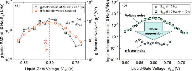
Fig. 6. (Color online) (a) Liquid-gate voltage dependencies of  noise at 10 Hz (left axis) and g-factor derivative squared (right axis). (b) The equivalent input-referred g-factor noise at 10 Hz as a function of
  calculated for the time window size of 10 s. The gate-voltage dependence of the input-referred voltage noise is derived from Fig. 3(a) and shown for the comparison. The arrow indicates the noise suppression from measured RTS voltage noise to calculated g-factor noise for the single trap in the regime of stochastic switching. Note, the lower
  noise compared to the voltage noise level was obtained for the entire range of the applied liquid-gate voltages due to electrically active single trap generating pronounced two-level RTS signal.
Download figure:
Standard image High-resolution image
To compare the noise caused by the current fluctuations in the channel and fluctuations of the trap occupancy factor, we calculate an equivalent input-referred g-factor noise,  similarly as for the input-referred voltage noise:

where  is the g-factor PSD and
  is the g-factor derivative calculated as
  The input-referred g-factor noise at 10 Hz calculated using Eq. (2) is shown in Fig. 6(b) as a function of the liquid-gate voltage. For the comparison, Fig. 6(b) displays also the input-referred voltage noise that was measured for the tested 100 nm wide and 200 nm long LG Si NW FET demonstrating pronounced two-level RTS noise. As can be seen in Fig. 6(b), the
  noise calculated for the time window
  is considerably lower than the measured voltage noise. This reveals that
  is a large enough time window for the meaningful statistical evaluation of the g-factor. Thus, these results clearly demonstrate that by monitoring the g-factor as a signal, the low-frequency noise in the nanosensors exploiting STP can, in fact, be suppressed by the selection of optimized conditions. Remarkably, the lower
  noise compared to the voltage noise level was obtained for the entire range of the applied liquid-gate voltages [Fig. 6(b)] due to electrically active single trap generating pronounced two-level RTS signal. The latter is an important parameter to improve sensitivity and SNR in NW FET biosensors.
4. Conclusions
STP in nano FET sensors offer an outstanding opportunity for the suppression of the low-frequency noise in an approach analog to the stochastic resonance effect found in biological systems. In contrast to the usual NW FET-based biosensors for which a shift of threshold voltage is a signal and voltage fluctuations are the noise, the signal for STP-based devices is trap occupancy probability and the fluctuations of this parameter become the noise. We systematically studied the gate voltage dependence of the g-factor noise parameters in LG NW FET structures. The results demonstrate that the low-frequency noise in the nanoscale devices can be suppressed by orders of magnitude for the devices exploiting STP. The exchanging processes between the single trap and carriers of the conductive channel should be considered as a unique solution of a challenge to increase the SNR in nanotransistor biosensors.
Acknowledgments
The authors acknowledge the Seed Money funds for supporting a new international collaboration as part of the RTS-Biosensor project. The authors also thank all the technical staff of the Helmholtz Nano Facility (HNF) of Forschungszentrum Jülich for their assistance with the fabrication of the sensors devices. This work was partially supported by the JSPS Core-to-Core Program (A. Advanced Research Networks). Y. Kutovyi greatly appreciates a research grant from the German Academic Exchange Service (DAAD). I. Madrid is grateful to the interdisciplinary research funds from CNRS for the BIOSTAT project.