

Abstract
In this study, a VO2 thin film was directly deposited on a soda-lime glass by reactive RF sputtering to investigate its potential application in smart windows. The VO2 crystal structure is susceptible to changes in the oxygen density; to decrease this sensitivity, we fabricated a VO2 thin film by increasing the RF sputtering power, rather than increasing the growth temperature. The orientation of VO2 was changed from (011) to (100) by increasing the RF power from 100 to 180 W. This phenomenon can be explained using the enthalpy compensation and strain effect. The thin film clearly shows thermochromic characteristics in terms of drastic variation in infrared radiation at different temperatures based on the intrinsic transition property of VO2. Direct deposition of VO2 thin film on a glass substrate using the high RF power sputtering method proposed in this study is recommended as a simple and low-cost method to add a self-temperature control function to smart windows.
Export citation and abstract BibTeX RIS
1. Introduction
Heat load management such as central control of heating and air conditioning in a building infrastructure is predicted to reduce approximately 30% of greenhouse gas emissions. 1,2) This data has encouraged research on methods to save energy to maintain a comfortable indoor environment for a central system in buildings. One approach for heat management is to develop a functional material coating in which the thermochromic function is activated through temperature control of infrared (IR) radiation on glass windows in a building.
Thermochromic materials such as NbO2, VO2, and TiO2 can be transformed from a semiconductor to a conductor and vice versa by controlling their temperature. 3) Of these, many researchers have focused on VO2 because its electrical conductance varies by several orders of magnitude at 68 °C from a semiconductor (with a high IR transmittance) to a metallic-like conductor (with a high IR reflectance). 4) In our research group, a visible-light transparent solar cell and a sensor have been developed for a smart window with several functions for the Internet of Things. 5,6) To add other functions to the smart window, we investigated VO2 as a self-temperature control element by blocking IR radiation at high temperatures (over 68 °C). Furthermore, fabricating a large area of a VO2 thin film on a glass substrate using a low-cost method and at an acceptable process, the temperature is necessary to realize a smart window for cost-effective optical applications.
Although several methods, such as chemical vapor deposition, 7) pulsed laser deposition, 8) metal-organic chemical vapor deposition, 9) physical vapor deposition, 10) and hydrothermal approach, 11) have been reported for VO2 deposition, these methods have limitations such as the need for a small area and a high temperature of over 600 °C in fabricating a well-defined VO2 film. To overcome these limitations, we used the sputtering method in this study, which can be employed to deposit a film on a large area using a relatively low temperature applied to the glass substrate. Zhao et al. conducted an experiment to achieve VO2 deposition using sputtering at a deposition temperature in the range of 550 °C–700 °C. 12) As the temperature increased, the ion state of V changed from V5+ → V4+ → V3+. A seed layer of ZnO, 13) TiO2, 14,15) Si, 16) muscovite, 17) and SnO2 18) is typically used to enhance the crystal quality and decrease the process temperature. However, in this work, adding a seed layer would have complicated the sputtering process and increased the fabrication cost. To achieve direct deposition of a VO2 film on a glass substrate at an appropriate temperature, we investigated the dependence and variation of RF sputtering conditions while directly growing a VO2 thin film on a soda-lime glass (SLG) substrate.
2. Experimental methods
A 50 nm thick VO2 thin film was deposited on cleaned SLG by RF sputtering. The SLG substrate was cleaned using acetone, followed by isopropyl alcohol in an ultrasonic cleaner for 30 min, respectively. During RF sputtering, the process temperature was fixed at 400 °C because the substrate is SLG, which has a strain temperature of approximately 500 °C. In reactive sputtering, the ambient directly affects the composition of the film, as reported in certain studies where VO2 was deposited in an H2 atmosphere to reduce oxygen from a V2O5 target. 19) However, in the present experiment, a VO2 target was used. We used a 4 in VO2 target with a purity of 99.99% and the distance between the target and the substrate was 60 mm. During sputtering, oxygen from the VO2 target easily turned volatile owing to the plasma; hence, forming VO2 was difficult. Therefore, an Ar-based mixture of O2 (5%) gas at a pressure of 2–3 Pa was used.
To characterize the crystallinity of the VO2 thin film, we collected X-ray diffraction (XRD) data of the samples using a Rigaku Ultima IV X-ray diffractometer operated at 40 kV and 40 mA with Cu Kα radiation. The sample's XRD patterns were measured with a step size of 0.01° and a counting time of 4 s. X-ray photoelectron spectroscopy (XPS) measurement was performed using a JPS-9000MC (JEOL Ltd.) with a step size of 0.5 eV. To measure the depth profile, we etched the film with energy from an Ar ion beam of 300 eV using an XPS measurement system. The transmittance characteristics were measured using a UV–vis spectrophotometer (V-670, JASCO). The homemade heating system for VO2 thin film deposited on the SLG glass was built in the V-670.
3. Results and discussion
The crystallinity and orientation of VO2 are strongly influenced by the surface state of the substrate, including the seed layer (ZnO, 20) TiO2, 21) SrTiO3, 22) and MgO 23)) and distortion. 24) In this experiment, ZnO and Al2O3 (c-sapphire substrate) were used as the seed layer to control the orientation and obtain better crystallinity of VO2. A 50 nm thick ZnO seed layer was deposited on the glass by sputtering with an RF power of 100 W in Ar/O2 (95/5) ambient. The sputtering method produced effects such as plasma damage on the substrate owing to the plasma. In this study, a relatively high RF power (180 W) was used; hence, the influence of RF power should be investigated first.
The representative XRD patterns of the VO2 thin films deposited on different seed layers using an RF power of 180 W in Ar/O2 (95/5) ambience are shown in Fig. 1. Diffraction peaks related to VO2(100) and (200) orientations are shown on the amorphous glass substrate. In the case of an amorphous substrate, two types of patterns have been reported for VO2(100) and (011), 10,18) which will be discussed in the next section. The VO2(020) peak at 39.9° appeared on the sapphire substrate as previously known, indicating that the orientation of VO2 can be controlled and grown as described in a previous report 8) even though the substrate is in a high plasma density. However, although a VO2 thin film deposited on ZnO usually shows VO2(020) orientation at 39.9° as reported in a previous study, 13) a small peak related to the mixture of V2O5 and VO2(002) can be observed on the 50 nm ZnO thin film in Fig. 1. The Zn atom can be easily diffused using a high substrate temperature and plasma energy; 25) consequently, VO2 is not formed on the ZnO thin film according to the XPS results, contrary to the diffusion and oxidation states of V in VO2 thin films deposited on Al2O3 and ZnO.
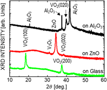
Fig. 1. (Color online) XRD patterns of VO2 films deposited on sapphire, ZnO, and glass substrates.
Download figure:
Standard image High-resolution imageFigure 2 shows the XPS spectra of the VO2 thin film deposited on ZnO and sapphire after etching for 5 s and 30 s, respectively. The main peak of O 1 s for both films is at 531.1 eV; further, there is a V-OH contaminated peak at the VO2 film surface (5 s etching) in Figs. 2(a) and 2(d) for VO2 deposited on Al2O3 and ZnO, respectively. As shown in Fig. 2(f), the intensity of Zn 2p is detected even at the surface (after etching for 5 s). The calculated Zn atom ratios at the surface of VO2 (5 s etching) and inside (30 s etching) VO2 were 1.2% and 7.5%, respectively. The diffused Zn atoms interfere with the bond between vanadium and oxygen because Zn–O (<250 kJ mol−1) has a lower enthalpy than V–O (637 kJ mol−1). 26) Thus, the V5+ ion is preferred owing to the oxygen deficiency of vanadium, as shown in Fig. 2(e). In contrast, for the Al2O3 substrate, Al atoms do not diffuse into the VO2 film, as shown in Fig. 2(c), and the film has more V4+ ions than V5+ ions, as shown in Fig. 2(b). Therefore, a seed layer that does not have an atom that can interfere with the composition of VO2 should be selected.

Fig. 2. (Color online) XPS spectra of (a) O1s, (b) V2p, and (c) Al2p for VO2 films deposited on Al2O3, and (d) O1s, (e) V2p, and (f) Zn2p for VO2 films deposited on ZnO.
Download figure:
Standard image High-resolution imageIn fact, V is a transition metal that is difficult to synthesize as it exists in several oxidation states obtained by forming various binary oxides. 27) Of these oxidation states, VO2(V4+) has a very narrow range in the V–O phase diagram; thus, VO2 is sensitive to variations in the oxygen ratio. 28) A higher process temperature provides a wider acceptable O2 density ratio range; 29) hence, previous works maintained a substrate temperature of over 500 °C. 15,17,24) Moreover, the oxidation state of V varied from 5+ to 3+ as the temperature increased from 550 °C to 700 °C. 12) In this experiment, the process temperature was fixed at 400 °C because the strain point (specific value at which the volume abruptly increases) of the SLG substrate is 490 °C. Therefore, the RF power was increased up to 180 W rather than increasing the substrate temperature to mitigate the sensitivity of oxygen.
Figure 3 shows the XRD patterns of the VO2 thin film deposited on the SLG substrate at an applied temperature of 400 °C with different RF powers of 100, 150, and 180 W in Ar/O2(95/5%). A small peak of VO2(011) at 27.8° occurred at an RF power of 100 W. This agrees with the result presented in Ref. 30, and these samples show susceptibility to oxygen density. Interestingly, a VO2 crystal orientation transition based on RF power is demonstrated for the first time. As the RF power increased, the orientation of VO2 shifted from (011) to (100), which has a higher peak intensity. At an RF power of 150 W, the film shows the coexistence of the peak of VO2(100) at 18.2° and the other intermediate compound (V2O5 and VOx
). It shows well-defined VO2(100) and VO2(200) orientations at an RF power of 180 W. The oxidation process in plasma with oxygen is complex because of many excited metastable states of oxygen molecules;
31) this requires further investigation in future works. In this analysis, two expectations are considered. First, a high plasma density can compensate for reaction energy because the enthalpies of vanadium oxides
32) are ∆
 = −1557 cal mol−1 and ∆
 = −713 cal mol−1, which facilitates the formation of V2O5 rather than VO2. A high plasma density provides the energy required to compensate for the difference in the enthalpy, similar to the effect of high temperature. Second, the strain state on the substrate changes because of high plasma density. The same pattern of changes in the crystal orientation reported in this work was also reported by Jung et al.
33) In the work by Jung et al., the trend of VO2 orientation was investigated on different (a-, c-, m- and r-) plane sapphire substrates where it was reported that the out-of-plane direction of VO2 occurred under compressive strain, whereas the in-plane VO2 orientation occurred under tensile strain. Under high plasma density, an ion cloud with high kinetic energy could be formed to induce compressive strain on VO2 film at low temperatures, producing an out-of-plane VO2(100) orientation.
34)
= −713 cal mol−1, which facilitates the formation of V2O5 rather than VO2. A high plasma density provides the energy required to compensate for the difference in the enthalpy, similar to the effect of high temperature. Second, the strain state on the substrate changes because of high plasma density. The same pattern of changes in the crystal orientation reported in this work was also reported by Jung et al.
33) In the work by Jung et al., the trend of VO2 orientation was investigated on different (a-, c-, m- and r-) plane sapphire substrates where it was reported that the out-of-plane direction of VO2 occurred under compressive strain, whereas the in-plane VO2 orientation occurred under tensile strain. Under high plasma density, an ion cloud with high kinetic energy could be formed to induce compressive strain on VO2 film at low temperatures, producing an out-of-plane VO2(100) orientation.
34)

Fig. 3. (Color online) XRD patterns of VO2 films at different RF sputtering powers.
Download figure:
Standard image High-resolution imageThe insulator–metal transition (IMT) temperature should be considered to practically utilize a smart window. The resistivities of the VO2 thin film during heating and cooling were measured at temperatures ranging from 30 °C to 125 °C, as shown in Fig. 4(a). The VO2 film exhibits clear IMT characteristics with two orders of resistance variation. The degree of resistance variation is relatively smaller than that observed in other studies 20,23) because of the relatively thin (50 nm) VO2(100) film. 20) The IMT temperature was obtained from the plot of dln R/dT versus T, as shown in Fig. 4(b). The IMT temperature is 72.5 °C, which was calculated as follows: (Tc + Th)/2 (Tc: cooling branch, Th: heating branch). This result is slightly higher than the ideal IMT temperature of VO2 (68 °C). The VO2(100) film also showed an IMT temperature of 68 °C. 7) Hence, the increase in the IMT temperature was expected owing to the inhomogeneities of the VO2 thin film, such as polycrystalline and Si impurity. 35)

Fig. 4. (Color online) (a) Resistivities and (b) dln(R)/d T curves of the VO2(100) thin-film as functions of measurement temperature.
Download figure:
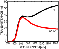
Standard image High-resolution imageTo evaluate the thermochromic property of the VO2 thin film for a smart window, we measured change in the transmittance. For smart window applications, the VO2 film should always allow visible light and block IR radiation at high temperatures. The temperature-dependent transmittance of the VO2 thin film deposited at a high RF power was measured at 25 °C and 80 °C, to estimate the modulation of transmission by the VO2 thin film, as shown in Fig. 5. In this experiment, to test the IR transmittance modulation, the temperature was set as 80 °C because the maximum temperature of glass was assumed to be approximately 80 °C, as specified by Agrawal; 36) the set temperature is higher than the IMT temperature of the VO2(100) thin film, obtained from Fig. 4(b). Thermochromic characteristics are clearly observed with drastic variations in the IR radiation at different temperatures. The VO2(100) thin-film modulates the transmittance to a 35% drop at 80 °C. To quantitatively evaluate the IR modulation function, 37) we formulated the integral transmittance of IR as follows:
where  is the solar irradiance spectrum for an air mass of 1.5 corresponding to the Sun being positioned 37° above the horizon and λ ranges from 780 to 1700 nm for an IR function. The calculated difference in
  at high temperatures and at room temperature is 17.6%. This integral IR transmittance modulation behavior was applicable to a smart window.
Fig. 5. (Color online) Transmittance spectra of the VO2 thin film at RT and 80 °C.
Download figure:
Standard image High-resolution image
Considerable work is still required to realize self-temperature control films capable of sensing temperature. This study investigated only the possibility of realizing such a device. These results of this study can serve as the first step toward realizing smart windows/greenhouse using high power density RF sputtered VO2 thin films.
4. Conclusions
In this study, a VO2 thin film was directly deposited on an SLG substrate by RF sputtering for a cost-effective optical implementation of self-temperature control, in which the RF sputter power was exclusively controlled. The study revealed that the crystalline of VO2 was changed from VO2(011) to VO2(100) by RF power increasing. The obtained VO2(100) at high RF power showed well-defined IMT property and IR transmittance modulation which are applicable for a smart window. Although further investigation is required to elucidate mechanisms such as the role of RF power and to enhance optical performance, the deposition of VO2 thin film by sputtering using high RF power shows sufficient potential as a simple and low-cost method of creating smart windows.