
Abstract
This research investigates the cause of lifetime reduction properties of a crystalline defect layer introduced by the plasma process such as reactive plasma deposition (RPD). The plasma irradiation damage to silicon substrate with the different oxygen and carbon concentrations were evaluated. Minority carrier lifetime of the silicon substrate after the RPD process has been significantly reduced by plasma irradiation. Furthermore, photoluminescence (PL) spectroscopy revealed that the cause of the lifetime degradation on the silicon substrate is Ci–Oi defect generation originated in the plasma irradiation during the RPD process.
Export citation and abstract BibTeX RIS

Content from this work may be used under the terms of the Creative Commons Attribution 4.0 license. Any further distribution of this work must maintain attribution to the author(s) and the title of the work, journal citation and DOI.
1. Introduction
Crystalline silicon solar cells are dominating the solar cells industry due to high efficiency with suppressed fabrication cost.1–3) For example, silicon heterojunction (SHJ) solar cell shows the high voltage and the high conversion efficiency over 25% by adopting the amorphous Si (a-Si) and crystalline silicon heterojunction.4–8) However, these still have a problem of reducing minority carrier lifetime by various crystal defects, such as impurities, precipitates and dislocations, which are inevitably introduced in the fabrication process.9–12) In order to reach the theoretical limitation of cell efficiency, it is important to reduce crystal defects induced during the cell fabrication process and deactivating carrier recombination centers.
A transparent conductive oxide (TCO) film such as indium-tin oxide (ITO) is one of the most important components of SHJ solar cell and inserted between the a-Si layer and the electrodes.4–8,13) These can be often obtained by various plasma-based technique such as sputtering and others.14–16) Reactive plasma deposition (RPD) is another deposition technique that is recognized to provide relatively less damage by incident ions than sputtering.17–20)
However, the lifetime degradation after ITO deposition through these plasma processes has been a concern. The reason for this deterioration is attributed to the defects formation on the crystalline surface by the plasma process. Such plasma induced defects in the silicon substrate act as carrier recombination centers, therefore deteriorate solar cell performance significantly.16,21–24) On the other hand, the cause of the plasma induced damage in the silicon substrate has not been sufficiently clarified yet. Impurities such as oxygen and carbon are present in the silicon crystal, and it is possible that these impurities and plasma irradiation defects may have a correlation. Therefore, it is necessary to identify and control the cause of damage in order to increase the efficiency of solar cells.
In this study, we evaluated the cause of lifetime degradation in plasma process for solar cell on silicon substrate. In order to investigate the relationship between plasma irradiation defects due to the RPD process and the impurity, samples with different impurity concentrations in which ITO film was deposited by the RPD were used.
2. Experiment
For the evaluation of minority carrier lifetime and irradiation defects, 200 μm thickness n-type single crystal Czochralski silicon (Cz-Si) substrate with different oxygen and carbon concentration were used as shown in Table I. The resistivity and dopant concentration are approximately 3.1 Ω ・cm and 1.5 × 1015 cm−1, respectively. Oxygen concentration were measured by Fourier transform infrared (FTIR) absorption spectroscopy and quantitatively evaluated following the protocol set by JEITA. Carbon concentrations were also measured by FTIR and photoluminescence (PL) method.25,26)
Table I. Oxygen and carbon concentration of the evaluation samples.
| Oxygen concentration (cm−3) | Carbon concentration (cm−3) |
|---|---|
| 2.0 × 10¹⁸ | 1.3 × 10¹⁴ |
| 2.0 × 10¹⁸ | 1.2 × 10¹⁵ |
| 2.0 × 10¹⁸ | 4.3 × 10¹⁴ |
| 2.0 × 10¹⁸ | 1.2 × 10¹⁶ |
| 1.3 × 10¹⁸ | 1.3 × 10¹⁴ |
| 1.7 × 10¹⁸ | 1.3 × 10¹⁴ |
| 2.0 × 10¹⁸ | 1.3 × 10¹⁴ |
For the sample preparation, first, the sawing damage on the substrate surfaces was removed about 10 μm on both sides with a HF and HNO3 mixture. Then, the ITO films were deposited approximately 70 nm on the both sides of the silicon substrate by the RPD method. Here, RPD was performed under standard conditions used in actual solar cell fabrication.27) Finally, the ITO layer was removed with HF solution to evaluate the plasma induced damage on the silicon substrate. The purpose of this study is to clarify the damages and types of defects caused by the RPD process. If the ITO layer is deposited on a-Si, Sn diffusion or In precipitation on the substrate may occur, which may make it difficult to clearly evaluate damage on the Si substrate.28) Moreover, it is extremely difficult to clarify the damages on a-Si itself. Therefore, the ITO layer was deposited directly on the substrate.
In order to evaluate the minority carrier lifetime, Sinton WCT120 was used after the quinhydrone methanol passivation treatment. In addition, PL spectroscopy was performed under the excitation of the 532 nm with a beam diameter of approximately 3 mm and the cryostat temperature was set at around 4 K. However, the substrate temperature is considered to be slightly higher because of the distance between the cryostat and the measurement sample position. Also, a cooled Indium gallium arsenide (InGaAs) photodiode array was used as the detector. These evaluations were performed after removing the ITO film with an HF solution for evaluating the plasma induced damage on the substrate.
3. Results and discussion
Figure 1 shows minority carrier lifetime before and after RPD process measured at 1.0 × 1015 cm−3 carrier injection density. In the minority carrier lifetime before RPD treatment (as-grown), we observed the variation in lifetimes, which is probably attributed to the defects related to oxygen and possibly carbon such as point defects.29) After the RPD process, minority carrier lifetime was greatly reduced. That is, we have shown that plasma irradiation introduces some defects into the silicon substrate and significantly reduces the minority carrier lifetime. Furthermore, the minority carrier lifetime on the silicon substrate after the RPD process was lower with high oxygen and carbon concentration. This suggests that plasma irradiation defects in RPD process have some correlation with impurity carbon and oxygen.
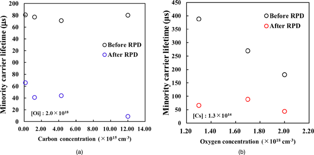
Fig. 1. (Color online) Relation between Cs/Oi concentration and minority carrier lifetime before and after RPD process with (a) oxygen concentration (b) carbon concentration.
Download figure:
Standard image High-resolution imageSubsequently, we evaluated the plasma induced defects after RPD process by PL measurement. Here, to evaluate the damage into silicon substrate, the PL measurement was similarly performed on the samples in which the ITO film deposited by RPD method was removed. Figures 2 and 3 shows the PL spectra before and after the RPD process, respectively. The peak due to band edge emission and phonon replica were clearly observed at around 1.1 eV. The peak was observed in the deep level region of 0.79 eV for each sample after the RPD process while it was not observed from the substrate without RPD (as-grown). This suggests that the plasma irradiation induced a deep level emission line. This deep level emission line can be assigned as C-line, which is originated from the radiation-induced defects of the interstitial carbon (Ci) and interstitial oxygen (Oi) complexes (Ci–Oi).30–32) That is, it is suggested that the main cause of the lifetime degradation on the silicon substrate is Ci–Oi defects originated by plasma irradiation during the RPD process.

Fig. 2. PL spectra of as-grown sample.
Download figure:
Standard image High-resolution image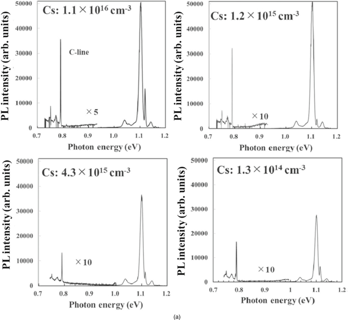
Download figure:
Standard image High-resolution image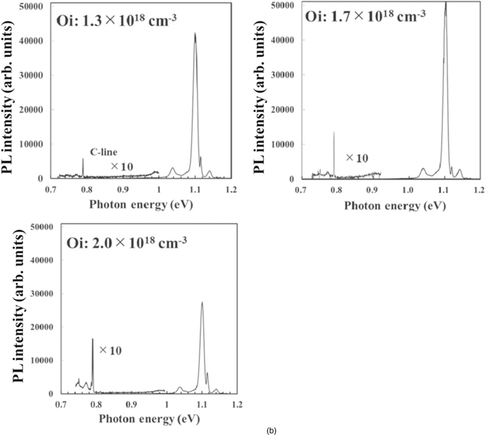
Fig. 3. PL spectra after RPD process with (a) oxygen concentration of 2.0 × 1018 cm−3 (b) carbon concentration of 1.3 × 1014 cm−3.
Download figure:
Standard image High-resolution imageIt has been reported that the origin of the Ci–Oi defect is kick out Ci formation caused by electron or energy particle.32) Although various factors may be considered for the defect formation of the substrate in the plasma process, we presume that electron and ion can contribute to the pushing of Si atoms into the interstitial lattice, and then Ci is kicked out. However, further studies are needed to reveal in detail factors that cause defect formation.
Also, we have confirmed that C-line intensity is closely related to minority carrier lifetime after RPD process. Figure 4 shows that the C-line intensity is high when the lifetime is low. Therefore, there is the possibility that the number of defects introduced by plasma irradiation on silicon substrate differs depending on the impurity concentration, even at the same irradiation energy. From these results, we revealed that in RPD process, Ci–Oi defects are formed by plasma irradiation, resulting in lifetime degradation on Si substrate.

Fig. 4. (Color online) Relationship between C-line intensity and minority carrier lifetime.
Download figure:
Standard image High-resolution imageFurthermore, we evaluated the depth profile of irradiated defects in the substrate with step etching by HNO3, CH3COOH and HF mixture (HNO3:CH3COOH:HF = 40:15:1). The etching cycle was repeated with one dipping for 5 s in the solution followed by flowing deionized water. Figure 5 shows the relationship between the C-line intensity and minority carrier lifetime dependence of the etching depth in the sample with low carbon (1.3 × 1014 cm−3) and oxygen (1.3 × 1018 cm−3). One etching cycle corresponds to approximately 1 nm depth, which was estimated from 1 μm etching time. From Fig. 5, the minority carrier lifetime was gradually improved by etching, approached to the same value as the as-grown sample. In addition, we have confirmed that the C-line intensity decreases with the improvement of the lifetime on the silicon substrate. Therefore, it is considered that high density recombination centers exist near the surface of the silicon substrate within approximately 100 nm from the surface. Also, it has been clarified that the origin of the defects which cause in the lifetime degradation of the silicon substrate by plasma irradiation is Ci–Oi defects.
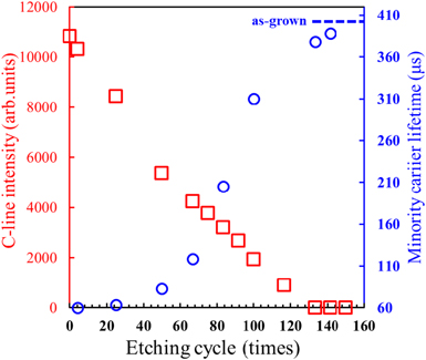
Fig. 5. (Color online) Relationship between C-line intensity and minority carrier lifetime dependence of the etching depth with carbon (1.3 × 1014 cm−3) and oxygen (1.3 × 1018 cm−3).
Download figure:
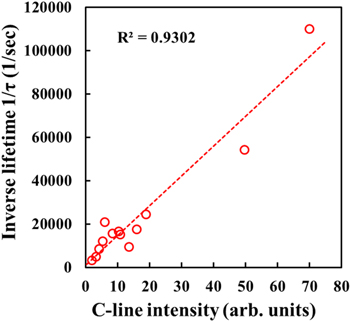
Standard image High-resolution imageWe investigated the correlation between the C-line intensity obtained after the RPD process and the minority carrier lifetime. From Fig. 6, the minority carrier lifetime drastically decreased according to the C-line. Here, we assume that the C-line intensity is correlated with the density of Ci–Oi defects. Figure 6 suggested that these are proportional relation. Although correlation coefficient of R2 = 0.93 proves there is a strong correlation between C-line intensity and 1/τ. One may anticipate slight deviation especially in the low C-line intensity region. This may be attributed to the fact that it is usually hard to reproduce low PL intensity completely. The difference of the other defects such as meta impurities, oxygen precipitates, or dangling-bond caused by strain may affect somehow. However, the major origin of the lifetime degradation by the RPD process is most likely attributed to the Ci–Oi defects formation.
Fig. 6. (Color online) Correlation between the C-line intensity after the RPD process and the minority carrier lifetime.
Download figure:
Standard image High-resolution image
The effective minority carrier lifetime is expressed as

where, τsurface, τsub-surface and τbulk is the surface, sub-surface and bulk recombination lifetime, respectively.
From Fig. 5, the high density recombination center exists approximately 100 nm from the Si substrate surface. Therefore, sub-surface recombination is more dominant than bulk: 1/τsub-surface ≫ 1/τbulk and Eq. (1) can be expressed as

where, Shockley–Read–Hall recombination characterized by the lifetime τSRH, radiative recombination characterized by τRad and auger recombination characterized by τAuger.31)
The minority carrier recombination rate Utotal is expressed as

The total recombination ratio Utotal and the SRH recombination ratio USRH due to impurities and defects are expressed as

where W is the wafer thickness and Δn is the excess carrier density

where σn and σp are the cross sections of electrons and holes, νth is the thermal velocity of electrons, and Nt is the defect density.10,33) Also, n is the electron density, p is the hole density, and n1 and p1 are variables related to the recombination rate depending on the energy Et of the trap level. That is, the following equation is given from the Eqs. (3)–(5) by using the arbitrary constant a representing the bulk recombination components, and the constant b representing the surface recombination and other recombination components

Assuming that NCi–Oi is the density of Ci–Oi defects and Nt = NCi–Oi, Eq. (7) expressed as

Equation (7) implies that the inverse lifetime is proportional to the Ci–Oi defect density, and we have experimentally shown that it is correct. Hence, the relation coefficient of the graph was R2 = 0.93 and it can be concluded that the density of Ci–Oi defects and the minority carrier lifetime showed good correlation and the Ci–Oi defects is a dominant carrier recombination center. We can also conclude that the Ci–Oi defects are the SRH recombination centers. The surface defects are usually composed of dangling-bond without termination. Thus, we recognized Ci–Oi defects as bulk defects rather than surface defects. However, Ci–Oi defects are confined in the relatively close to the surface (−100 nm), which may also affect the small deviation in the low C-line intensity region of Fig. 6.
From these results, we have demonstrated that the plasma process used in solar cells fabrication such as the RPD method originates defects formation in the silicon substrate and reduces the minority carrier lifetime. In addition, PL spectroscopy identity the origin of the irradiation defect was a defect derived from impurity carbon and oxygen, namely a Ci–Oi defect. These defects were stable even after 200 °C 20 min annealing which is simulating the low temperature electrode fabrication process. It is also presumed that this type of defects can be produced through low density a-Si: H layer with several tens nano-meter even in the actual device process. Therefore, it is important to control this type of defect on the silicon substrate during the process to increase the cell efficiency. This should be able to be achieved by reducing O and C impurities and/or plasma damage.
4. Conclusions
Plasma irradiation defects on silicon substrates during the solar cell process were evaluated by minority carrier lifetime and PL spectroscopy. Plasma irradiation introduces some defects into the silicon substrate and significantly reduces the minority carrier lifetime. Therefore, we revealed that the cause of the lifetime degradation on the silicon substrate is Ci–Oi defects originated by plasma irradiation during the RPD process. There was a correlation between these defects and minority carrier lifetime degradation by plasma irradiation. In addition, the etching depth profile showed that these defects were exist at high density on the substrate surface. From the above, the plasma process such as the RPD method in solar cell fabrication may introduces defects that degrade the cell performance to the silicon substrate. Therefore, in order to achieve high efficiency, efforts to control irradiation defects such as Ci–Oi defects are required.
Acknowledgments
This research was conducted with the support of New Energy and Industrial Technology Development Organization. We would like to thank Dr. Michio Tajima, Meiji University, for his advice on the PL characterization.