
Abstract
Photoelectron spectroscopy resolved in three-dimensional momentum space with a microscopic field of view is realized by combining a so-called Momentum Microscope with a soft X-ray synchrotron radiation source. A new experimental station for momentum-resolved photoelectron micro-spectroscopy and spectro-microscopy has been built at BL6U, an undulator-based soft X-ray beamline of the UVSOR synchrotron facility. This experimental station specializes in characterizing the electronic structure of surface atomic sites, thin films, molecular adsorbates, and bulk crystals. The instrument details are described along with possible measurement techniques.
Export citation and abstract BibTeX RIS

Content from this work may be used under the terms of the Creative Commons Attribution 4.0 license. Any further distribution of this work must maintain attribution to the author(s) and the title of the work, journal citation and DOI.
1. Introduction
Based on the principle of energy and momentum conservation in the photoemission process, momentum-resolved photoelectron spectroscopy provides a wealth of information about the electronic and atomic structure of solids and surfaces.1)
The angle-integrated photoelectron energy distribution curve reflects the density of states of valence bands. The behavior of valence electrons and the interference of photoelectrons are projected onto the momentum space as an angular distribution pattern of photoelectrons. By measuring a series of two-dimensional (2D) photoelectron angular distributions as a function of binding energy and photon energy, one can map the valence band dispersion and Fermi surface of a crystal in three dimensions (3D). The arrangement of atomic orbitals in the momentum space and their linear combination coefficients in the real space can be determined by analyzing the transition matrix elements2–4) and the photoelectron structure factor.5–7) The molecular orbitals of the oriented π conjugate adsorbates on the surface were visualized based on photoelectron orbital tomography techniques.8–12)
Photoelectrons from the localized core levels are excellent probes for element-specific atomic structure analysis. Photoelectron diffraction is the result of quantum mechanical interference between element-specific photoelectron waves emitted from X-ray excited atoms and scattered waves from surrounding atoms. Much effort has been put into the development of atomic structure analysis methods based on photoelectron diffraction.13–17) Since diffraction patterns differ according to the atomic arrangements surrounding excited atomic sites, such atomic-site-specific information can be "fingerprinted" by their characteristic diffraction patterns. These diffraction patterns, combined with spectroscopy, can be used as atom-site resolution probes for local electronic structure investigations.18–20)
Since surface compositions and structures tend to differ from bulk crystals, it is important to comprehensively study their atomic structure and electronic properties. Therefore, efficient valence-band and core-level photoelectron angular distribution measurements from the same position on the surface are important techniques in materials science. Photoelectron spectroscopy, resolved in 3D momentum space with a microscopic field of view (FoV), is realized by a combination of a so-called Momentum Microscope (MM)21–27) and a soft X-ray synchrotron radiation source. A new experimental station for momentum-resolved photoelectron micro-spectroscopy and spectro-microscopy has been built at BL6U of the third-generation synchrotron radiation source, UVSOR-III. BL6U is an undulator-based soft X-ray beamline.28,29) MM is a device that combines a photoemission electron microscope (PEEM) lens, an imaging-type energy analyzer, and a 2D position-sensitive electron detector. In the current case, a hemispherical deflection analyzer (HDA) is used for energy filtering. This experimental station is dedicated to the characterization of the electronic structure of not only substrate crystals but also local atomic sites on the surface, epitaxial thin films, and oriented molecular adsorbates. In the case of soft X-ray excitation, since the escape depth of photoelectrons is less than a few nanometers,30) it is possible to analyze the electronic structure and local atomic arrangement on the crystal sample surface sensitively. Details of the instrument are described along with possible measurement techniques and applications.
2. Technical details
2.1. Momentum Microscope
The conventional approach to study the electronic and atomic structure of small-crystalline and multi-domain-structure samples is to focus an X-ray beam onto a selected area. For the 2D photoelectron angular distribution measurements, a display-type spherical mirror analyzer (DIANA) with a large acceptance solid angle of 1π steradian (±60°) is one of the most efficient apparatus.31–34) The 2D angular distributions of the specific kinetic energy photoelectrons and Auger electrons emitted from the sample are projected onto the fluorescent screen. Recently, several new designs have been developed using an ellipsoidal mesh lens to achieve better energy resolution35–37) and a wider acceptance angle of 2π steradians at kinetic energy up to 1 keV.38) By combining a focused soft-X-ray beam together with a sample position scanning mechanism, scanning microscopic photoelectron spectroscopy and diffraction measurements from small and/or polycrystalline samples were realized.39) HDAs are widely used to measure energy and angular dependence of photoelectron intensity (binding energy Eb versus wave number k) for angle-resolved photoelectron spectroscopy (ARPES). In this case, rotation of the sample orientation is required to cover a wide solid angle. This results in a longer acquisition time and a shift of the measurement position of the sample. Input lenses with deflectors were developed for the photoelectron angular distribution measurements from the fixed irradiated spot on the sample surface.28,29,40) In the synchrotron radiation facility, Fresnel zone plates are used as focusing optics with an HDA with a deflector to realize ARPES measurements on the submicrometer scale. Energy resolution and FoV achieved are 50 meV and 120 nm at ALS BL 7.0.2 (photon energy: 80–1000 eV),41) 30 meV and 700 nm at DIAMOND I05 (60–150 eV),42,43) 25 meV and 150 nm at Soleil ANTARES (95–1000 eV)44) and 12.5 meV and 500 nm at Elettra Spectromicroscopy beamline (27 and 74 eV).45) However, some samples, such as compound materials and organic molecular films, are fragile and can still easily be degraded by such intense focused X-ray irradiation.
wAnother approach to efficiently obtain wide-range 2D angular distribution is the use of a cathode lens46,47) together with an imaging-type energy analyzer. A high acceleration voltage of typically 10–30 kV is applied between the sample and the entrance of the objective lens. This technique has been used in PEEM48–50) and related instruments including an energy-filtered PEEM,51) SPELEEM,10,49,52) NanoESCA,53) and MM.23–25) The accelerated electrons are decelerated and energy filtered by a retarding-grid analyzer,51) a band-pass analyzer such as HDA,23–25,52–54) or a time-of-flight analyzer.55–58) Here, the full acceptance angle of 2π steradian is realized for photoelectron kinetic energies Ek up to some tens of eV. Acquisition times of x–y images and kx–ky patterns are significantly reduced by using an imaging type energy analyzer. The Elettra NanoESCA beamline has a double-HDA-type MM in operation with spatial and energy resolutions of 50 nm and 100 meV at 30 K, respectively.59) This MM is equipped with a 2D spin filter for acquiring spin-resolved textures in both real and reciprocal space.60)
At BL6U, the first newly developed single-HDA-type MM, KREIOS 150 MM (SPECS), is installed. The energy resolution is improved and temperatures below 10 K are reachable. As shown in Fig. 1, this system consists of a PEEM lens, a HDA, a 2D position-resolved detector, and a complementary MOS (CMOS) camera. A hexapod sample stage with a cooling capacity down to below 10 K has been developed for precise sample alignment and is now commercially available from SPECS as HESTIA. The normal direction of the sample surface must be exactly aligned with the lens axis. The working distance between the sample and the PEEM lens is 4.0 mm. The sample surface is part of the cathode lens together with the entrance of PEEM as the counter electrode. Extraction voltage of 10–20 kV is applied between the sample surface and the entrance of the PEEM lens. Additional positive adjustment voltage corresponding to the kinetic energy of the emitted electron to be analyzed is applied to the sample. The photoelectron kinetic energy is measured from the vacuum level, which is defined as the potential of the analyzer work function added to the Fermi level of the sample surface. Note that the definition of photoelectron kinetic energy is independent of the bias voltage and this additional adjustment voltage.
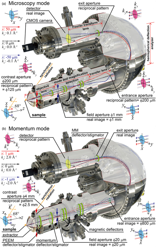
Fig. 1. (Color online) Schematic diagram of the Momentum Microscope consisted of a PEEM lens, a HDA, a 2D position sensitive detector, and a CMOS camera. (a) Microscopy mode. (b) Momentum mode. The definitions of the real and reciprocal coordinates used in this article are indicated. The electron trajectory inside the PEEM lens are expanded along x axis.
Download figure:
Standard image High-resolution imageThe first PEEM lens tube (objective lens) is used to process the photoelectrons through the contrast and field apertures. This lens part keeps a constant type of display so that the reciprocal space (back focal) plane and real space (Gaussian) plane are located at constant positions of the contrast and field apertures, respectively. The second PEEM lens tube is responsible for refocusing the electrons onto the exit of the lens to generate either real space (x, y) images or reciprocal space (kx, ky) patterns. Furthermore, the magnification can be varied. The size of the FoV in the real and the reciprocal spaces for the momentum and microscopy modes, respectively, are determined by the acceptance cone (±1.5°) of HDA. The details of the PEEM lens are given by Tusche et al.24) Table I shows the maximum FoV size for each magnification parameter (arbitrary unit) in the current system.
Table I. The maximum size of field of view (FoV) for each magnification parameter. The extraction voltage is set to 15 kV.
| Magnification parameter | Real space FoV | Reciprocal space FoV |
|---|---|---|
| 1.0 | ϕ200 μm | ±3.2 Å−1 |
| 2.0 | ϕ100 μm | ±2.0 Å−1 |
| 3.0 | ϕ50 μm | ±1.0 Å−1 |
| 4.0 | ϕ20 μm | ±0.5 Å−1 |
| 5.0 | ϕ10 μm | ±0.25 Å−1 |
The HDA is fixed so that the axis connecting the entrance and exit apertures are aligned vertically. The real space x axis and the reciprocal space kx axis at the sample surface are defined parallel to this vertical line, which is in the vertical plane containing the axis of the PEEM, and the centers of the entrance and the exit apertures. The y axis is orthogonal to the x axis. The HDA works as an energy filter with an imaging function. This filter is made so that only those electrons will reach to the HDA exit aperture, which have particular energies within a range around the pass energy, Epass. The 2D real space image or reciprocal space pattern at the entrance aperture position is reproduced at the exit aperture position. HDA entrance aperture and exit aperture pairs of the same diameter can be selected. The electrons that arrive at the HDA exit aperture pass through a Fourier transform lens. This lens performs a Fourier transform (from real space to reciprocal space or vice versa) in the detector section. The 2D intensity data projected on the screen is captured by the CMOS camera.
Electron trajectory for PEEM (microscopy mode) and momentum-resolved photoelectron spectroscopy (momentum mode) measurements are shown in Figs. 1(a) and 1(b), respectively. The extraction voltage, the electron kinetic energy, and the magnification parameter are set at 15 kV, 16 eV, and 2.0, respectively. In the case of microscopy mode, the maximum acceptance cone size of HDA corresponds to the FoV of 100 μm in diameter. The real and reciprocal coordinate systems at the sample surface position are defined so that the x and kx axes point upward parallel to the line connecting the entrance and exit apertures of HDA. The electron trajectories emitted from the x position of ±50 μm are indicated by red and blue arrows, while those of the electrons having kx momentum of ±0.1 Å−1 are indicated by solid and dotted arrows. The diameter of the reciprocal space pattern at the contrast aperture position and the real space image at the field aperture position are 125 μm and 1 mm, respectively. The real space image of the sample surface is transformed to reciprocal space pattern of 200 μm in diameter at the HDA entrance aperture position. The contrast aperture of 200 μm in diameter and the field aperture of 1 mm in diameter fit to these trajectories. By limiting the electron emitted at the surface normal direction by the narrower contrast aperture of 100 μm in diameter, the spatial resolution will be improved.
In the case of momentum mode with the extraction voltage of 15 kV and the magnification parameter of 2.0, the maximum acceptance cone (±1.5°) of HDA limits the momentum FoV of PEEM lens to ±2.0 Å−1. The electron trajectories emitted from the x position of ±1 μm are indicated by red and blue arrows, while those of the electrons having kx momentum of ±2.0 Å−1 are indicated by solid and dotted arrows. The diameter of the reciprocal space pattern at the contrast aperture position and the real space image at the field aperture position are 2.5 mm and 20 μm, respectively. By limiting the electron emitted from the small area by the field aperture, the momentum resolution will be improved. The real space image of the sample surface is projected at the HDA entrance aperture position. The diameter of the real space image at the HDA entrance aperture position is 800 μm. Note that the electrons having kx momentum of ±2.0 Å−1 are partially blocked by the HDA aperture of 0.5 mm × 1 mm.
The system is equipped with several sets of single spot shifting lenses at different locations on the PEEM axis of which one deflector or stigmator is used at a time to manipulate the electron beam. PEEM deflectors can be used to center the region of interest at the detector without moving the sample. The best crystalline quality position on the sample can be searched by comparing the contrast of the valence band dispersion patterns or the core-level photoelectron diffraction patterns in momentum mode while scanning PEEM deflectors. Momentum deflectors are used to select the region of interest in the reciprocal space. The contrast aperture is used to refine the area of interest to a specific point in the reciprocal space in microscopy mode (dark field imaging). The field apertures is used to refine the area of interest in the real space in momentum mode (micro-ARPES). To increase the energy resolution, smaller apertures at the HDA entrance and exit are used. Note that at the same time, the entrance aperture acts as a field aperture for momentum mode and as a contrast aperture for microscopy mode. The size of the PEEM and HDA apertures are listed in Table II.
Table II. The size of apertures. A pair of HDA entrance and exit apertures with same diameter can be selected. The rectangular apertures marked with asterisk (∗) are for the conventional ARPES mode (Eb, k) usage.54)
| Contrast apertures | Field apertures | HDA apertures |
|---|---|---|
| ϕ4 mm | ϕ4 mm | ϕ6 mm |
| ϕ4 mm with grid | ϕ4 mm with grid | ϕ4 mm |
| ϕ300 μm | ϕ2 mm | ϕ2 mm |
| ϕ200 μm | ϕ1.5 mm | |
| ϕ100 μm | ϕ1 mm | 1 mm × 1.8 mm |
| ϕ500 μm | 0.5 mm × 1 mm | |
| ϕ250 μm | 0.2 mm × 0.8 mm | |
| ϕ100 μm | ||
| ϕ50 μm | 0.25 mm × 25 mm∗ | |
| ϕ20 μm | 0.05 mm × 25 mm∗ | |
2.2. Beamline optics
BL6U is an entrance-slit-less design to obtain the high photon flux. In-vacuum undulator U6 generates horizontally-linearly-polarized soft X-ray. The variable-included-angle Monk–Gillieson mounting monochromator with a varied-line-spacing plane grating covers photon energy range of 40–800 eV, with the resolving power E/ΔE of 5000–10 000 and the photon flux of 109–1011 ph s−1. Typical width of an exit slit is 2–50 μm in vertical direction. A refocusing mirror of 1:1 convergence focuses the monochromated soft X-ray onto the sample position. A four-quadrant beam position monitor is provided to maintain the soft-X-ray beam at the focused position of the analyzer. As shown in Fig. 2, the axis of PEEM lens is set 68° off from the incident X-ray beam direction. The final footprint of irradiation spot is 300 μm in horizontal direction and 2–50 μm in vertical direction.
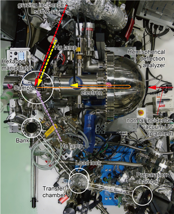
Fig. 2. (Color online) Topview photograph of the experimental station composed of a Momentum Microscope analysis chamber, a bank chamber, a transfer chamber, a load lock chamber and a preparation chamber.
Download figure:
Standard image High-resolution imageBy adding a second HDA to the current single HDA MM system, the energy resolution can be improved in the double dispersion mode.26) HDA is equipped with an access port at the PEEM lens axis for checking the position of entrance aperture. For the future extention, introduction of polarization variable synchrotron radiation or laser beam introduced through this port at normal incident geometry is planned. In this case, the contrast and field apertures as well as the HDA entrance aperture are opened to let the beam go through. The high spatial, momentum, and energy resolution measurements are achieved by using a small exit aperture in the first HDA and by adding the second HDA.26)
2.3. Experimental station
As shown in Fig. 2, the experimental station includes an analysis chamber with a MM, a bank chamber, a transfer chamber, a load lock chamber, and a preparation chamber. The MM chamber is also equipped with mercury (Hg) and helium (He) lamps positioned at the 68° off direction from the PEEM lens axis.
The sample stage facing to the PEEM lens is controlled by a hexapod and has six axis of freedom; (x, y, z, tiltx, tilty, ϕz) = (±5.5 mm, ±5.5 mm, ±2.5 mm, ±5°, ±5°, ±70°). The stage can be retracted to let the excitation beam pass through for beam adjustment. Samples can be cooled down below 10 K and heated up to 400 K. The sample stage temperature measured at the Cu block directly contacting with the sample holder was 5.6 K. The actual sample temperature measured at the sample holder was higher than that at the Cu block by about 3.1 K. During the cooling procedure, the shift of the sample position was within 10 μm.
The preparation chamber is equipped with a sample heating and cooling stage, an ion gun, LEED and RHEED optics, sample holder garages, and ports for evaporators and gas dosages.
3. Analyzer performance
The details of the specification evaluation result are described below.
3.1. Spatial resolution and field of view
The size of the FoV is determined by the field aperture size and the magnification parameter. Figure 3 is a Si wafer with a gold patterned thin film imaged by using a Hg lamp with a large FoV with diameter of about 150 μm. The dark squares correspond to the gold pattern with an area of 100 μm2. Each square is composed of a smaller checkered pattern of 10 × 10, and the area of each pixels is 1 μm2. Photoelectrons with a kinetic energy of almost 0 eV were imaged. Note that the area patterned with gold has a lower emission current compared to the Si substrate area in this measurement condition.
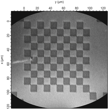
Fig. 3. Gold checkerboard pattern observed using 2000 μm aperture, magnification parameter 1.0, and extraction voltage of 15 kV. The size of each square is 100 μm2. Note that the gold patterned area have lower emission current compared to the Si substrate area in this case.
Download figure:
Standard image High-resolution imageThen the spatial resolution in the microscopy mode was evaluated. The size of the contrast aperture (or k-field aperture) listed in Table I can be selected. The smaller the size, the better the contrast of the PEEM image and the better the spatial resolution are achieved. An enlarged image of this gold checkered pattern is shown in Fig. 4. A gold square island with an area of 1 μm2 and a thickness of 150 nm was arranged in a checkerboard pattern of 10 × 10. The kinetic energy of the photoelectrons was 150 meV. The pass energy was set at 20 eV and the photoelectrons were extracted by a PEEM lens. The magnification parameter was 5.0. The gold squares are observed brightly. Judging from the intensity cut off at the square edge of the gold, the spatial resolution of the instrument was demonstrated to be about 50 nm. We found that the contrast of the gold checkerboard pattern image excited by the Hg lamp is not trivial. The gold pattern region is brightly imaged with kinetic energy of 150 meV, but the contrast of the gold pattern with kinetic energy of almost 0 meV is reversed. One possible explanation is that the density of states in the gold pattern region at the Fermi level is higher than that in the Si substrate region, while the work function in the gold pattern region is higher than that in the Si substrate region.

Fig. 4. (Color online) (a) Gold checkerboard pattern observed by microscopy mode using Hg lamp as excitation. The size of each square is 1 μm2. (b) The red curve is the intensity profile of the area indicated by two red lines in (a). The blue curve is the first derivative of the red curve. Spatial resolution is shown to be around 50 nm.
Download figure:
Standard image High-resolution image3.2. Energy resolution
Energy resolution was evaluated by measuring the Fermi edge of graphene on Ru sample using He I light (21.2 eV) for excitation. Pass energy was set at 20 eV. The entrance aperture size of HDA was 0.2 mm × 0.8 mm. The energy spectrum measured in momentum mode shows that the total energy resolution was 22.78 meV. The sample temperature was 9 K. The resolution of the analyzer is estimated to be 22.74 meV by taking into account the contribution of the He light source energy width of 1 meV and the thermal spread of 0.78 meV.
3.3. Momentum resolution
The radius of the photoemission horizon used for momentum calibration is defined by the kinetic energy Ek (in eV)

The maximum possible k-FoV radius is 3.2 Å −1 with the magnification parameter of 1.0. If  is larger than the maximum allowed k-FoV radius,
  , determined by the extraction voltage, photoelectron kinetic energy, and magnification parameter, the photoemission horizon falls out of k-FoV. For example, photoelectrons emitted in all hemisphere directions can be detected with a kinetic energy of up to 39.0 eV. For a kinetic energy above 39.0 eV, the detection acceptance cone is limited by
  . The maximum emission angle α is determined as follows

The field aperture in the real space plane of the PEEM lens refines the real space FoV to perform photoelectron spectroscopy from a defined small space. The smallest field aperture of 20 μm corresponds to a FoV diameter of 2 μm. The diameter of FoV decrease from 1/8 to 1/12 of the diameter of field aperture, as the extraction voltage increases. The ultimate momentum resolution is designed to be less than 0.01 Å−1.
Momentum-resolved valence band dispersion spectra of monolayer graphene on Ru(111) surface were measured using He I light (21.2 eV). Figure 5(a) shows an isoenergy cross section near the Fermi level. The kinetic energy was 16.0 eV. The magnification parameter has been set to 2.0. The acquisition time was 222 s. Six bright spots forming a hexagon and two ring structures around the center correspond to the graphene π and Ru 4d bands, respectively. Figure 5(b) shows the enlarged view near the Dirac point in the K direction indicated by blue rectangle region Fig. 5(a). Note that the pattern is rotated 90° counterclockwise. The magnification parameter has been set to 4.0. Momentum resolution was evaluated from the cut off of the photoemission horizon measurement. As shown in Fig. 5(c), the intensity profile shows that, in this case, a momentum resolution of 0.012 Å−1 has been achieved. We evaluated the momentum resolution in the x direction where the effect of aberrations is not zero. Momentum resolution along the y direction should be similar or better, since aberration effects are negligible in this direction.

Fig. 5. (Color online) (a) Isoenergy cross section of the valence band dispertion of graphene on Ru(111) surface and (b) the closeup around the Dirac point at K direction indicated by blue rectangle in (a). (c) Momentum resolution was evaluated from cut-off of photoemission horizon measurement observed by momentum mode using He-I light (21.2 eV) as excitation. Kinetic energy was 16.0 eV. The red curve is the intensity profile of the area indicated by two red lines in (b). The blue curve is the first derivative of the red curve. Intensity profile indicate that the momentum resolution of 0.012 Å−1 is achieved.
Download figure:
Standard image High-resolution image4. Measurement methods and applications
4.1. Photoelectron microscopy measurements
Figure 6(a) shows the gold checkerboard pattern observed in microscopy mode using the Hg lamp. The size of the smallest square is 1 μm2 and the size of the 10 × 10 checkerboard pattern is 100 μm2. The same area was excited by synchrotron radiation and microscopic image was acquired. The photon and kinetic energies were set at 110 eV and 21.3 eV, respectively, to detect Au 4f7/2 photoelectron peak. The exit slit of the beamline monochromator was 10 μm. Figure 6(b) shows that this focused X-ray beam excited a width of about 15 μm region. Note that the gold squares excited by the X-ray beam were brightly imaged. For synchrotron micro-spectroscopy and spectro-microscopy measurements, fine X-ray beam and sample surface alignment and stabilization at the focal point of the PEEM lens is essential.
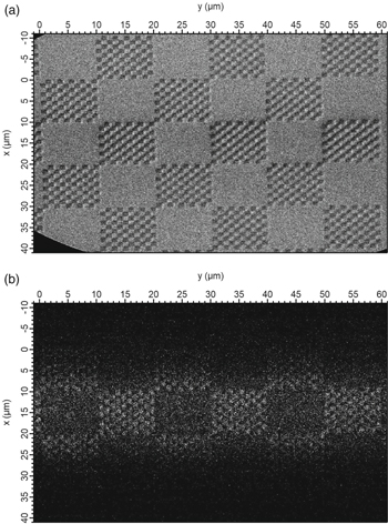
Fig. 6. Gold checkerboard pattern observed by microscopy mode. The size of the smallest square is 1 μm2 in area. (a) Photoelectron at the vicinity of vacuum level threshold excited with the Hg lamp. (b) Au 4f photoelectron excited with synchrotron radiation. Photon energy and kinetic energy was 110 eV and 21.3 eV, respectively.
Download figure:
Standard image High-resolution imageAn essential condition for measurement with a cathode lens analyzer is the macroscopic flatness of the sample surface. The aspect ratio of the gold checkerboard pattern was 1 μm in the lateral direction to 150 nm in the height direction. Figure 7 shows the optical and PEEM images of the honeycomb pattern sample. A piece of micro channel plate (MCP) fragment was fixed to the sample holder with a 0.3 mm thick Ta plate. The pore size was 10 μm and the interval of each pore was 11.6 μm. The top surface of the MCP is clearly imaged, despite the nearby deep holes. It is interesting to note that excited photoelectrons are detected from one side of the hole wall. Distorted images were acquired when the Ta plate was located within 1 mm of the observation point.

Fig. 7. (Color online) (a) Photograph and (b) PEEM image of a honeycomb patterned sample. The Hg lamp was used as the excitation source. The white bar in (a) indicates the length of 10 μm. The interval of each pore is 11.6 μm.
Download figure:
Standard image High-resolution image4.2. Valence band dispersion mapping measurements
Figure 8 shows the valence band dispersion of monolayer graphene on the Ru(111) surface measured by synchrotron radiation. The photon energy was 50 eV. The total acquisition time for a series of momentum resolved data, i.e. 61 isoenergy patterns from 46.0 to 40.0 eV, was one hour. The left panels correspond to the valence band isoenergy cross sections at kinetic energies of 45.0, 43.0, and 41.0 eV from the top. Right panels show E–k cross section along  and
and  directions. The π band is clearly visible in the first Brillouin zone but less bright in the second Brilluoin zone. The σ band is observed in the second Brillouin zone. These differences in intensity are due to the photoelectron structure factor effect.5–7) The photoelectron intensity distribution is expected to be symmetric respect to the kx = 0 line. However, the intensity of the positive region of kx is partially depressed. This is probably due to the cryogenic shield of the manipulator, which blocked photoelectrons in the corresponding direction. This problem is solved by optimizing the path of the synchrotron beam and the height of the sample mounted on the sample holder plate.
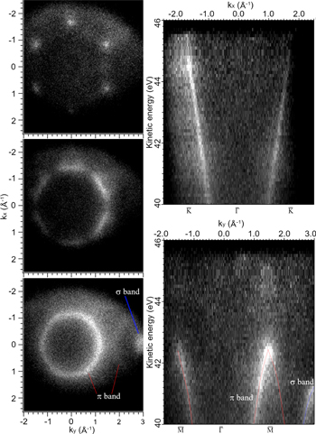
Fig. 8. (Color online) Valence band dispersion of the graphene on the Ru(111) surface measured with synchrotron radiation. Photon energy was 50 eV. Left panels correspond to the isoenergy cross section of valence band at the kinetic energy of 45.0, 43.0 and 41.0 eV. Right panels correspond to the E–k cross section along  and
and  directions.
Download figure:
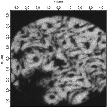
Standard image High-resolution imageThe PEEM image from the same area of the momentum mode measurement described above is shown in Fig. 9. The magnification parameter has been set to 4.0. The steps appeared as dark curves, while most of the terraces appeared to be of uniform contrast, suggesting that they were evenly covered with an epitaxial graphene layer.
Fig. 9. PEEM image of the graphene on the Ru(111) surface measured with synchrotron radiation. Photon energy was 50 eV. The magnification parameter was set to 4.0.
Download figure:
Standard image High-resolution image
The acquisition time for valence band dispersion mapping can be reduced by increasing the photon flux density or increasing the size of FoV. The latter method is effective for measuring samples that are vulnerable to X-ray irradiation.
4.3. Core level spectroscopy
Acceptance angle α for  Å−1 correspond to the angle of 30° for 156 eV and 15° for 582 eV. This acceptance cone range is sufficient to perform photoelectron diffraction in energy scan mode and is useful for analyzing local surface adsorbate structures.61) However, this is not enough for 3D atomic arrangement reconstruction by photoelectron holography, which requires a wide solid angle intensity distribution data. Increasing the extraction voltage can increase the acceptance angle to some extent. In order to collect photoelectrons beyond the k-FoV limit, it is necessary to reshape the extractor to make the opening larger.38)
With a photon energy range up to 800 eV covered by the BL6U, core-level excitation of a variety of important elements is possible. Resonant momentum-resolved photoelectron spectroscopy is a promising method that opens the door to elemental- and orbital-selective valence band dispersion mapping. Comprehensive investigation of the occupied and unoccupied electronic structures on the sub-μm scale is enabled by X-ray absorption spectroscopy by Auger electron detection in microscopy mode combining with dark field imaging of valence band dispersion.
5. Summary
Photoelectron spectroscopy resolved in 3D momentum space with a microscopic FoV is achieved by a combination of the so-called MM and a soft X-ray synchrotron radiation source. The latest version of MM system has been installed at the undulator-based soft X-ray beamline BL6U of the UVSOR synchrotron facility. A new experimental station for momentum-resolved photoelectron micro-spectroscopy and spectro-microscopy has been built. The real space microscopic images and 2D momentum-resolved photoelectron patterns can be acquired from the same position of the sample surface. This experimental station is dedicated to the electronic structure characterization of local atomic sites on surfaces, thin films, molecular adsorbates, and bulk crystals. The details of the instrument and the preliminary results are described along with possible measurement techniques.
Acknowledgments
We greatly acknowledge Dr. Markus Breusing, Dr. Marko Wietstruk, and Dr. Mirko Weidner (SPECS) and Dr. Dai Yamaguchi (Tokyo Instruments Inc.) for their contribution in the construction of the BL6U Momentum Microscope experimental station. The electron trajectory simulation used in Fig. 1 and the spatial and momentum resolution evaluation data shown in Figs. 3–5 were provided by SPECS as part of the factory acceptance test. F. M. and S. K. acknowledge Dr. Christian Tusche and Prof. Claus M. Schneider (Forschungszentrum Jülich, PGI-6) for their valuable advice through the framework of international collaboration between Forschungszentrum Jülich and Institute for Molecular Science (IMS). This study was partly supported by Grants-in-Aid (19KK0137, 18H03904, and 17H02911) from the Ministry of Education, Culture, Sports, Science, and Technology, Japan. The optical photograph shown in Fig. 7(a) is provided by Dr. Takuya Ohigashi (IMS).