
Abstract
Wide-bandgap semiconductor devices, such as gallium nitride and silicon carbide devices, have attracted great interest in the automotive application area. However, wide-bandgap semiconductor devices are still too expensive to apply in the power electronics system in automotive applications. In this application, the series-connected active power semiconductor device method using low voltage rating power semiconductor devices of power conversion systems is an effective solution for the cost and efficiency problems. However, there exists no discussion about the voltage imbalance phenomenon for series-connected active power semiconductor devices. In this paper, the voltage imbalance phenomenon is analyzed and evaluated using simulation and an experimental setup in the case of a hard-switching DC–DC converter and a soft-switching one suitable for automotive applications.
Export citation and abstract BibTeX RIS

Content from this work may be used under the terms of the Creative Commons Attribution 4.0 license. Any further distribution of this work must maintain attribution to the author(s) and the title of the work, journal citation and DOI.
1. Introduction
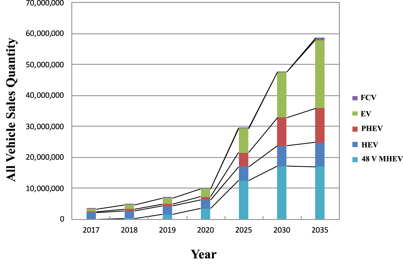
In 2020, the automotive application area is faced with strict EU regulation of exhaust gas1) as shown in Fig. 1. The regulation amount of carbon dioxide emission is 95 g km−1 for each auto manufacturer. This is not just a regulation but every manufacturer's responsibility to the global environment to combat global warming. To overcome this regulation hurdle, each auto manufacturer will have to produce several types of xEVs (including electric vehicles, hybrid electric vehicles, mild hybrid electric vehicles, and fuel cell electric vehicles) in the future. In this paper, electric vehicles are referred to as EVs, hybrid EVs as HEVs, mild HEVs as MHEVs and fuel cell EVs as FCEVs. In Fig. 2, a prediction of the xEV market trend is illustrated. From this figure, it is clear that the market of EVs and 48 V MHEVs will increase sharply because of the cost efficiency of these automotive systems. Therefore, the power semiconductor device area must pay attention to the market trend and its demands from the automotive application area.

Fig. 1. (Color online) EU regulation of exhaust gas in 2020.1)
Download figure:
Standard image High-resolution image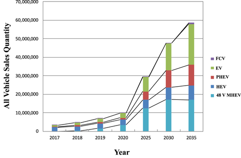
Fig. 2. (Color online) Market future trend: xEV sales quantity.2)
Download figure:
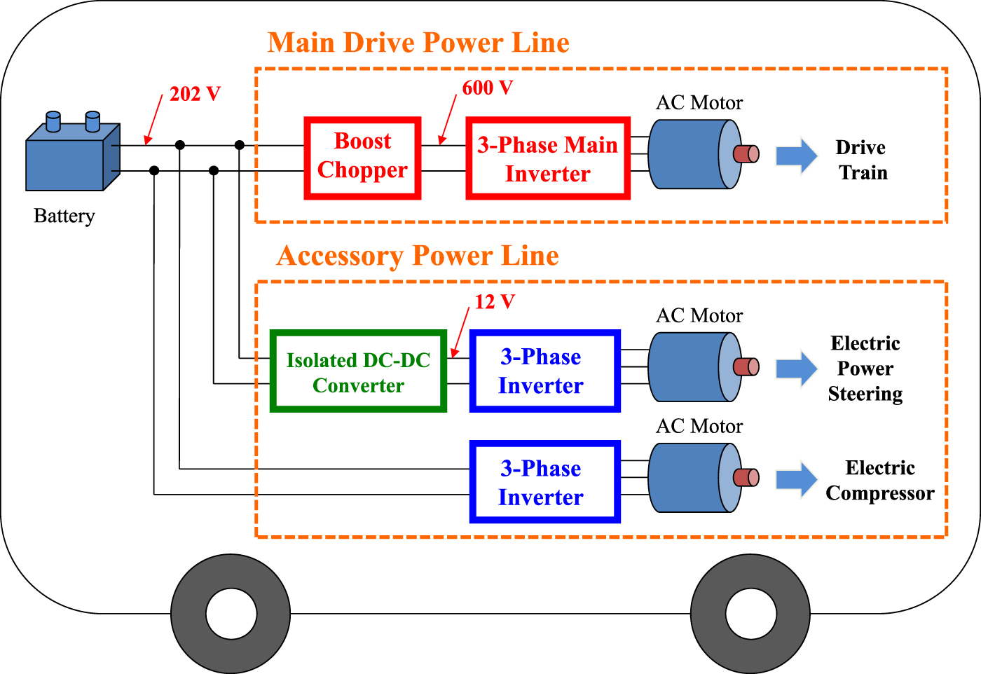
Standard image High-resolution imageHowever, automotive applications have many types of power electronics systems. For example, the power systems for HEVs have many power electronics systems as shown in Fig. 3. Furthermore, the requirement of each power electronics system is different from those of others as shown in Fig. 4. The vertices of the hexagon shown in Fig. 4 indicate the demand for power semiconductor devices in automotive applications in general. Regarding the main drive power line for HEVs as shown in Fig. 3, the output power is around 50–100 kW. In the case of accessory power lines, the output power needed for a three-phase inverter is about 1–7 kW. The efficiency of the main drive power line directly influences the fuel efficiency of the HEV. On the other hand, the demand for accessory power lines concerns both downsizing and low-cost performance.

Fig. 3. (Color online) Electric power train system for HEV.
Download figure:
Standard image High-resolution image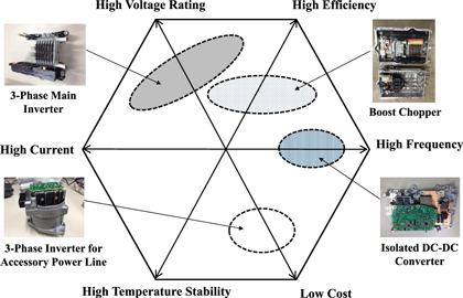
Fig. 4. (Color online) Performance requirement for each power electronics component in xEVs.
Download figure:
Standard image High-resolution imageOn the other hand, wide-bandgap semiconductor devices, such as gallium nitride (GaN) and silicon carbide (SiC) devices, have attracted great interest from the automotive application area,3–7) because SiC/GaN power semiconductor devices have much better performance than Si power devices from a lower intrinsic carrier concentration,4) a higher electric breakdown field,5) a higher thermal conductivity7–9) and a higher saturated electron drift velocity performance.4) Therefore, the electric drive train with SiC and GaN power semiconductor devices can improve their efficiency as compared with that of the usual Si IGBT devices. This means that HEVs using an electric drive train with SiC and GaN devices can achieve significantly improved fuel economy (a 3%–5% improvement in fuel efficiency in the case of SiC power semiconductor devices4)).
In the case of the main drive power line in Fig. 3, a SiC MOSFET is suitable for the boost chopper and three-phase main inverter because of its superior switching performance. Comparative switching waveforms between a SiC MOSFET (SCH2080KE) and a Si IGBT (GT40QR21) are shown in Fig. 5. From these figures, it is understood that a SiC power semiconductor device has low-loss performance in its switching transient. This means that the boost chopper can achieve miniaturized performance because higher switching frequency can be applied owing to its low-loss switching performance. In addition, when applying a SiC power semiconductor device in a three-phase inverter, its higher-efficiency performance can obtain higher fuel efficiency owing to its low-loss switching performance. The switching frequency of the conventional mass production automotive model is around 5–10 kHz in 2020; therefore a SiC MOSFET must aim at 50 kHz over the switching frequency in the future. As compared with that of GaN high electron mobility transistors (HEMTs), the switching frequency of SiC MOSFETs is limited because of the vertical structure of the power semiconductor device. Therefore, a SiC MOSFET is suitable only for 50–100 kHz high-power (50–400 kW) applications.
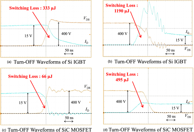
Fig. 5. (Color online) Comparative switching waveforms between Si IGBT and SiC MOSFET (Upper: 20 V div−1; Middle: 100 V div−1; Lower: 10 A div−1; Time: 100 ns div−1).
Download figure:
Standard image High-resolution imageOn the other hand, GaN power devices are suitable for isolated DC–DC converters because of their structure. In 2020, most GaN power semiconductor devices are GaN HEMTs, and they have superior performance in terms of high switching frequency because the gate input capacitance is lower than that in other types of power semiconductor devices.
To show the effectiveness of GaN HEMTs with high-switching characteristics, Fig. 6 indicates comparative efficiency data between a Si superjunction MOSFET (IPA60R125C6) and a GaN HEMT (TPH3208PS) in the case of a DC–DC converter (input voltage: 150 V; output voltage: 300 V; output power: 1 kW). From this figure, the DC–DC converter with a GaN HEMT can achieve higher efficiency as compared with that with a Si superjunction MOSFET in the case of 100 kHz over the switching frequency. In general, an isolated DC–DC converter is composed of huge magnetic components (a high-frequency transformer and a smoothing capacitor). Therefore, the high-frequency switching performance influences the miniaturized performance of the isolated DC–DC converter. In the automotive area, lightweight and miniaturized performance is the most important element. Therefore, it is clear that a GaN HEMT is suitable for an isolated DC–DC converter in automotive applications as shown in Fig. 3.
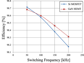
Fig. 6. (Color online) Comparative efficiency between Si MOSFET and GaN HEMT in the case of a DC–DC converter.
Download figure:
Standard image High-resolution imageHowever, wide-bandgap semiconductor devices are still too expensive to apply in the power electronics system in automotive applications. To solve this problem, lower voltage rating power semiconductor devices have been applied in the automotive area, particularly as shown in Fig. 7. However, the application of lower-power semiconductor devices requires additional technical demands such as adopting advanced compound semiconductor devices, adopting the soft-switching method and application of the series-connected method as shown in Fig. 7. These techniques can control or have high-stability performance for the surge voltage of each power semiconductor device in motor drive inverters for EVs and HEVs. In this paper, we will discuss each additional technical demand from the technical trend point of view.

Fig. 7. (Color online) Required low-cost technical trend in xEVs.
Download figure:
Standard image High-resolution image2. Impact of wide-bandgap semiconductor device applications on automotive area
In this section, we will discuss the application possibility of wide-bandgap semiconductor devices, such as GaN and SiC devices for automotive applications. The advantage of wide-bandgap semiconductor device application is the associated high-efficiency performance because of low on-resistance characteristics. From the system application side, the low-loss performance influences the high fuel efficiency directly. Furthermore, SiC power semiconductor devices can be applied in inverters for EVs, because EVs have high-voltage (over 800 V) lithium-ion batteries for their quick-charge requirement. An inverter using a SiC power semiconductor device operates effectively in the case of 1000 V DC bus-line applications.
Another advantage of wide-bandgap semiconductor devices is they can downsize power electronics systems.10) This is because passive components and cooling systems which occupy significant space in power converters can be downsized due to high-frequency operation and high-efficiency operation.
Generally, the loss of a power semiconductor device is divided into conduction loss and switching loss as shown in Fig. 8. Regarding wide-bandgap semiconductor devices, such as GaN and SiC devices, they can achieve low conduction loss and low switching loss performance as shown in Fig. 9. In particular, the switching loss influences high-frequency performance because the low switching loss characteristic allows shorter switching times. The high-frequency performance in the power electronics system can achieve miniaturized passive components such as miniaturized inductors and capacitors. For example, the effects of 10 times the switching frequency are shown in Figs. 10 and 11. In Fig. 11, the design conditions of each inductor show the same ripple value of each inductor current in the case of the same output power and the same frequency. And the power electronics system for HEVs is mainly composed of passive components such as an inductor, a transformer, and a smoothing capacitor. Each passive component determines the volume of the power electronics system for HEVs. This means that SiC/GaN power semiconductor devices are suitable for isolated DC–DC converters as shown in Fig. 3. Because of their miniaturized performance requirement, there are many advantages to applications of SiC/GaN power semiconductor devices in the automotive area. However, the xEV market will be a hotspot in the next decade. Therefore, the real requirement for the power electronics system of xEVs is lower cost.
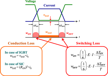
Fig. 8. (Color online) Loss in power devices.
Download figure:
Standard image High-resolution image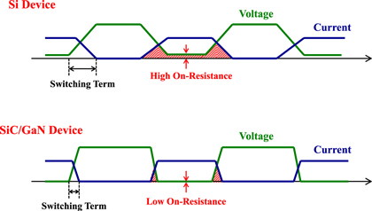
Fig. 9. (Color online) Schematic diagram of switching waveforms.
Download figure:
Standard image High-resolution image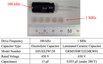
Fig. 10. (Color online) Comparative capacitor volume for each frequency.
Download figure:
Standard image High-resolution image
Fig. 11. (Color online) Comparative inductor volume for each frequency.
Download figure:
Standard image High-resolution imageFor this requirement, the series-connected method and soft-switching method are an effective solution in the automotive area as shown in Fig. 7. In the next section, we will discuss the feasibility of the soft-switching method.
3. Soft-switching technique for automotive applications
3.1. What is soft switching?
Wide-bandgap semiconductor devices (SiC/GaN) are suitable for automotive applications because their characteristics of a high switching transient and high switching speed can achieve the high-frequency switching discussed in section 2. However, the high switching transient induces a huge surge voltage in wide-bandgap semiconductor devices. The effective solution is to adopt soft-switching techniques in power electronics systems using wide-bandgap semiconductor devices. The soft-switching technique can achieve low surge voltage and low switching loss performance in power electronics systems. Specifically, the soft-switching technique requires additional soft-switching circuits including resonant inductors, resonant capacitors, and active switches. Furthermore, a soft-switching circuit operates only on switching transient timing, with a turn-on or turn-off transient. In switching transient timing, the voltage and current transient across the active power semiconductor device will be controlled softly by using an LC resonant phenomenon actively. Schematic diagrams of the voltage and current waveforms in the case of conventional hard-switching and soft-switching schemes are shown in Fig. 12. There is no surge voltage or switching loss in the soft-switching scheme. Experimental comparative data are also shown in Figs. 13 and 14. In the case of soft switching, the surge voltage is controlled effectively using an LC resonant phenomenon. This means that a lower-cost power semiconductor device can be applied in power electronics systems in automotive applications using soft-switching techniques.

Fig. 12. Schematic diagram of each switching waveform.
Download figure:
Standard image High-resolution image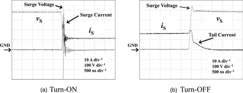
Fig. 13. Hard-switching waveforms.
Download figure:
Standard image High-resolution image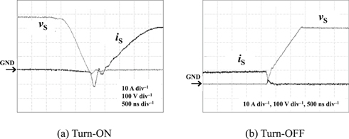
Fig. 14. Soft-switching waveforms.
Download figure:
Standard image High-resolution imageThe soft-switching transient has three types of modes:
- 1)Zero-voltage switching (ZVS)
- 2)Zero-current switching (ZCS)
- 3)Zero-voltage and zero-current switching (ZV&ZCS)
When the active switching device is turned on when the DC bus-line voltage is zero, the transient operation is called ZVS. On the other hand, when the active switching device is turned on when current through the device is zero, the transient is called ZCS. ZV&ZCS is a hybrid transient operation of ZVS and ZCS.
The soft-switching technique is excellent with wide-bandgap semiconductor devices. The disadvantage of wide-bandgap semiconductor devices is their surge voltage due to a high-speed switching transient. On the other hand, the switching transient is mild in the case of the soft-switching scheme. Therefore, researchers and scientists can concentrate on the on-resistance discussion for power semiconductor device development.
3.2. Soft-switching technique for three-phase inverter
For automotive applications, the most important power electronics system is the three-phase inverter for motor drive applications. To achieve soft-switching operation in a three-phase inverter, there are three circuit topologies that can be used as shown in Fig. 15. Each circuit topology has an additional soft-switching circuit with a resonant inductor, a resonant capacitor and an active power semiconductor device for achieving soft-switching operation. The DC link method has a simple and lower-cost performance, whereas a soft-switching circuit requires an active power semiconductor device in a DC bus-line for dividing the DC voltage source side and load side. Therefore, the DC link method cannot achieve high efficiency because of the huge loss in series-connected power devices. Similarly, the AC link method can achieve high-efficiency performance, but the switching operation is limited for obtaining complete soft-switching operation. In the AC link method, the total harmonic distortion value is higher than those of soft-switching methods. This means that motor-side noise increases in the AC link method. The auxiliary resonant commutated pole (ARCP) method is complicated in terms of circuit structure, but this method can achieve high-efficiency and low-noise performance. Therefore, the ARCP will be adopted and evaluated in this paper.

Fig. 15. Three types of soft-switching methods for three-phase inverter.
Download figure:
Standard image High-resolution imageThe circuit configuration of a half-bridge ARCP inverter is illustrated in Fig. 16. In this study, not only the main switches S1 and S2 but also the auxiliary switches Sa1 and Sa2 are a SiC MOSFET and SiC SBD package.11) In the figure, Lf is the output filter and Ro is the output load. The operation principle of the ARCP soft-switching inverter is explained by using the case of a half-bridge inverter as shown in Fig. 16. In general, a bridge-type inverter has four switching patterns as shown in Fig. 17. And two switching patterns transit alternately for the phase current direction (between State A and State B, or between State C and State D). In each switching pattern transition, the ARCP circuit operates in soft switching in all power semiconductor devices. The main switch can achieve a zero-voltage turn-off and zero-voltage and zero-current hybrid turn-on transition using the LC resonant phenomenon between the auxiliary inductor Lr and the resonant capacitors Cr1 and Cr2 as shown in Fig. 18. Furthermore, the auxiliary switch achieves zero-current turn-on and zero-current turn-off.
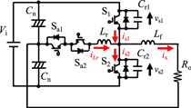
Fig. 16. (Color online) Equivalent circuit of ARCP inverter.
Download figure:
Standard image High-resolution image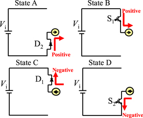
Fig. 17. (Color online) Four switching patterns of inverter.
Download figure:
Standard image High-resolution image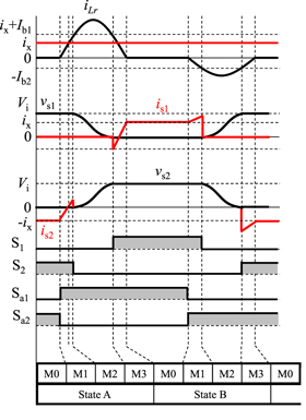
Fig. 18. (Color online) Operation principle of ARCP inverter (in the case of a positive one).
Download figure:
Standard image High-resolution image3.3. Experimental discussion of three-phase inverter in ARCP method
The experimental conditions are as follows: the input voltage Vi is 200 V, the switching frequency is 5 kHz, the output power rating is 2 kW, the auxiliary inductance Lr is 25 μH, and the resonant capacitances Cr1 and Cr2 are 0.1 μF. SiC MOSFETs are applied for all power semiconductor devices in this ARCP inverter. The experimental waveforms of main switch S2 are indicated in Fig. 19. In the turn-off transition, it is clear that ZVS is achieved from Fig. 19(a). And in the turn-on transition, ZV&ZCS is achieved perfectly as seen in Fig. 19(b). The switching loss is theoretically equal to zero in the ZVS transition. However, the switching loss exists in the ZVS turn-off transition actually because the IGBT has its tail current in the turn-off transition. On the other hand, when a tail current exists in the case of the SiC MOSFET, a full SiC soft-switching inverter has a very low switching loss.11) Therefore, a SiC MOSFET is suitable for the soft-switching method for automotive applications.
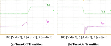
Fig. 19. (Color online) Experimental switching waveforms in the case of ARCP method.
Download figure:
Standard image High-resolution imageWide-bandgap semiconductor devices (SiC/GaN) have technical difficulties in the case of power converter applications because of their lower gate threshold voltage.12) The difficulty is a false turn-on phenomenon in bridge-type power converters. Short-circuit accidents will be caused by this phenomenon. The false turn-on phenomenon arises from recovery current in antiparallel diodes. In the case of the soft-switching method, the turn-off operation transits softly. Therefore, the recovery current is controlled effectively in the soft-switching method. This means that the false turn-on phenomenon is prevented in the soft-switching method. Comparative gate voltage waveforms are shown in Fig. 20. It can be seen from this figure that the soft-switching method can control the false turn-on phenomenon effectively. This again confirms that a SiC MOSFET is suitable for the soft-switching method for automotive applications.
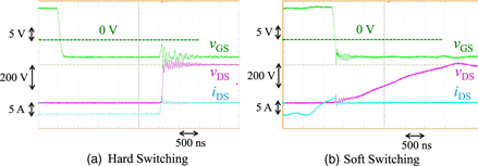
Fig. 20. (Color online) Comparative gate voltage waveforms.
Download figure:
Standard image High-resolution image3.4. Soft-switching technique for isolated DC–DC converter
In the case of an isolated DC–DC converter, this application requires lower cost and miniaturized performance. In response to the demand, some auto manufacturers apply soft-switching techniques to an isolated DC–DC converter. In recent years, LLC converters have been selected for automotive applications for isolated DC–DC converters linked between a high-voltage battery and a 12 V auxiliary battery. The equivalent circuit of an LLC converter is illustrated in Fig. 21. Using the resonant phenomenon between a resonant inductor and a resonant capacitor, complete soft-switching operation has been achieved.
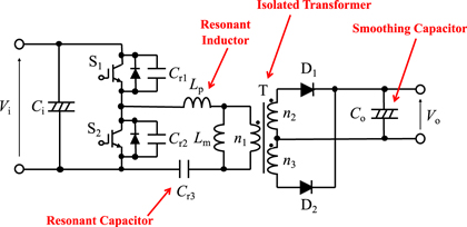
Fig. 21. (Color online) Equivalent circuit of LLC converter.
Download figure:
Standard image High-resolution imageFigure 22 shows the experimental voltage and current waveforms of power semiconductor devices in an LLC converter. In the turn-off transition, ZVS is achieved from Fig. 21. And in the turn-on transition, ZV&ZCS is achieved perfectly from this experimental result.

Fig. 22. (Color online) Experimental waveforms of LLC converter.
Download figure:
Standard image High-resolution image4. Series-connected power semiconductor device method
In response to the lower-cost demand, power semiconductor devices with lower voltage rating applications have been employed and shown to be effective in the automotive area. For the application, the series-connected power semiconductor device method is one of the solutions.
The series-connected active power semiconductor device method using low voltage rating power semiconductor devices of power conversion systems has been improved from the cost and low-loss performance points of view.13) Figure 23 shows the results with 10 × 60 V, 6 × 100 V, and 4 × 150 V MOSFETs replacing a single 600 V Si device and a single 650 V SiC device. In the series-connected active power semiconductor device method, two or more semiconductor switches are controlled as a single switch. Clearly, the series connection method shows a lower total on-resistance than a single 600 V Si device or a 650 V SiC device. Figure 23 only considers conduction losses, but depending on the application, the performance of parasitic elements and body diodes can affect the losses. Typically, low-voltage MOSFETs have good recovery characteristics for their body diodes and good switching performance.14) Therefore, the difference from a single high-voltage MOSFET can be even greater. Furthermore, since multiple devices are used, the total thermal resistance can be reduced and the heat sink can be much smaller.15)

Fig. 23. (Color online) Relationship between breakdown voltage and total on-resistance.
Download figure:
Standard image High-resolution imageHowever, the voltage imbalance phenomenon occurs in the series-connected active power semiconductor device method in the case of not only hard-switching power conversion systems but also soft-switching ones.16,17) LLC converters are soft-switching converters, and conduction loss accounts for the majority of the loss.18–20) Therefore, LLC converters have good compatibility with series-connected methods that can reduce the total on-resistance. In this paper, the voltage imbalance mechanism in each power semiconductor device is analyzed and the cause of the voltage imbalance phenomenon in the series-connected method is extracted in a boost chopper for EV motor drive applications. Furthermore, the voltage imbalance phenomenon in the series-connected method in the case of a soft-switching DC–DC converter is evaluated using an experimental setup and a novel control method for voltage imbalance in each power semiconductor device in the case of a soft-switching DC–DC converter.
5. Analysis of series-connected power semiconductor device method in hard switching
5.1. Configuration of the analysis circuit
Figure 24 shows the boost chopper circuit selected for this analysis.  is a voltage balance capacitor. The circuit configuration is very similar to a multi-level topology, but
  is composed of very small capacitances unlike a flying capacitor.13,21,22) The purpose of
  is to stabilize voltage levels during switching transients. In the case of two series connections, if all MOSFETs in each arm synchronously turn on and turn off, the voltage of
  is in balance at half the input voltage. In reality, there is a slight time difference between the MOSFETs' switching timings; therefore voltage imbalance occurs. In particular, the voltage imbalance phenomenon is caused by the difference in turn-off timing.
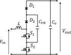
Fig. 24. Boost chopper circuit.
Download figure:
Standard image High-resolution image5.2. Voltage imbalance phenomenon
Voltage imbalance is proportional to the difference in turn-off timing.23) Figure 25 shows a simplified diagram of the transition of the drain–source voltage when  and
and  are turned off.
  is the voltage between the drain and source of
  and
and  is that of
 is the difference between
  and
and  These satisfy the conditions given by


 is the delay time of the turn-off start timing and
  is the time until the delayed turn-off ends. And r1 and r2 denote the voltage transient value dv/dt of each power semiconductor device. When the voltage transitions of
  and
and  are approximated linearly with
  and
and  respectively,
  and
and  are as follows:


Employing Eqs. (1)–(4), one can calculate Eqs. (5) and (6):


Eliminate  from Eqs. (3) and (4), and voltage imbalance is given by Eq. (7):

From Eq. (7), the voltage imbalance increases in proportion to the turn-off delay. Even though the turn-off timing is synchronized, voltage imbalance will occur when  and
and  are different.
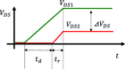
Fig. 25. (Color online) Turn-off switching waveforms.
Download figure:
Standard image High-resolution imageThere are multiple causes of delays in turn-off timing, such as errors in parasitic elements and errors in device characteristics.24) The influence from each parameter of the power semiconductor device in the series-connected method is analyzed in conditions of a 500 W boost chopper (input voltage Vi = 100 V, output voltage Vo = 200 V, switching frequency fs = 50 kHz). Each parameter of the power semiconductor device is defined as illustrated in Fig. 26. The result is indicated in Fig. 27. From this result, the error in threshold voltage of a power semiconductor device has great influence on the voltage imbalance phenomenon in the series-connected method.
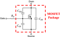
Fig. 26. (Color online) Each parameter of power device.
Download figure:
Standard image High-resolution image
Fig. 27. (Color online) Analyzed result.
Download figure:
Standard image High-resolution imageEquation (7) means that the voltage imbalance becomes smaller as  becomes smaller. In this case, a small
  is the same as a slow voltage transition between the drain and source. However, reducing the voltage increase rate in hard-switching applications sacrifices converter efficiency and/or size. Therefore, for hard-switching applications, a gradual voltage transition is not practical as a method to suppress voltage imbalance. Several methods have been discussed as voltage imbalance suppression methods.25–34) In Refs. 31–33, a voltage balancing method using digital control has been proposed. Voltage balance is achieved by controlling the turn-off timing. However, this method requires a high-speed microcomputer or an external delay line IC. These components can lead to increased power conversion system costs. In Ref. 34, voltage balancing is performed by actively controlling dv/dt and an additional circuit on the gate driver. In any case, for hard-switching applications, the cost is increased or control becomes complicated.
6. Analysis of series-connected power semiconductor device method in soft switching
The evaluation target of a soft-switching DC–DC converter is shown in Fig. 28. An LLC converter is selected for the evaluation for the control of each voltage across the power semiconductor devices.  and
and  are the voltage balance capacitors. In the LLC converter, turn-on operation is performed as ZVS, and there is no influence from the delay of turn-on timing. In turn-off, soft switching is achieved by charging the parasitic capacitance with the excitation current during dead time.35,36) Therefore, the drain–source voltage transition at turn-off is slow. From Eq. (7), LLC converters can suppress voltage imbalance without increasing switching loss compared with hard-switching applications. Furthermore, the drain–source voltage increase rate dv/dt depends on the excitation current; designing a large transformer excitation inductance to reduce conduction loss is also effective in suppressing voltage imbalance. In summary, a greater voltage imbalance suppression effect can be obtained by designing a large excitation inductance.
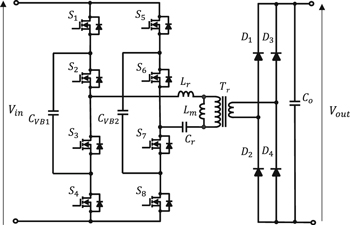
Fig. 28. Series-connected method LLC converter.
Download figure:
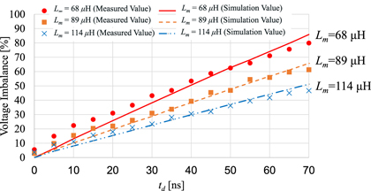
Standard image High-resolution imageThe simulation tool PLECS and an experimental circuit (120 W LLC converter input voltage Vin = 40 V, output voltage Vo = 19 V, switching frequency fs = 84 kHz) are used to investigate the proposed method. Three transformers with different excitation inductances  are used to obtain different excitation currents. In this experiment, the
  gate signal is intentionally delayed by 0–70 ns from the
  gate signal.
Figure 28 shows the simulation and experimental results. The dots show the experimental results and the solid line shows the simulation results. It is clear that the parameter design of the soft-switching converter can control the voltage balance performance from the evaluation result. Voltage imbalance is defined by

There is a difference between the experimental and simulation results at a short td. This is because the simulation does not take into account device variations. The experimental results show a slight voltage imbalance even with a turn-off delay of 0 ns. This is consistent with the intercept term in Eq. (7) and can be assumed to be voltage imbalance due to device characteristic differences.
Figure 29 indicates that the design of passive component parameters in a power electronics circuit can control the voltage balance of each series-connected power semiconductor device in the case of the soft-switching method. Therefore, it is clear that the series-connected method is suitable for the soft-switching method from the power electronics system point of view.
Fig. 29. (Color online) Evaluated result.
Download figure:
Standard image High-resolution image
7. Conclusions
In the automotive application area, high fuel efficiency performance will be required by strict EU regulation of exhaust gas. One of the solutions is the application of wide-bandgap semiconductor devices, such as GaN and SiC devices, in main drive power lines and accessory power lines in next-generation automotive applications. However, the lower-cost demands have increased in the automotive application area in recent years.
In this paper, the soft-switching method and the series-connected method are proposed to solve the problem. The series-connected method can achieve low-cost and high-efficiency performance. High-efficiency performance is limited because of switching losses due to the parasitic output capacitance in GaN/SiC power semiconductor devices. The soft-switching method can achieve higher-efficiency performance as compared with the conventional switching method in the case of GaN/SiC power semiconductor device applications. Furthermore, in response to lower-cost demands, the combination of the series-connected method and the soft-switching method is effective and a better solution from the cost and power electronics stability points of view. This stability means voltage balance performance.
Applications of wide-bandgap power semiconductor devices are faced with some technical hurdles; however, using the proposed combination technique with the soft-switching method and series-connected method, we can confirm some possibilities for automotive applications.