


Abstract
The CZO films annealed at 500°C are smoother and they have the maximum value of electron-phonon interaction. The CZO films annealed at 500°C have the maximum value of optical density. The absorption edge of films up to 500°C has a redshift and over 500°C they have a blue shift. The CZO films annealed at 500°C have the minimum value of band-to-band transitions energy. The as-deposited CZO films are more disordered. The empirical optical mathematical equation from linear fitting for these films was given as  . It was demonstrated that values of the steepness parameters of CZO films are represented by a decreasing function while electron-phonon interactions by an increasing function with increasing annealing temperature. This may be ascribed to a change in iconicity and action valences of CZO films. Considering
  ,
,  , and
, and  for ZnO, the coordination number constants
  were calculated and for CZO films annealed at 600°C, β has a minimum value about of 0.18. Swanepoel method parameters also were obtained.
Export citation and abstract BibTeX RIS
Introduction
Over the last few decades, dielectric-electric properties as a function of frequency and temperature have been comprehensively studied [1]. Zinc oxide belongs to group II-VI composite semiconductor and is known as an n-type semiconductor on account of the insufficiency of oxygen. ZnO has 60 meV excitation binding energy and a large direct band-gap of approximately 3.4 eV. ZnO is very suitable for gas sensor applications since its surface is so sensitive to oxygen and hydrogen and has a high thermal conductivity [2]. According to reported works, there could be several reasons for the development of RT ferromagnetism in TM-doped ZnO such as uncontrollable ferromagnetic clusters, secondary phases, and defects. It has been also reported that Co is highly soluble in ZnO, and Co-doped ZnO can have ferromagnetic or non-ferromagnetic properties at RT, depending on its growth technique and conditions. Moreover, using different additional doping elements, such as Al, Cu, and Ga in TM-doped ZnO can result in RT ferromagnetism and/or enhanced ferromagnetism, which is known as carrier-induced RT ferromagnetism [3]. Deposition of ZnO can be accomplished with techniques such as molecular beam epitaxy, metal-organic chemical vapor deposition, pulsed laser deposition, radio-frequency magnetron sputtering, and spray pyrolysis deposition that has been used to deposit ZnO on different substrates [4]. The aim of the present work is also to discuss the correlation between these parameters and temperature.
Experimental details
Details of the deposition processing of films are given in our previous report [5].
Results and discussion
In our previous work, PL and EDX have been studied and the difference between photoluminescence emission peaks of ZnO films compared with copper-doped ZnO films is mainly due to a green emission at a position of about 530 nm which was related to the transition from donor levels to the valence band because of oxygen ions vacancies and the replacement of Cu atoms ions instead of Zn atoms in the ZnO structure. The percentages of copper and zinc atoms in as-deposited copper-doped ZnO films were 4.31 and 23.48%, respectively [5]. It is observed that the nano- and micro-roughness is created by fluctuations in the surface of short wavelengths, characterized by hills (local maxima) and valleys (local minima) of varying amplitudes and spacing. The root mean square (RMS) of CZO film for room temperature, 400, 500, and 600°C was 5.74, 4.70, 6.02, and 10.1 nm, respectively (these results are reported in table 1). According to AFM images and particle distribution (see fig. 1), surface morphology changes can be analyzed by changes in annealing temperature in the zinc oxide layers in such a way that in the unbacked and annealed layer, the particle shape is almost identical and with the same distributions. Also, the surface roughness of the layers changed in the range of 4 to 10 nm with annealing, and the lowest surface roughness is related to the annealed layer at 400°C. The CZO substrate at 600°C has a relatively large root mean square. In our previous work, XPS and XRD have been studied. In these patterns, only a well-defined diffraction peak is observed at around 34°, which is ascribed to the crystalline (002) planes of the ZnO phase. In the spectrum (XPS) of CZO film, broadbands at around 932.5 eV, 943 eV and 952 eV were observed, which correspond to the Cu  peak of Cu1+, the Cu
  of Cu2+ and the Cu
  , respectively [6,7].
Table 1:. The values of the direct band-gap energy (Eg
), the band tail width (EU), steepness parameter  , and electron-phonon interaction (
 ) and RMS of the samples.
| Sample | Wavelength of | En | Eg | The constant | Steepness | ( ) ) | RMS |
|---|---|---|---|---|---|---|---|
| absorption | (eV) | (eV) | ( ) ) | parameter 
| (eV) | (nm) | |
| edge (nm) |

| (eV) | |||||
| CZO (as-deposited) | 364.514 | 0.515 | 3.21 | 35.88 | 20E−10 | 3.33E10+8 | 7.238 |
| CZO (400°C) | 386.736 | 0.388 | 3.18 | 34.52 | 6.69E−10 | 9.96E10+8 | 7.999 |
| CZO (500°C) | 398.484 | 0.168 | 3.17 | 26.10 | 2.52E−10 | 26.43E10+8 | 7.056 |
| CZO (600°C) | 389.245 | 0.310 | 3.19 | 32.18 | 4.12E−10 | 16.16E10+8 | 7.817 |

Fig. 1: 3-D AFM images ( ) of CZO (a) as-deposited, (b) 400°C, (c) 500°C, and (d) 600°C.
Download figure:
Standard imageFor each of these four samples, we measured the transmission and reflection spectrum at room temperature, and 400, 500, and 600°C to calculate the absorption coefficient from the ( ) ratio, spectral dependence of the index of refraction. With the increase of energy from 3 to 3.2 eV, the optical absorption coefficient (see fig. 2) of the oxide layer has also increased sharply, because in this energy range the frequency of the electromagnetic wave is close to or equal to the frequency of the resonant electrons in the copper oxide molecules. Also, with the annealing of the layers and the increase of the annealing temperature, a shift of the absorption edge towards larger photon energy is observed. The shift in absorption edge might have resulted from the formation of the conjugated bond system caused by bond cleavage and reconstruction. The plots indicate that for all the samples, the optical density increased almost linearly with increasing photon energy up to the absorption edge after which a sharp rise in optical energy was noticed. The variation of the optical density with varying post-deposition annealing temperatures can also be linked in terms to the stoichiometric changes induced by copper vacancies and neutral spaces. The formation of these defects depends on the sticking coefficient, nucleation rates, and the movement of intruding zinc and copper ions during deposition which is a function of the concentration of the reacting species [8].
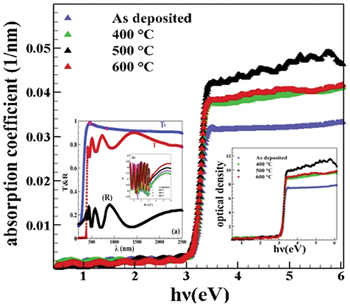
Fig. 2: Variations of the optical absorption coefficient  vs. energy photon (hν). Inset: optical density (Dopt
) and R and T and n for the samples.
vs. energy photon (hν). Inset: optical density (Dopt
) and R and T and n for the samples.
Download figure:
Standard imageThe skin depth  is a measure of the distance that an optical beam penetrates in glass samples before the beam is scattered. It is related to the absorption coefficient,
  , according to the following simple relationship [9]:

where k is the extinction coefficient of films. Figure 3 shows the variation of skin depth as a function of photon energy for all films. It is clear from the figure that the skin depth increases as the wavelength increases; this behavior could be seen in all samples. It is seen from fig. 3 that the skin depth changes from  to
to  with temperature. The value of the cut-off energy,
  , of the films was about 3.20 eV and the value of the
  was about 387 nm. The highest skin depth is found for the CZO films annealed at 500 and 600°C which indicates the effect of temperature. The complex dielectric constant,
  , of semiconducting thin films is based on the real,
  , and imaginary,
  , parts of the optical dielectric constant and can be characterized by the following relation [10]:


The spectra of real and imaginary parts of the optical dielectric constant are shown in fig. 3. The variation of  behaves with the same trend as n, while following the behavior of k with photon energy [11]. The optical band-gap is obtained from the intersection of the real and imaginary parts vs. photon energy. This observed trend may also be correlated with the distribution defects of atoms. The magnitude of the optical energy band-gap values differs within the range of 3.17 eV and 3.21 eV.

Fig. 3: The variations of the skin depth  . Inset: dependences of the real and imaginary parts of the complex dielectric vs. photon energy (
 ) for the samples.
Download figure:
Standard imageThe tail of the absorption edge is exponential, indicating the presence of localized states in the energy band-gap. The amount of tailing can be predicted to a first approximation by plotting the absorption edge data in terms of an equation originally given by Urbach [12]. The absorption edge gives a measure of the energy band-gap and the exponential dependence of the absorption coefficient, in the exponential edge region the Urbach rule is expressed as [13,14]

where  is a material constant of films. The parameter hν corresponds to the energy of the lowest free excited state at zero lattice temperature, while Eu
is the Urbach energy, which characterizes the slope of the exponential edge. This parameter determines the steepness of the Urbach tail. Urbach energy values change inversely with the optical band-gap (see fig. 4). The Urbach energy values of the films increase with a decrease in doping temperature. The decrease of Urbach energy suggests that the atomic structural disorder of doped films is decreased by increasing the doping temperature. This behavior can result from increasing the grain size. The size of the grains varies with the doping and influences the value of the optical energy gap; this increased crystallinity leads to a redistribution of states from band to tail and may be attributed to the improvement. As a result, both a decrease in the optical gap and expansion of the Urbach tail take place. The optical gap is reduced with increasing temperature. It is worth bearing in mind that the Urbach tail energy is closely related to the disorder in the film network. Since the ion radius of Cu is larger than ZnO, the Cu introduction into the films is then followed by the lattice distortion and consequently disorder creation which causes the optical reduction. Therefore, as the band-gap decreases, the magnitude of defect energy increases. This supports our argument that sub-band states formed in between the valence and conduction bands result in the narrowing of the band-gap. With increasing temperature, the number of defect levels below the conduction band increases to such an extent that the band edge is shifted deep into the forbidden gap, thereby reducing the effective band-gap of CZO. The empirical equation from this linear fitting is given as [15]
is a material constant of films. The parameter hν corresponds to the energy of the lowest free excited state at zero lattice temperature, while Eu
is the Urbach energy, which characterizes the slope of the exponential edge. This parameter determines the steepness of the Urbach tail. Urbach energy values change inversely with the optical band-gap (see fig. 4). The Urbach energy values of the films increase with a decrease in doping temperature. The decrease of Urbach energy suggests that the atomic structural disorder of doped films is decreased by increasing the doping temperature. This behavior can result from increasing the grain size. The size of the grains varies with the doping and influences the value of the optical energy gap; this increased crystallinity leads to a redistribution of states from band to tail and may be attributed to the improvement. As a result, both a decrease in the optical gap and expansion of the Urbach tail take place. The optical gap is reduced with increasing temperature. It is worth bearing in mind that the Urbach tail energy is closely related to the disorder in the film network. Since the ion radius of Cu is larger than ZnO, the Cu introduction into the films is then followed by the lattice distortion and consequently disorder creation which causes the optical reduction. Therefore, as the band-gap decreases, the magnitude of defect energy increases. This supports our argument that sub-band states formed in between the valence and conduction bands result in the narrowing of the band-gap. With increasing temperature, the number of defect levels below the conduction band increases to such an extent that the band edge is shifted deep into the forbidden gap, thereby reducing the effective band-gap of CZO. The empirical equation from this linear fitting is given as [15]

The increase in Urbach energy confirms the increase in the width of localized states in the band-gap and hence is responsible for band-gap decay of CZO thin films with increasing temperature. The steepness parameter, which demonstrates the broadening of the absorption band, can be determined empirically using the following equation [16]:

where the steepness parameter is the Boltzmann constant and T is the absolute temperature. Furthermore, the steepness parameter also determines the strength of electron-phonon interaction ( ) and both are related to each other via the following relationship [17]:

It is demonstrated that the values of the steepness parameter are decreasing while electron-phonon interaction is increasing with the substitution of CZO thin films. This may be ascribed to the change in iconicity and caution valence of CZO thin films.
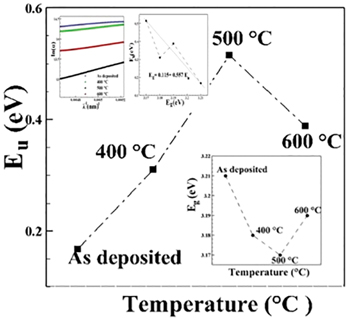
Fig. 4: Dependency of doping on the optical energy gap and the band tail width, relation between the energy band-gap and the width of the Urbach tail. Inset: dependence of  upon the
  for the samples.
Download figure:
Standard imageThe optical conductivity  of films was calculated using the relation [18]

where c is the velocity of the incident light. It can be seen that the optical conductivity for thin films increases with the increase of photon energy; this increase is due to the high absorbance of the films in that region (see fig. 5). This suggests that the increase in optical conductivity is due to electrons excited by photon energy. The origin of this increase may be attributed to some changes in the structure of the film due to the doping and the value of temperature.
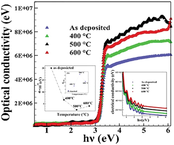
Fig. 5: The variations of optical and electrical conductivity vs. photon energy. Inset: the steepness parameter and the electron-phonon interaction with the doping and temperature for the samples.
Download figure:
Standard imageDecrease in extinction coefficient implies that these sudden intense peaks indicate the region of deeper penetration for electromagnetic waves and these show the high optical conductivity.
The electrical conductivity  in terms of wavelength
  and optical conductivity
  of films can be calculated using the formula [19]

The electrical conductivity of the crystal is decreased gradually as the photon energy increases. The decrease in electrical conductivity is due to the high absorbance of thin films and may be due to electron excitation by the photon [20].
Plotting  vs.
vs.  allows us to determine the oscillator parameters. The refractive index
  of films in infinite wavelength can be determined by the following relation [21]:

where Ed
and Eo
are single-oscillator constants, Eo
is the energy of the effective dispersion oscillator, and Ed
the so-called dispersion energy, which measures the intensity of the inter-band optical transitions. Experimental verification of relation (11) can be obtained by plotting  vs.
vs.
 , as illustrated in fig. 6, which yields a straight line for normal behavior having the slope
  , and the intercept with the vertical axis equal to
  . According to the single-oscillator model, the single-oscillator parameters Eo
and Ed
are related to the imaginary part of the complex dielectric constant. The dispersion energy Ed
obeys the following empirical relationship [22]:
. According to the single-oscillator model, the single-oscillator parameters Eo
and Ed
are related to the imaginary part of the complex dielectric constant. The dispersion energy Ed
obeys the following empirical relationship [22]:

where Nc
is the coordination number of the caution nearest neighbor to the anion, Za
is the formal chemical valiancy of the anion, Ne
is the effective number of valence electrons per anion and β is a constant (0.37±0.04) for covalently bonded crystalline and amorphous chalcogenides and  eV for halides and most oxides that have ionic structure). Taking
  ,
,  ,
,  for ZnO [22], the β values for the different ZnO nanocrystalline films were determined and are given in table 2. As observed, the obtained values of β for films are in agreement with that published for CZO [22]. The crude refractive index (ncrud
) of the as-prepared and annealed films under investigation can be computed based on the envelope method via transmission spectrum proposed using the Swanepoel method [23]. The values of n can be computed at any wavelength via the relation
for ZnO [22], the β values for the different ZnO nanocrystalline films were determined and are given in table 2. As observed, the obtained values of β for films are in agreement with that published for CZO [22]. The crude refractive index (ncrud
) of the as-prepared and annealed films under investigation can be computed based on the envelope method via transmission spectrum proposed using the Swanepoel method [23]. The values of n can be computed at any wavelength via the relation
where

This states that refractive index n can be determined only from the values of Tm and TM obtained from experimental envelope generation.

Fig. 6: The variation of  vs.
vs.
 and the variation of both the Eo
and Ed
with the temperature for the samples.
and the variation of both the Eo
and Ed
with the temperature for the samples.
Download figure:
Standard imageTable 2:. The empirical equation from linear fitting  of samples upon the
  and the single-oscillator energy and dispersion energy parameters, constant.
| Sample | Line equation | Eo | Ed | β |
|---|---|---|---|---|
| (eV) | (eV) | |||
| CZO |
| 8.59 | 18.00 | 0.28 |
| (as-deposited) | ||||
| CZO (400°C) |
| 5.79 | 13.17 | 0.21 |
| CZO (500°C) |
| 6.08 | 12.42 | 0.19 |
| CZO (600°C) |
| 5.89 | 11.33 | 0.18 |
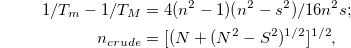
TM and Tm are the transmission maximum and the corresponding minimum at a certain wavelength. The transmittance of the substrate in the absence of film Ts gives an interference-free spectrum [23],

The transmittance and reflectance spectrum of thin films at different temperatures together with the transmittance of the uncoated glass substrate is shown in fig. 1. Values of ncrud
at any adjacent maximal (or minimal), that have been computed by eq. (13), are used to deduce crude thickness thin films,  . If ne1 and ne2 are the refractive indices of two adjacent maxima or minima at wavelengths
  and
and  , then the crude thickness of the films is expressed as [24]

The values of film thickness are listed in table 3 (d1), where nm
and  are the refractive indices at two adjacent maxima (or minima) and
  and
and  are the corresponding wavelengths. To improve the accuracy of thickness films there is a set of the order number mo
for the interference fringes which are deduced via the relation [24]
are the corresponding wavelengths. To improve the accuracy of thickness films there is a set of the order number mo
for the interference fringes which are deduced via the relation [24]

The order number m can increase precision, by rounding it to an integer, if n and λ were taken at maxima, or half-integer if n and λ were taken at minima. We would denote an improved order number after rounding as mnew
. The thickness dcrude
can be improved with improved mnew
at each extreme  , by rearranging eq. (16) in terms of d,

We would denote an improved thickness as dnew
. After obtaining the thicknesses of all the films at all extremes, the new thickness should be averaged,  . In previous reports [24], the transmittance and reflectance spectrum for samples were shown. Next, by taking the approximate value of mo
, a new order number m is produced, where
. In previous reports [24], the transmittance and reflectance spectrum for samples were shown. Next, by taking the approximate value of mo
, a new order number m is produced, where  , at the maximum points in the optical transmission spectrum and
  , at minimum points in the optical transmission spectrum. The final values of the new refractive index n2 and other mentioned values are listed in table 3. Then, to compute the standard deviation values
  and deviation ratio pi
about the actual value for each of d1 and d2, we use the following relation [24]:
and deviation ratio pi
about the actual value for each of d1 and d2, we use the following relation [24]:
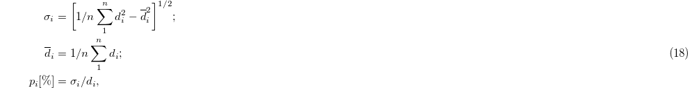
where i is a number equal to 1 or 2 and n refers to the number of thicknesses.
Table 3:. Two values of envelopes TM and Tm of the samples and the computed values of refractive index and film thicknesses are based on the envelope method.
| Sample (no) | λ (nm) | TM | Tm | Ts | S | n1 | n2 | d1 (nm) | m0 | m | d2 (nm) | n |
|---|---|---|---|---|---|---|---|---|---|---|---|---|
| CZO (as-deposited) | ||||||||||||

| 496.03 | 0.67 | 0.57 | 0.90 | 1.44 | 2.60 | 2.57 | 398.19 | 4.17 | 6.94 | 662.32 | 2.34 |

| 580.37 | 0.69 | 0.59 | 0.88 | 1.50 | 2.01 | 2.01 | 595.44 | 4.12 | 3.49 | 504.32 | 2.06 |
| 714.23 | 0.70 | 0.61 | 0.85 | 1.59 | 2.07 | 2.06 | 740.96 | 4.29 | 3.14 | 543.45 | 1.94 | |
| 942.50 | 0.73 | 0.63 | 0.85 | 1.59 | 2.10 | 2.10 | 890.96 | 3.97 | 1.42 | 319.06 | 1.87 | |
| 1420.25 | 0.75 | 0.63 | 0.83 | 1.66 | 2.52 | 2.51 | 853.21 | 3.03 | 1.23 | 347.55 | 1.93 | |
| CZO (400°C) | ||||||||||||

| 460.19 | 0.65 | 0.57 | 0.90 | 1.44 | 1.72 | 1.71 | 450.36 | 3.37 | 3.78 | 507.87 | 2.28 |

| 536.92 | 0.67 | 0.59 | 0.90 | 1.44 | 2.09 | 2.08 | 663.09 | 5.16 | 3.38 | 434.33 | 2.03 |
| 654.46 | 0.69 | 0.60 | 0.87 | 1.54 | 1.97 | 1.95 | 875.11 | 5.27 | 3.68 | 613.08 | 1.96 | |
| 846.48 | 0.70 | 0.61 | 0.86 | 1.57 | 2.01 | 1.83 | 803.08 | 3.81 | 1.83 | 423.46 | 1.91 | |
| 1268.30 | 0.73 | 0.62 | 0.85 | 1.59 | 2.25 | 2.24 | 545.10 | 1.93 | 1.37 | 387.69 | 2.11 | |
| CZO (500°C) | ||||||||||||

| 450.23 | 0.59 | 0.55 | 0.91 | 1.41 | 1.27 | 1.26 | 460.35 | 2.60 | 3.27 | 581.37 | 2.18 |

| 522.36 | 0.65 | 0.56 | 0.88 | 1.50 | 2.02 | 4.03 | 698.77 | 5.40 | 4.65 | 602.41 | 1.97 |
| 636.92 | 0.71 | 0.65 | 0.86 | 1.57 | 1.60 | 3.19 | 944.42 | 4.74 | 3.51 | 700.18 | 1.90 | |
| 812.91 | 0.85 | 0.74 | 0.87 | 1.54 | 1.76 | 3.50 | 790.27 | 3.42 | 2.38 | 552.53 | 1.85 | |
| 1228.04 | 0.90 | 0.78 | 0.86 | 1.57 | 1.81 | 3.60 | 550.43 | 1.62 | 1.30 | 442.89 | 2.09 | |
| CZO (600°C) | ||||||||||||

| 462.16 | 0.65 | 0.59 | 0.91 | 1.41 | 1.41 | 2.81 | 413.92 | 2.53 | 6.11 | 1004.51 | 1.98 |

| 492.28 | 0.71 | 0.62 | 0.90 | 1.44 | 1.67 | 3.88 | 556.68 | 3.78 | 3.90 | 495.21 | 1.88 |
| 600.98 | 0.74 | 0.65 | 0.89 | 1.48 | 1.68 | 2.04 | 699.64 | 3.91 | 3.37 | 992.37 | 1.84 | |
| 778.12 | 0.77 | 0.63 | 0.87 | 1.54 | 1.74 | 3.47 | 644.68 | 2.88 | 1.52 | 341.03 | 1.91 | |
| 1152.56 | 0.80 | 0.69 | 0.86 | 1.57 | 1.95 | 1.95 | 649.15 | 2.20 | 1.35 | 398.54 | 1.89 |
The accuracy of d can now be significantly increased by taking the corresponding exact integer or half-integer values of m associated with each extreme of the optical transmittance and reflectance spectrum and deriving a new thickness, d2, from relation (18). By using the values of n1, the values of d2 found in this way have a smaller dispersion  . It should be highlighted that the accuracy of the final thickness is approximately better than 1% (listed in table 3). As shown in table 3, using the values of n1, the values of d2 found in this way have a smaller dispersion
  . The accurate value of n in eq. (18) is obtained as listed in table 3 and can be solved by the exact value of m at each λ and, thus, the final values of the refractive index n2. The variation in the refractive index and extinction coefficients of samples can be attributed to the optical absorption spectra and various impurities and perfection in the sample's materials. So, it is reasonable to expect that the structural disorders and defects in the samples are caused by changing the annealing temperature [25].
Conclusion
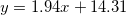
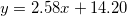
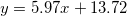
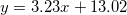
In this work, we found that the value of annealing temperature has an important effect on the morphology of CZO films. The CZO films annealed at 500°C have a minimum value of RMS roughness of about 7.056 nm. We found that the CZO films annealed at 500°C have the maximum value of optical density and the skin depth, especially in the low-energy range. It can be seen that the CZO films annealed at 500°C have a minimum value of the steepness parameter about of  but have a maximum value of electron-phonon interaction at about
  . The variations of
  of films vs. the
  were studied by the empirical equations linear fitting as
  , where 1.9 < A < 6 and 13 < B < 14.35. We observed that as-deposited CZO films have maximum values of dispersion energy (Ed
) at about 18 eV.
, where 1.9 < A < 6 and 13 < B < 14.35. We observed that as-deposited CZO films have maximum values of dispersion energy (Ed
) at about 18 eV.
Data availability statement: No new data were created or analysed in this study.