Abstract
In the past, the application of carbon nanotube-silicon solar cell technology to industry has been limited by the use of a metallic frame to define the active area in the middle of a silicon wafer. In our work, we use industry standard device geometries with a front- and back-junction design which allow for the entire wafer to be used as the active area. These are enabled by the use of an intermixed Nafion layer which simultaneously acts a passivation, antireflective and physical blocking layer as well as a nanotube dopant. This leads to the formation of a hybrid nanotube/Nafion passivated charge selective contact (PCSC) and solar cells with active areas of 1 – 16 cm2 are fabricated. Record maximum power conversion efficiencies of 15.2% and 18.9% are reported for front- and back-junction devices for 1 cm2 and 3 cm2 active areas, respectively. By placing the nanotube film on the rear of the device in a back-junction architecture many of the design related challenges for carbon nanotube silicon solar cells are addressed and their future application to industrialized processes are discussed.
Additionally, traditional silicon solar cells extract holes and achieve interface passivation with the use of a boron dopant and dielectric thin films such as silicon oxide or hydrogenated amorphous silicon. Without these two key components, few technologies have realized power conversion efficiencies above 20%. We now develop a carbon nanotube/Nafion ink that can be spin coated directly onto a silicon wafer to serve simultaneously as a hole extraction layer, but also to passivate interfacial defects. This enables a low-cost fabrication process that is absent of vacuum equipment and high-temperatures. Power conversion efficiencies of 21.4% on an device area of 4.8 cm2 and 20% on an industrial size (245.71 cm2) wafer are obtained.
[1] D. D. Tune, N. Mallik, H. Fornasier, B. S. Flavel, Adv. Energy Mater. 10, 2020, 1903261. DOI: 10.1002/aenm.201903261
[2] J. Chen, D. D. Tune, K. Ge, H. Li, B. S. Flavel, Adv. Funct. Mater. 2020, 30 2000484. DOI: 10.1002/adfm.202000484
[3] J. Chen, L. Wan, H. Li, J. Yan, J. Ma, B. Sun, F. Li, B. S. Flavel, Adv. Funct. Mater. 30, 2020, 202004476. DOI: 10.1002/adfm.202004476
[4] L. Wieland, H. Li, C. Rust, J. Chen, B. S. Flavel, Adv. Energy Mater. 2020 just accepted manuscript. DOI: 10.1002/aenm.202002880
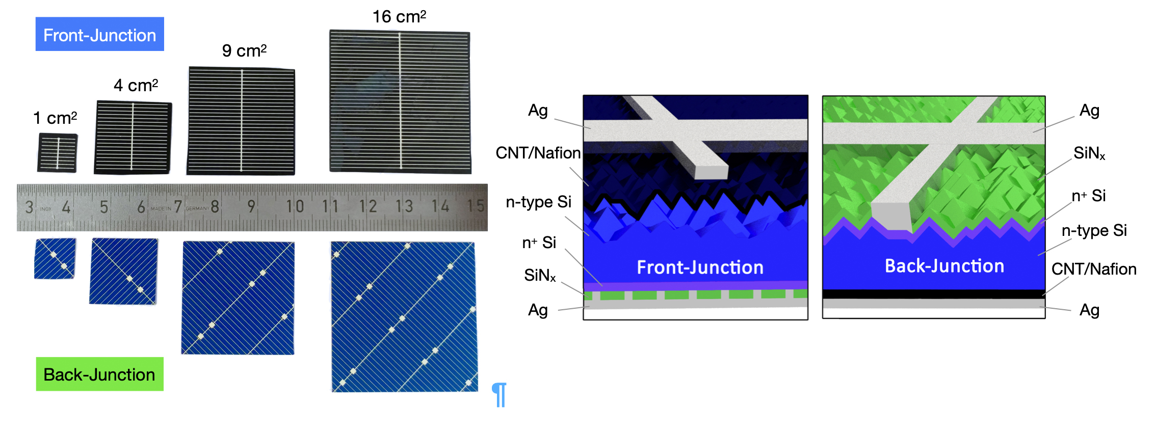
Figure 1