
Abstract
Contact resistivity reduction at the source/drain contacts is one of the main requirements for the fabrication of future MOS devices. Current research focuses on methods to increase the active doping concentration near the contact region in silicon-germanium S/D epilayers. A possible approach consists in adding co-dopants during the epitaxy process. In the case of p-MOS, gallium can be used in addition to boron. In this work, the properties of in situ Ga and B co-doped Si0.55Ge0.45 layers are discussed. The surface morphologies, layer compositions, structural and electrical material properties are described and compared with those of a B-doped Si0.55Ge0.45 reference layer. Ga segregation occurring at the growth surface is evidenced. Post-epi surface cleans are required to obtain the correct Ga profiles in the Si1−xGex layers from secondary ion mass spectrometry, otherwise altered by surface Ga knock-on. The layer morphologies, crystalline quality and electrical properties show a progressive degradation with increasing Ga dose. Finally, specific titanium-Si1−xGex:B(:Ga) contact resistivity values have been extracted using the multi-ring circular transmission line method. The contact resistivity is lower for the Ga co-doped samples, the best contact properties ( < 3 × 10⁻⁹ Ω.cm2) being obtained for the sample grown with the lowest Ga-precursor flow.
Export citation and abstract BibTeX RIS

This is an open access article distributed under the terms of the Creative Commons Attribution 4.0 License (CC BY, http://creativecommons.org/licenses/by/4.0/), which permits unrestricted reuse of the work in any medium, provided the original work is properly cited.
The miniaturization of transistors has resulted in several technology challenges. These include degradation in the carrier mobility within the channel, short-channel effects, and an increased contribution from parasitic resistances. 1,2 To overcome these issues, innovations in both the device materials and architectures had been required.
A great improvement in carrier mobility has been achieved through strained-Si technologies, introduced at the 90 nm technology node by Intel in 2003. 3 In pMOS devices, silicon germanium (Si1–xGex), epitaxially grown using Chemical Vapor Deposition (CVD), replaced Si as the Source/Drain (S/D) material. 4 The larger lattice parameter of Si1−xGex, in comparison to that of Si, induces a compressive strain in the channel region which leads to an enhancement in the hole mobility. 5
Concerning the device architecture, fin field-effect transistors (FinFETs) have successfully replaced planar FETs from the 22 nm node on. This device enabled improved electrostatic control of the carriers within the channel for reduced gate lengths, thereby leading to a boost in the device performances. 6
Due to the contact area (Ac) reduction in the S/D regions, the contact resistance (Rc = ρc/Ac, ρc being the specific contact resistivity) at the metal-semiconductor interface has become the most detrimental parasitic. Maintaining sufficiently low Rc for the upcoming (sub 5 nm) technology nodes therefore requires the formation of advanced contact engineering, setting important challenges on the control of S/D doping. 7 Increasing the active doping concentration in the epilayer near the contact region is the mainstream approach for achieving this objective. A high doping level narrows the depletion region within the semiconductor and, consequently, thins the Schottky barrier down. This favours carrier tunnelling through the contact and consequently results in a decrease in ρc.
Boron is the most commonly used p-type dopant for Si and Si1–xGex. When B dopants are placed in substitutional sites in the lattice, the compressive stress of pseudomorphic Si1−xGex is partially released. This is due to boron's smaller covalent radius, compared to those of Si and Ge. 8 This effect in turn enhances the dopant solid solubility in the Si1−xGex matrix with highest B levels typically obtained for Ge concentrations between 40% and 70%. 9 In addition, with the use of out-of-equilibrium low-temperature deposition processes with high growth rates, it is possible to achieve B active concentrations ([B]act) exceeding 1 × 10²¹ atoms cm–3 9 in strained Si1−xGex, while maintaining high crystalline quality. Such a B concentration is significantly higher than its solid solubility in Si. Nevertheless, a further increase in active doping concentration is needed to reach ρc values lower than 1 × 10⁻⁹ Ω.cm2, indicated as the requirement for the sub 5 nm technology nodes.
For this purpose, the investigation of new dopants is a research field worthy of interest. Gallium is considered a promising dopant for Si1−xGex alloys with high Ge concentrations for the following reasons: its solid solubility in Ge (5 × 10²⁰ at. cm−3) 10 is significantly higher than that of boron (2 × 10¹⁸ at. cm−3), 11 and it is a shallow acceptor both in Si (72 meV) and in Ge (11 meV).
In literature, Ti/Si1–xGex:Ga contacts with specific resistivities below 1 × 10⁻⁹ Ω.cm2 have already been reported. This was achieved by combining shallow ion implantation of a high dose of Ga and a subsequent nanosecond laser annealing. 12,13 Following the same approach, Tabata et al. demonstrated activation of Ga dopants up to 1.6 × 10²¹ at. cm−3 in Si0.5Ge0.5, 14 withstanding great promises for performance improvements in future devices. Using in situ doping, Xu et al. obtained B + Ga co-doped Si0.50Ge0.50 layers enabling ρc values as low as 5.7 × 10⁻¹⁰ Ω.cm2. 15 Compared to the ion implantation method, in situ doping techniques provide high activation levels without the need for any subsequent thermal budget. Other benefits include the possibility to grow the doped layers selectively with tailored doping profiles, 16 a key parameter in the formation of ultra-shallow junctions for advanced 3D structures such as gate-all-around (GAA), avoiding the shadowing effect which is typical for doping implantation. 17,18
In the present work, we explore epitaxially grown and in situ B and Ga co-doped Si1–xGex as a potential S/D material. The morphology, structural and electrical material properties of epilayers with different Ga contents are analysed and discussed. The specific resistivity of the Ti/Si1−xGex:B:Ga stacks are finally extracted and correlated with the layer properties.
Methodology
p-type Si1−xGex epitaxial layers with a nominal Ge content of 45% were externally grown using chemical vapor deposition (CVD) on blanket 300 mm n-type Si(001) substrates. 19 The samples include a B-doped Si1−xGex reference (sample R) and five Ga and B co-doped Si1−xGex epilayers (samples A, B1, B2, C, and D). Samples A, B1, B2, and C were grown targeting an increasing nominal Ga-content from A to C. Sample B1 and B2 have the same nominal Ga-level, but different thicknesses, with tB2 > tB1. Finally, sample D was grown with alternative process parameters compared to A, B1, B2, and C, targeting an increased Ga incorporation efficiency. The film thicknesses, ranging from 20 to 50 nm, were chosen to prevent strain relaxation.
Depth composition profiles were extracted for samples R, A, B1, and D through Secondary Ions Mass Spectrometry (SIMS). Sample B1 was analysed twice, (i) in its as-grown form and (ii) after a wet surface cleaning treatment consisting of a 10 min dip in a SC1-like solution of NH3, H2O2 and de-ionized water, followed by a 10 min dip in diluted HCl. Surface morphologies were inspected by top-view Scanning Electron Microscopy (SEM) using a KLA-Tencor eDR7100TM electron-beam wafer defect review system. X-ray reflectivity (XRR) and high-resolution X-ray diffraction (HR-XRD) scans were acquired with a Bruker JVX7300M diffractometer equipped with a Cu Ksα1 source (λ = 1.5406 Å) and a two-bounce Ge(220) monochromator. Epitaxial layer thicknesses were determined by both XRR measurements and HR-XRD Si(004) ω−2θ symmetric scans performed at 6 different locations along a wafer radius. HR-XRD data was also used to extract the out-of-plane lattice parameters of the epilayers. In case of defective layers (samples B2 and C), reciprocal space maps (RSM) were additionally acquired around the asymmetric Si(113) Bragg reflection in order to confirm the pseudomorphism of the Si1−xGex epilayers. Micro-four-point probe (m4pp) measurements were conducted using a Capres microHALL®-M300 system to obtain the sheet resistance (Rs) of the samples and estimate the resistivity of the grown layers. 20 Micro-Hall effect (MHE) measurements were performed using a Capres CIPTech®-M300. Collinear m4pp in the vicinity of an insulating boundary were performed on samples R and B1 (pre- and post- surface cleaning) to assess the holes concentrations (pH) and the Hall mobilities (μH),. 21,22 The contact resistivity of fabricated Ti/p-Si1−xGex contacts was finally assessed using multiring circular transmission line method (MR-CTLM) 23 structures patterned on top of the blanket epilayers. These structures are composed of 10 μm wide concentric metal rings separated by dielectric spacings with different widths, varying from structure to structure and ranging from 0.35 μm to 10 μm. The smallest structure has been inspected on one die of the reference wafer using cross-sectional transmission electron microscopy (X-TEM) to verify the achieved spacing width after the processing. The technique allows for ρc assessments down to the low 1 × 10⁻⁹ Ω.cm2 range. Multiple dies were measured on every wafer to improve the statistics.
Results and Discussion
This section summarizes the main features observed through the characterization of the B and Ga co-doped Si1−xGex epilayers. The first part presents evidence for a strong surface segregation of Ga during the epitaxy, as assessed through SIMS analysis. The second part discusses how Ga co-doping impacts the morphology and structural material properties of the epilayers. Finally, the electrical and contact properties are reported as a function of the Ga precursor flow used during the growth.
Chemical composition profiles and Ga segregation in Si1−xGex
The SIMS composition profiles, extracted as a function of depth, are presented in Fig. 1 for samples R, A, B1, and D. Unstable signals recorded in the first few nm are attributed to near-surface (depth < 5 nm) transient distortions. 24 This region of the layer will therefore be disregarded in the upcoming analysis.

Figure 1. B, Ge, Ga, and C chemical concentration profiles as a function of depth as measured by SIMS on samples: (a) R; (b) A; (c) B1; (d) D. The Ge percentage is plotted in linear scale (right axis), while the B, C, and Ga chemical concentrations are plotted in log scale (left axis). In d), a dashed horizontal line indicates a possible bulk-[Ga]chem value for sample D identified through an inflection point visible in the Ga curve.
Download figure:
Standard image High-resolution imageThe Ge concentrations (xGe) are reported using a linear scale (right axis) and are subject to error bars whose magnitude are difficult to evaluate. The Ge concentration in sample B1 was extracted twice using a different set of Si1−xGex standards in each run. This resulted in a difference between xGe values of 2 at.%. In the following discussions, this value will be adopted as an indicative error bar for the SIMS-measured Ge concentrations. In samples R and A, the Ge concentrations are constant throughout the layers depth and are close to the 45% target value. The Ge content is lower in sample B1 and slightly decreases when moving towards the surface (from 43.5% at the layer/substrate interface to 42.5%, just below the surface peak). In sample D, a more pronounced decrease in Ge concentration is observed (from 50%, before the overshoot near the substrate, down to 42%, near the surface). Ge profiles with similar gradients have been observed before in Ga-doped and B + Ga co-doped Si1−xGex. 25 The formation of a Ge gradient might be associated with the co-flow of Ga-precursors.
Boron concentration profiles ([B]chem) are flat at ∼ 1 × 1021 cm−3 in all the measured samples, except for sample D, where the B level gradually decreases from a maximum of 6 × 1020 cm−3, close to the interface with the substrate, down to 4.5 × 1020 cm−3 in the near-surface region. However, due to the gradient in xGe reported for this layer, the sputtered matrix gradually changes during the analysis, possibly leading to variations in the B quantification.
The Ga chemical concentration ([Ga]chem) profiles, displayed for samples A, B1, and D in Fig. 1, appear graded, with increasing level when moving towards the surface. Abrupt concentration peaks are observed in the first 2 nm from the surface, yet transient effects obstacle the correct elemental quantification at the surface proximity. To verify the actual incorporation of Ga in the epilayer, a piece of sample B1 was cleaned with the basic solution described in the experimental section and remeasured. The comparison of the SIMS profiles between the layer in its as-grown form and after the surface cleaning is shown in Fig. 2. A variation in thickness of ∼ 2 nm due to the cleaning treatment can be estimated by overlapping the two B profiles. The B bulk levels remain unchanged, while the extracted Ga profile is dramatically impacted, with a significant reduction in Ga concentration after the cleaning. This decrease is visible (i) near the surface, and (ii), also in the bulk part of the layer. The surface decrease is explained by the removal of the Ga-rich top layer formed on the as-grown surface. This result confirms that during epitaxy, Ga accumulates at the growth front and the large gradient in Ga concentration towards the surface is not real. The decrease in bulk Ga concentration evidences the occurrence of a SIMS artefact caused by Ga knock-on during sputtering (recoil mixing). 26,27 The Ga dose which is detected when no surface clean is applied, therefore originates mainly from the sample surface, with only a small fraction of it being incorporated in the bulk region, with a saturation level below 1 × 10¹⁸ at. cm−3. The real Ga profile therefore presents a steep surface peak (removed with the surface clean), followed by a lowly doped region and a zone fully depleted of dopants adjacent to the interface with the substrate. As described by Greene et al., this profile is characteristic of layers doped with elements exhibiting a strong segregation tendency. 28 For sample B1, the fractions of dopants present at the surface and within the bulk region, respectively, can be estimated by integrating the two recorded profiles as measured before and after the clean. Following such an approach, a total Ga dose of 2.7 × 10¹³ at. cm−2 is obtained before clean, of which only 7 × 10¹¹ at. cm−2 is incorporated within the layer (after clean, i.e. ∼ 3% of the total). The estimated total Ga doses for the other samples are reported in Table I. The quantification of the superficial Ga may be incorrect since Ga is not incorporated in a Si1−xGex matrix but is likely present over the surface in a different phase. The calculated doses can still be used for relative comparison among the samples. Finally, the Ga profile measured in sample D presents an inflection point at around 25 nm from the surface (Fig. 1d). A probable explanation is that, from that point on, the bulk Ga signal emerges from the decaying tail originated at the surface. This would result in a bulk concentration of ∼5 × 10¹⁸ at. cm−3, significantly higher than the bulk Ga level measured in sample B1 (<1 × 10¹⁸ at. cm−3).
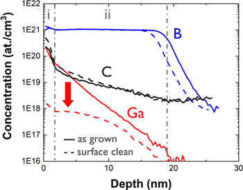
Figure 2. B, C and Ga chemical concentration profiles extracted from sample B1 - as-grown (continuous lines) and after a surface clean (dashed lines). The red arrow highlights the Ga loss due to the applied surface clean. The labels placed on top part of the figure indicate (i) the near-surface region of the layer, and (ii) the bulk region of the layer.
Download figure:
Standard image High-resolution imageTable I. Thicknesses and RMS roughness values as obtained from XRR spectra, thicknesses and xGe,app as extracted from XRD ω−2θ scans, and Ga doses obtained from SIMS data. *A Ga dose > 2.7 × 10¹³ at cm−2 is expected for sample B2 since the same Ga precursor flow as in B1 was used for a longer deposition time. The label "grad." indicates the presence of a concentration gradient. Values between brackets correspond to the concentration values at the bottom and at the surface of the layer, respectively.
| Sample | Ga-prec. flow (a.u.) | tSiGe,XRR (nm) | rRMS,XRR (nm) | tSiGe,XRD (nm) | xGe,app XRD | xGe,SIMS (%) | [Ga]2D,SIMS (at. cm−2) | [B]chem, SIMS (at. cm−3) |
|---|---|---|---|---|---|---|---|---|
| R | 0 | 37 ± 0.5 | 0.5 | 38 | 0.345 | 45 ± 2 | 0 | 9 × 10²⁰ |
| A | 0.2 | 22 ± 0.5 | 0.5 | 21 | 0.346 | 46 ± 2 | 5.4 × 10¹² | 9 × 10²⁰ |
| B1 | 0.5 | 21 ± 0.5 | 0.6 | 20 | 0.340 | Grad. [43.5–42.5]±2 | 2.7 × 10¹³ | 1 × 10²¹ |
| B2 | 0.5 | 45 ± 0.5 | 1.4 | 44 | 0.330 | NA | NA | NA |
| C | 1 | 32 ± 0.5 | 3.7 | 30 | 0.325 | NA | NA | NA |
| D | NA | 48 ± 0.5 | 0.4 | 47 | 0.362 | Grad. [50–43]±2 | 1.9 × 10¹⁴ | Grad. [6–4.5] × 1020 |
Carbon might be unintentionally incorporated within the Ga-doped layers due to the C-containing groups present in the Ga metal-organic precursor. The presence of adventitious C on the sample surfaces, however, has a significant impact on the C profiles shown in Figs. 1a–1d. This is confirmed by C being detected in the first 20 nm of the reference layer, which was grown without any C-containing precursor. Furthermore, beyond 20 nm in depth, the measured C concentrations in all layers are lower than those in the underlying substrates. This indicates that the C concentration in the reported samples is negligible and likely lower than the C SIMS detection limit (∼1 × 10¹⁸ at. cm−3).
Morphology and X-ray analysis
Figure 3 shows top-view SEM images and XRR spectra acquired on the samples at wafer center. Arbitrary vertical offsets have been applied to the XRR curves to enable a sample-to-sample comparison. Samples R, A, and B1 exhibit smooth surfaces (Fig. 3a). This is also confirmed by XRR which shows clear Pendellösung fringes for the full spectra. For these three samples, a similar root mean square roughness (rRMS) of around 0.5 nm is obtained (Table I). Thus, despite the high B concentration in the Si1−xGex layers, an enhancement of surface roughening does not occur. The surfaces of samples B2 and C, however, are rougher, with estimated rRMS values of 1.4 and 3.7 nm, respectively. Although samples B1 and B2 were grown with identical process parameters (except for the deposition time), B2 exhibits a significantly rougher surface. This can be explained by the higher Ga surface concentration in this sample, due to longer Ga accumulation during the epitaxy. The epilayer in sample C was grown with the highest Ga precursor flow, resulting in a high Ga surface concentration and a consequent surface roughness. Sample D has the highest Ga dose among the samples measured by SIMS, but it still has a smooth surface morphology (rRMS = 0.4 nm), indicating that the amount of surface-segregated Ga in this sample is limited. In samples B2 and C, we expect higher Ga doses. Sample thicknesses as extracted from XRR spectra fitting are reported in Table I.

Figure 3. (a) top-view SEM images acquired at the center of the wafers. Samples B2 and C present an evident surface roughness, while the surfaces of samples R, A, B1, and D are smooth; (b) Corresponding XRR spectra. Offsets have been applied to ease the comparison between samples. Thickness fringes are observed for all samples, albeit the higher roughness of sample C quickly attenuates the signal.
Download figure:
Standard image High-resolution imageHR-XRD ω−2θ scans acquired around the (004) Bragg reflection are shown in Fig. 4a. Again, arbitrary offsets were applied to the curves to ease sample-to-sample comparison. Pendellösung fringes located on both sides of the Si1−xGex diffraction peaks are observed for all the samples. Their presence provides a first indication that the layers are strained. The thicknesses extracted using the side fringes are in good agreement with the values obtained from XRR (Table I). The out-of-plane lattice parameters (a⊥) of the different samples were derived from the Si1−xGex peak positions and used to determine the Ge content in the layers as described in the following.

Figure 4. (a) HR-XRD ω−2θ scans. The vertical dashed line is centered at the Si1−xGex diffraction peak of sample R to guide the reader's eye through the variations in peak positions. The blue arrow highlights the progressive increase in Ga dose from sample R to C; (b) apparent Ge concentration (xGe,app) as extracted by fitting the HR-XRD spectra without including the substitutional B in the model; (c) Reciprocal space maps acquired in the vicinity of the asymmetric Si(113) Bragg reflection for samples B2 and C.
Download figure:
Standard image High-resolution imageIn undoped Si1−xGex layers, the relaxed lattice constant is determined by the modified Vegard's law: 29,30

where aSi(1−x)Gex, aGe and aSi are the lattice constants of relaxed Si1−xGex, Ge, and Si, respectively. The last term of the expression corresponds to the deviation from the pure Vegard's law and b = 0.0272 is the bowing parameter. The samples reported herein were targeted to be fully strained (pseudomorphic). In this case, the Si1−xGex has a tetragonally distorted unit cell, with the in-plane (a∣∣) and out-of-plane (a⊥) lattice constants expressed as follows: 17

where k ∼ 1.75. Once a⊥ is measured, the xGe concentration in the alloy is obtained through:
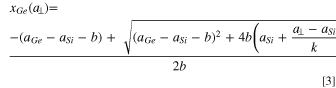
The extracted apparent Ge concentrations are reported in Fig. 4b and Table I. The apparent Ge concentrations (xGe,app) extracted in this way do not account for the presence of substitutional boron in the layers. Substitutional B, in fact, induces a shrinkage of the Si1−xGex lattice parameter causing a shift of the diffraction peak towards the Si substrate peak. The measured apparent Ge concentrations will thus result in lower values compared to the real value. A decrease in xGe,app is noticed by comparing samples R and A with samples B1, B2, and C. More specifically, for B1, B2, and C, xGe,app decreases with the dose of Ga-precursor flown during the epitaxial growth. This decrease corresponds to a reduction in the out-of-plane lattice parameters for these samples, that might be caused by several factors: (i) an increase in substitutional B concentration, (ii) a decrease in Ge concentration, or (iii) the onset of plastic strain-relaxation. However, the available SIMS data does not show differences in [B]chem for samples R, A, and B1, and the electrical characterization of the layers (discussed in the next section) rules out the possibility of different activation levels, that should otherwise be visible from the resistivity and the Hall carrier concentration data. Our observations suggest that the decrease in Ge concentration (ii) with the increase in Ga-precursor flow is a more likely explanation. Sample D was grown with a different set of process conditions and shows a higher xGe,app. According to the SIMS spectra (Fig. 1d), [B]chem is lower in sample D. In addition, the gradient in the xGe profile is larger than in the other samples and it starts from a higher concentration near the substrate. This explains the higher xGe,app. Finally, the absence of strain-relaxation—proposed cause (iii)—has been verified with reciprocal space maps, acquired on both samples B2 and C around the asymmetric (113) Bragg reflection (Fig. 4c). These two samples were chosen because of their non-ideal surface morphologies. In both maps, the Si1−xGex:B:Ga and the Si substrate peaks exhibit the same h(110) value, meaning that the in-plane lattice parameters of the epitaxial layers and of the underlying substrate are equal. Both layers are therefore fully strained, thus confirming the interpretation of the thickness-fringes visible in the ω−2θ scan spectra. However, in Fig. 4c halos are noticed around the Si1−XGeX:B:Ga diffraction peaks. Their presence may be explained by a certain degree of defectivity introduced by the doping with Ga.
In addition, the main Si1−xGex diffraction peaks acquired on samples B2 and D present some variations in shape if compared to the spectra corresponding to samples R, A, B1. This difference is explained by the graded Ge concentration within these epilayers—as observed in the SIMS spectrum of sample D (Fig. 1d). xGe progressively decreases by moving from the interface with the Si substrate towards the surface. If a graded Ge concentration profile is considered within the XRD simulation model, it results in an excellent match between the simulated curve and experimental data (Fig. 5). With this method the gradients in Ge concentration can be estimated. The extracted differences between surface and bottom xGe values are ∼ 6 and 7.5 at.% for sample B2 (Fig. 5a) and D (Fig. 5b), respectively. The latter is in nice agreement with the variation of Ge extracted from SIMS (8 at.%). In addition, sample D presents an asymmetric peak shape. This is well fitted if the Ge overshoot near the interface with the substrate (Fig. 1d) is also taken into consideration within the XRD fitting model. Finally, an even broader diffraction peak as seen for sample C (Fig. 4a), which can be explained by the higher defectivity. This renders the interpretation of the peak shape too ambiguous to extract any meaningful information from it.
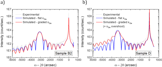
Figure 5. curve fitting of HR-XRD ω−2θ spectra of samples: (a) B2 and (b) D. Two different xGe distributions are considered in the simulation models: a constant xGe concentration through the layer (blue line) and a graded xGe profile, with a higher Ge content near the layer/substrate interface that decreases when moving towards the layer surface (red line). The simulated spectra generated from the second model show an improved matching with the experimental curves.
Download figure:
Standard image High-resolution imageAs mentioned above, a high substitutional boron concentration ([B]sub) influences the Si1−xGex diffraction peak position in the XRD spectra. The magnitude of the recorded shift can be used to estimate the concentration of substitutional boron [B]sub. 31 For a certain boron molar fraction (y), the relaxed lattice parameter for Si1−x−yGexBy is given by: 32
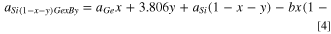
where the contraction factor of 3.806 accounts for the substitutional B present in the layer. Then, for pseudomorphic B-doped Si1−xGex, expression (2) becomes:

with k again assumed to be equal to 1.75. If the x value is known from other characterization techniques, it is possible to estimate the substitutional boron concentration from the measured out of plane lattice parameter through:
For Si1−xGex this procedure is not straightforward as the assumed xGe values deeply impact the [B]sub estimated in this way. To extract [B]sub, the Ge concentrations as measured by SIMS were therefore used. An inaccuracy in [B]sub of ±1.3E20 cm−3 is estimated considering the aforementioned uncertainty of 2 at.% in the xGe quantification. It is consequently impossible to draw an accurate trend with this approach, but for all samples a [B]sub value within the range 6–7.5 × 10²⁰ at. cm−3 was extracted. This implies an almost full activation of B in sample D but a small fraction of inactive B in the remaining samples.
Electrical characterization and contact resistivity measurements
The resistivity (ρ) of the samples is calculated from the sheet resistance and the film thickness as measured at the center of the wafers. A 0.1% relative error in Rs is considered. 33 Figure 6a shows the resistivity values of samples R, A, B1, B2 and C, as a function of the Ga precursor flow used during epitaxial growth. The resistivity is found to increase by increasing the Ga precursor flow. Samples B1 and B2 show very similar resistivity values, despite the more degraded morphology observed for B2 (Fig. 3a). A possible explanation for the observed increase in ρ with Ga precursor flow is that the material crystallinity is affected by the Ga segregation mechanism which introduces defects leading to a degradation in carrier mobility. In addition, a depletion region is formed at the p-n junction at the interface between the epilayer and the substrate, slightly narrowing the electrical thickness in the layer. This has the largest impact on the thinnest layers (A, B1), causing the measured ρ to be higher. Figure 6b shows the measured resistivity as a function of [B]chem as measured by SIMS. For samples B2 and C, a [B]chem of 1 × 1021 cm−3 has been assumed. Literature data for Si1−xGex:B (0.3 ≤ × ≤ 0.5), 32,34–36 and the resistivity of an in-house processed B-doped Si0.50Ge0.50 layer (labelled as "Lowly doped Si0.50Ge0.50:B") are added for comparison. The resistivity of sample R aligns with the trend defined by the literature data, while the data points for the Ga-containing samples A, B1, B2, and C are placed above the trendline. Sample D, which has a smooth surface morphology and is the thickest sample in this study, has its ρ value in line with the trend. The different process conditions used for the growth of this sample seem to mitigate the detrimental effect of Ga-doping on material resistivity.

Figure 6. (a) resistivity (ρ) values obtained at the wafer center for samples R, A, B1, B2 and C and plotted as a function of the Ga precursor flow in arbitrary units. (b) ρ plotted as a function of [B]chem for samples R, A, B1, B2, C and D. Datapoints have been added from the literature and from in-house produced samples. The dashed line indicates the expected trend for ρ vs [B]chem.
Download figure:
Standard image High-resolution imageMicro-Hall effect (MHE) measurements were performed on samples R and B1 to extract and compare the Hall carrier concentrations (pH ) and the Hall mobilities (μH). Sample B1 was measured before and after the surface cleaning described in the experimental section to identify any possible impact of the surface-Ga removal on the measured carrier concentration. The Hall scattering factor (rH), not precisely known, was considered equal to 1. This may lead to an overestimation of the measured carrier concentration. To determine the error bars on the pH values, an uncertainty of 0.5 nm was considered for the XRR-extracted thicknesses and the 3-sigma variation (3σN) over a 5-point average for the Hall-dose (NH). The relative standard deviation for NHS and μH is similar in magnitude to the values reported in. 37 The results are shown in Fig. 7 with the measured pH values found to be similar for all samples. The surface cleaning was found to have no significant impact on the carrier concentration, meaning that the segregated Ga sits inactive on top of the layer surface. On the other hand, for the Ga + B co-doped samples, the mobility is lower than for the B-doped reference. Combining these results with the ρ measurements (Fig. 6a), SEM inspections (Fig. 3a), and the RSM acquired on samples B2 and C (Fig. 5), where higher Ga-doses were deposited, it can be suggested that the Ga add-on causes a degradation of the material crystalline quality, which influences carrier scattering and, in turn, the hole mobility.
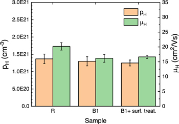
Figure 7. hole concentration (left axis) and Hall mobility (right axis) as extracted via MHE measurement for samples R, B1 as-grown and B1 after a surface clean, considering a Hall scattering factor of 1. A mobility reduction is observed in Si1−xGex:B:Ga vs Si1−xGex:B. Active carrier concentrations are, within the experimental error bars, the same.
Download figure:
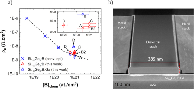
Standard image High-resolution imageMR-CTLM structures were finally fabricated to evaluate the specific contact resistivity of Ti/Si1−xGex:B(:Ga) contacts. A possible source of error in this measurement is the deviation of the dielectric spacing width from the nominal dimension that may significantly affect the extracted contact resistivity. Therefore, the width of the dielectric spacings between the concentric metal rings has been measured by inspecting one of the smallest MR-CTLM fabricated structures with X-TEM, as shown in Fig. 8b. A 3% inaccuracy in the spacing width measurement is considered and it is used to estimate error bars on the extracted ρc values.
Figure 8. (a) Ti/p-Si1−xGex contact resistivity values as a function of [B]chem. The blue crosses refer to in-house Si1−xGe1−x:B epilayers grown with conventional precursors. The triangles indicate the samples of this work. An experimental trendline of ρc vs [B]chem for Si1−xGex:B/Ti contacts 38 is indicated with dashed lines. (b) Cross-section TEM image of a dielectric region between two concentric metal rings in the smallest MR-CTLM structure.
Download figure:
Standard image High-resolution image
ρc is plotted as a function of [B]chem in Fig. 8a, and extracted values are summarized in Table II. Figure 8a also includes internal data from Si1−xGex:B epilayers with several [B]chem values (range: 4.6 × 10¹⁸–1 × 1021 cm−3) measured using the same MR-CTLM scheme as this work. In addition, the ρc vs [B]chem trendline for Si1−xGex:B/Ti contacts reported in 38 is plotted. Surprisingly, the value of ρc in the Si1−xGex:B reference sample (R) is much higher than the expected value (measured to be ∼ 9 × 10⁻⁹ Ω.cm2, while expected to be ∼2 × 10⁻⁹ Ω.cm2). We believe this data point is an outlier due to a non-optimal CTLM fabrication process for this specific sample. In fact, the anomalous ρc measured is not explained by characterization results from sample R.
Table II. Rs, ρc, and ρ as extracted from MR-CTLM data fitting, ρ obtained combining m4pp and XRR measurements, and pH and μH, obtained from MHE and XRR measurements.
| Sample | tSiGe,XRR (nm) | Rs ( Ω/sq.) | ρc (Ω.cm2) | ρMR-CTLM (Ω.cm2) | ρm4pp (Ω.cm) | pH,MHE (cm−3) | μH,MHE (cm−2 Vs−1) |
|---|---|---|---|---|---|---|---|
| R | 37 ± 0.5 | 59.4 ± 0.1 | 8.6 ± 0.9 × 10⁻⁹ | 2.4 × 10⁻⁴ | 2.2 ± 0.03 × 10⁻⁴ | 1.4 ± 0.1 × 10²¹ | 20.2 ± 1.2 |
| A | 22 ± 0.5 | 148.4 ± 0.2 | 2.8 ± 0.7 × 10⁻⁹ | 3.2 × 10⁻⁴ | 3.3 ± 0.08 × 10⁻⁴ | — | — |
| B1 | 21 ± 0.5 | 161.2 ± 0.2 | — | — | 3.4 ± 0.08 × 10⁻⁴ | 1.3 ± 0.1 × 10²¹ | 16.2 ± 1.3 |
| B2 | 45 ± 0.5 | 73.3 ± 0.1 | 3.2 ± 0.4 × 10⁻⁹ | 3.3 × 10⁻⁴ | 3.3 ± 0.04 × 10⁻⁴ | — | — |
| C | 32 ± 0.5 | 127.9 ± 0.1 | 3.7 ± 0.7 × 10⁻⁹ | 4.1 × 10⁻⁴ | 4.1 ± 0.07 × 10⁻⁴ | — | — |
| D | 48 ± 0.5 | 75.5 ± 1 | 4.1 ± 0.6 × 10⁻⁹ | 3.6 × 10⁻⁴ | 3.6 ± 0.04 × 10⁻⁴ | — | — |
Among the Ga co-doped samples, the best contact properties are achieved for the lowest Ga dose (sample A), with a measured ρc below 3 × 10⁻⁹ Ω.cm2. In samples B2 and D, the increase in Ga dose and consequent morphology degradation, are correlated with an increase in contact resistivity and a deviation from the trend. In sample D, the morphology is not affected by the Ga surface accumulation and the ρc formed at the Ti - semiconductor –interface lies on the trendline from. 38
It is worth highlighting that the layer thickness is not the same for all the samples, as summarized in Table II. In a recent study, 34,39 we demonstrated that the thickness of Si1−xGex:B films is a parameter affecting the specific resistivity of the Ti/Si1−xGex:B contacts. In particular, a decrease in B incorporation was observed when the B-doped Si1−xGex layer relaxes during epitaxial growth. However, from the different characterizations performed on the current samples, no evidence of strain relaxation was found. Also, the B SIMS profiles do not show any significant decrease towards the surfaces, as oppositely observed for the relaxed Si1−xGex:B samples in the aforementioned references.
None of the Ga + B co-doped samples presented here exhibits a ρc below the trendline of Fig. 8a. Based on the results of this work, we cannot claim beneficial effects on the p-Si1−xGex/Ti contact properties linked to the Ga add-on. On the contrary, Ga surface segregation seems to cause a degradation of the material and contact properties, once a critical Ga superficial dose is exceeded. However, it must be reminded that the Ga incorporation is quite poor in the epilayers here reported. By finding ways to control the dopant segregation, improvements in electrical and contact properties may be achieved by means of Ga in situ doping.
Conclusions
We discussed the material and contact properties of in situ B and Ga co-doped Si1−xGex layers epitaxially grown on Si(001) by means of chemical vapor deposition and with a nominal Ge content of 45%. The main process variable was the Ga precursor flow, which has been varied to modulate the Ga dose incorporated in the grown materials. All the layers were confirmed as fully strained with respect to the Si(001) substrate. However, for high Ga doses, certain degrees of crystalline disorder and surface roughening was observed.
Without surface cleaning, a graded Ga concentration profile was measured, with a Ga-rich region close to the sample surface and a decrease in Ga concentration towards the bottom Si1−xGex/Si interface. The correct bulk Ga profile was unveiled from SIMS measurements following a wet-chemical treatment of the sample. Without this surface treatment, Ga knock-on during SIMS surface sputtering resulted in a severe overestimation of the Ga content within the epitaxial layer. For this set of samples, most of the Ga segregated towards the surface, while the bulk Ga level saturated at very low concentrations. Consequently, the Ga co-doping did not significantly change the overall carrier concentration, although it did reduce the Hall mobility. As a result, the resistivity increased with increasing Ga precursor flow.
The Ga add-on is associated with the formation of a gradient in Ge concentration. The Ge/Si ratio diminishes when moving from the substrate to the layer surface. The variation in Ge incorporation during the epilayer growth may be attributed to the progressive accumulation of Ga atoms at the surface.
Finally, the lowest contact resistivity value of below 3 × 10⁻⁹ Ω.cm2 was obtained for Ti/Si1−xGex:B:Ga contacts formed on an epilayer with [B]chem of 1 × 10²¹ at. cm−3 and a limited Ga content. However, in terms of contact properties, the reported Ga co-doped samples did not outperform conventional Si1−xGex:B epilayers with comparable [B]chem levels. This study, therefore, did not demonstrate a reduction in contact resistivity promoted by the Ga add-on. Ga surface segregation, on the contrary, appears to affect the material structural and electrical properties resulting in a degradation of the final contact performance. Still, the characterization of a sample grown with alternative process conditions has shown that there is room to enhance the Ga bulk concentration in the layers while keeping the material quality under control. Due to its segregation tendency, understanding and controlling Ga incorporation is a challenging task, but improvements in this sense may unfold new approaches to overcome the current limits in active doping levels in S/D regions.
Acknowledgments
G. Rengo acknowledges the Research Foundation of Flanders (FWO) for granting him a PhD fellowship strategic basic research. The imec core CMOS program members, European Commission, local authorities and the imec pilot line are acknowledged for their support. This project has received funding from the ECSEL Joint Undertaking (JU) under grant agreement No 875999. The JU receives support from the European Union's Horizon 2020 research and innovation programme and Netherlands, Belgium, Germany, France, Austria, Hungary, United Kingdom, Romania, Israel.