

Abstract
Recent advances in graphene nanoribbon (GNR) field-effect transistors (FETs), with finite band-gap, have shown great promise for their use in ultra-scaled, low power and high speed device applications. Here, we use quantum mechanical simulations, based on non-equilibrium Green's function (NEGF), to study the electrical characteristics of a sub-10 nm gate length GNRFET with double gate structure. Tight-binding approximation is used to extract the energy bands of GNR and the results are validated with density functional theory (DFT) calculations. Key electrical parameters are computed for different dielectric material, source/drain doping and temperature combining the channel length scaling beyond 10 nm to study performance variation. Results reveal that change in source/drain doping shows significant impact on performance for shorter channel, while the opposite tendency is observed for dielectric constant (k) variation. GNRFET showed robustness against temperature variation compared to conventional Si devices. Finally, the results were benchmarked against the performance metrics of high performance and low power CMOS devices in the 5-nm technology node. A significant rise in leakage current beyond the LP requirement was observed for gate lengths below 5 nm. Results obtained from this study can provide useful insights in the design and implementation of next generation GNRFETs.
Export citation and abstract BibTeX RIS
Graphene, with its atomically thin two-dimensional (2D) structure, has been explored extensively, as a potential alternative to Si, to continue gate length (LG ) scaling beyond 10 nm. 1,2 In addition to potentially achieving ultimate scaling, graphene offers high carrier mobility, longer mean free path and weaker electron-phonon interaction which enables graphene devices to outperform Si transistors in terms of intrinsic speed. 3,4 However, lack of bandgap in pristine graphene, makes it difficult to turn off graphene FETs, thereby limiting its use in future logic devices. The issue can be overcome by using edge terminated narrow strips of graphene, known as graphene nanoribbons (GNR),which acquire a bandgap through quantum confinement in transverse direction. 5,6 Experimental studies on GNRFETs are often challenged by the limitations in current device fabrication technology. 7,8 Moreover, there are several bottlenecks in integrating GNR into the present CMOS technology nodes, while maintaining The International Roadmap for Devices and Systems (IRDS) requirements for high performance (HP) and low power (LP) integrated circuits. 9,10 To address the challenges in ultra-scaled dimension and design efficient systems for future technology nodes with GNRFETs, computational studies are required to quantify and benchmark performance variation owing to changes in device design. Recent reports have explored scaling effect 11,12 as well as influence of individual device parameters and their exploitation strategies for performance enhancement 13–16 on GNRFETs. However, combining the effect of device parameters such as source/drain doping concentrations, dielectric material, and temperature with channel length (LG ) scaling in sub-10 nm regime, under a single simulation platform is yet to be investigated. This is necessary not only to evaluate its practicality but also to determine optimal design criteria for better experimental results beyond the scaling limit of conventional technology.
In this work, electrical performance of a double-gated (7, 0) armchair GNRFET has been studied with different source/drain doping concentrations, dielectric material, and temperature. All simulations are carried out for sub-10 nm channel lengths to include the effect of extreme scaling. Moreover, the simulation results have been benchmarked against the performance metrics for CMOS HP and LP devices for the 5-nm technology node. Quantum mechanical simulations have been used to incorporate direct source-to-drain tunneling and band-to-band tunneling (BTBT), which are the dominant mechanisms in deep subthreshold region of sub-10 nm FETs. The model is based on self-consistent iterative solution of two-dimensional Poisson equation and one dimensional Schrödinger equation within the non-equilibrium Green's function (NEGF) formalism in decoupled mode space representation to reduce computational burden. 17 Nearest neighbor tight-binding (TB) method, with an atomistic Pz orbital basis set, is implemented to account for lateral confinement as well as for computing the energy of the sub-bands. Results from TB model have been validated with first-principles Density Functional Theory (DFT) calculations. Carrier transport in the longitudinal direction is solved by constructing an energy-position dependent Hamiltonian, with non-parabolic effective mass compensation, and treating the problem within the NEGF for each sub-band.
The remainder of the article is organized as follows; the Simulation Approach section introduces the simulated device structure and discusses the computational framework with respect to relevant equations. Results and Discussion section presents the simulation results and performance benchmarking, followed by the Conclusion.
Simulation Approach
A double gated GNRFET, as shown in Figs. 1a–1b, is considered in our simulation. (7,0) armchair GNR (AGNR), which can be fabricated by bottom-up approach with precise edges,
7,18
is taken as the channel material. The GNR is placed between two layers of insulator with a thickness tox
= 1.5 nm. The length of heavily doped n-type source and drain regions are equal to the length of intrinsic GNR channel. This reduces the probability of gate-induced drain leakage (GIDL).
19
The source/drain regions are assumed to be uniformly doped with a doping concentration of NS/D
. The width of the channel is essentially that of the GNR and is given by  where
where  is the number of dimer lines in the transverse direction and
  is the carbon-carbon bond length. A power supply voltage of VDD
= 0.65 V is used for performance analysis of the GNRFET.
is the carbon-carbon bond length. A power supply voltage of VDD
= 0.65 V is used for performance analysis of the GNRFET.
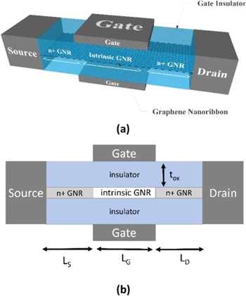
Figure 1. (a) 3D Structure of the double gate GNRFET. GNR is sandwiched between two thin layers of insulator. The length of the channel (intrinsic GNR) and the doped source/drain extension is kept equal (b) simplified 2D representation of the structure.
Download figure:
Standard image High-resolution imageNearest neighbor tight binding (TB) model, with orthogonal Pz orbital basis set, is used to extract the energy eigenvalues and dispersion relation of carriers in GNR. A matrix element of the TB Hamiltonian, indicating the interaction between the αth atom in the pth slab and βatom in qth slab, is given by:

Where  is the potential at (p, α) atom site and
  is the Kronecker delta. The parameter
  is the nearest neighbor hopping energy, which equals −2.7 eV if the atoms (p, α) and (q, β) are nearest neighbors and equals zero otherwise. For the atoms along the edges of the ribbon t is incremented by a factor of (1 + δ), with δ = 0.12.
5
The non-linearity of the bands near the Dirac point is corrected by the effective mass model given by
20
as,
is the nearest neighbor hopping energy, which equals −2.7 eV if the atoms (p, α) and (q, β) are nearest neighbors and equals zero otherwise. For the atoms along the edges of the ribbon t is incremented by a factor of (1 + δ), with δ = 0.12.
5
The non-linearity of the bands near the Dirac point is corrected by the effective mass model given by
20
as,
Where  is the energy,
  is the energy bandgap and
  is the effective mass for a particular sub-band index n.
We have also calculated the dispersion relation using DFT, as shown in Fig. 2, to verify the accuracy of our TB model. DFT, along with the highly accurate projector augmented wave (PAW) method, with a plane wave cutoff of 400 eV, as implemented in the Vienna ab initio simulation package (VASP) 21 has been used. The spin-restricted generalized gradient approximation (GGA) with the Perdew–Burke–Ernzerhof functional (PBE) 22 and the hybrid functional (HSE06) 23 techniques and PAW methods, are used to study (7,0) AGNR. The bandgap extracted from the TB model is 1.53 eV, which matches very well with the DFT calculated one. Also, the energy dispersion relation matches reasonably well near the energy minima, where the population of carriers is maximum. This high value of bandgap leads to inherently high IOn /IOff ratio for the armchair (7, 0) GNR structure. The transport calculations in the longitudinal direction is done using the NEGF formalism for each sub-band. Only first two sub-bands were considered in the simulation as the contribution of higher sub-bands are negligible for the carrier transport in (7, 0) a-GNR. The device Hamiltonian is constructed with a discretization step of 3dc-c and a correction for non-parabolic band diagram employed by a position dependent effective mass model. This has been described in 20 and can be presented as follows:
Where  represents the effective mass of kth sub-band while
 and
and  are the valence band, conduction band and the intrinsic Fermi level along the longitudinal direction respectively. With the constructed matrix, the retarded Green's function for a particular sub-band is obtained as follows:

Where E denotes the energy, I is the identity matrix,  and
and  represents the self-energy matrices of source and drain contacts respectively.
  and
and  are the only non-zero elements of the self-energy matrices which have been obtained by the relations described by Datta.
24
are the only non-zero elements of the self-energy matrices which have been obtained by the relations described by Datta.
24
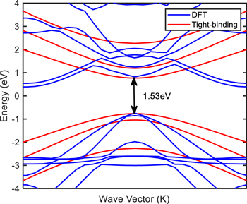
Figure 2. Dispersion relation of (7, 0) AGNR extracted from tight-binding and DFT calculations. Tight-binding parameters were taken as t = 2.7 eV and δ = 0.12.
Download figure:
Standard image High-resolution imageThe energy level broadening quantities, introduced by the source and drain contacts for the kth sub-band, are obtained by:


The mobile charge density due to electrons and holes, along transport direction, is extracted using the local density of states with the Fermi function of the source/drain contacts, by taking summation over all the considered sub-bands:
Where  is the Fermi–Dirac distribution of source and drain contacts and
  is the wave function of kth sub-band. This mobile charge density is used to calculate the net charge density along the channel with the help of the charge neutrality equation:

Where q is the magnitude of an electron's charge and 
 and
and  denote the spatial distribution of the concentration of holes, electrons, donors and acceptors respectively The electrostatic potential distribution, employing Poisson equation, is given by:

The continuous form of this equation is discretized by means of finite difference scheme in a two dimensional grid system. Considering coherent transport, the total ballistic current is calculated using Landauer-Buttiker formula as follows:

Where  is the total transmission coefficient of all considered sub-bands, while
  is given by:

It has been has reported 25 that in devices with channel length <10 nm, the probability of inelastic emission is much higher than elastic emission, which helps to achieve near ballistic performance. Therefore, ideal ballistic condition can be assumed for sub-10 nm devices due to the high probability of inelastic emission regardless of the presence of phonon scattering.
The effect of source/drain contact resistance on total drain current is incorporated in the expression 26 :
Where,  is the drain bias,
  is the width of the nanoribbon and
  is the contact resistance between the nanoribbon and source/drain electrodes. In this expression,
  is the Fermi velocity in graphene (∼106 ms−1) and
  is the difference between the Dirac point and the Fermi level.
  has been reported to have. value of
  for commonly used electrodes.
27
for commonly used electrodes.
27
With the above mentioned current-voltage model, we extracted and analyzed some key performance metrics for the GNRFET, with respect to channel length scaling. These include IOn /IOff ratio, subthreshold swing (SS), Drain induced barrier lowering (DIBL), threshold voltage (VT ), gate delay (τ) and power-delay product (PDP).
Subthreshold swing (SS) is calculated from the averages of the slope of the log (IDS )-VGS plot and drain induced barrier lowering (DIBL) is estimated from the lateral shift in log (IDS )-VGS plot owing to change in VDS . VT is extracted by constant current method as described in 28 and delay, which is a measure of switching time between the minimum and maximum resistance, and therefore delineates the constraints on switching speed, is given by,

Where CG is the gate capacitance. Alternatively, gate delay can be directly calculated by,
Where  is the total charge in the channel during on/off state. Finally, power-delay product, which is a measure of energy consumed per switching event, can be determined by,

Results and Discussion
The simulated output characteristics of the GNRFET for different VGS are calibrated against results reported by Banadaki et al., 12 as shown in Fig. 3a. The IDS -VDS curve shows strong saturation, which is essential for MOSFET operation. Figure 3b shows the nominal transfer characteristics of the simulated GNRFET for LG = 5 nm with k = 9 and NS/D = 1% at different drain biases. On-current density of 640 μA/μm and leakage current of 10 pA/μm is observed, which satisfies the CMOS LP design requirement for 5-nm technology node. 29 The following sections investigate the influence of different dielectric material, source/drain doping and temperature on scaling performance of sub-10 nm GNRFETs. Finally, we evaluate and compare those metrics with CMOS LP and HP criteria in terms of power-performance optimization and favorable design specifications.
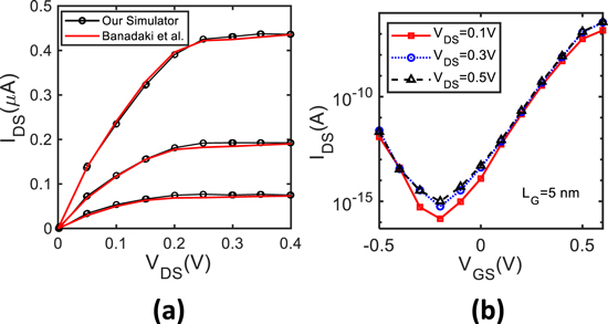
Figure 3. (a) Output characteristics of the simulated GNRFET calibrated against the results reported by Banadaki et al. 12 (b) transfer characteristics of the simulated GNRFET for different drain bias at LG = 5 nm.
Download figure:
Standard image High-resolution imageImpact of gate dielectric material
High-k gate dielectric material reduces leakage current and improves electrostatic control of the gate terminal in aggressively scaled devices. However, their influence on device performance depends on the transport mechanism, 30 gate structure, 31 device dimensions 32 and channel material 33 of the transistor. In our model, the dielectric constant, k is varied between 3.9 (SiO2) to 24 (HfO2) which correspond to the commonly found dielectrics with lowest and the highest k-value, respectively. 34,35 With high-k dielectrics, enhanced vertical field across the gate oxide increases both the inversion charge density and the drain current in GNRFET while maintaining lower off-state current due to the increased control of thermal emission, which results in improved IOn /IOff ratio. However, as LG is scaled, the lateral electric field across source-drain grows stronger. Figure 4a shows that, as k changes from 3.9 to 24, the improvements in IOn /IOff ratio decrease from ∼20 × to ∼10 × when LG is scaled from 10 nm to 5 nm.
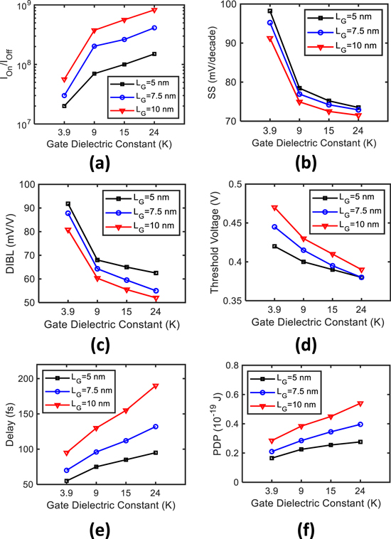
Figure 4. Effect of gate dielectric constant on (a) IOn /IOff ratio (b) subthreshold swing (c) DIBL (d) threshold voltage (e) gate delay and (f) power-delay product (PDP) for GNRFET with LG = 5, 7.5 and 10 nm. S/D doping concentration was taken as 0.01 per carbon atom (1%).
Download figure:
Standard image High-resolution imageEnhanced electrostatic control with increasing k, results in ∼25% improvement of SS and ∼35% reduction of DIBL as shown in Figs. 4b and 4c respectively, regardless of channel length scaling. On the other hand, VT in Fig. 4d decreases with increasing k because of further control of barrier height at the source end. With increasing k, VT changes from 80 mV at LG = 10 nm to 44 mV at LG = 5 nm. In Figs. 4e–4f, it is clear that both gate delay and PDP increase for high-k dielectric due to increased gate capacitance and higher values of (Qon - Qoff ) stemming from stronger gate control and increased inversion charge. As explained before, with the downscaling of LG , the increasing lateral field starts to weaken the benefits of increased vertical electric field. Thus, as shown in Figs. 4d–4f, the curve for LG = 10 nm has the highest slope and it gradually gets flatter as the channel length is reduced, indicating reduced gate control for shorter channels. Similarly, the increase in delay and PDP, due to the increase in k drops from 92% to 61% and from 100% to 40% respectively, when LG decreases from 10 nm to 5 nm. Table I reports the obtained values of performance metrics for different values of k.
Table I. Extracted values of performance metrics for different values of gate dielectric constant (k) at different LG .
| LG | k | IOn /IOff | SS (mV/decade) | DIBL (mV/V) | VT (V) | Delay (fs) | PDP (10−19J) |
|---|---|---|---|---|---|---|---|
| 5 nm | 3.9 | 2 × 10⁷ | 98.7 | 91.4 | 0.42 | 56 | 0.19 |
| 9 | 7.1 × 10⁷ | 79.0 | 66.9 | 0.40 | 79 | 0.22 | |
| 15 | 1.1 × 10⁸ | 75.1 | 64.0 | 0.39 | 84 | 0.23 | |
| 24 | 1.8 × 10⁸ | 73.0 | 62.0 | 0.38 | 92 | 0.27 | |
| 7.5 nm | 3.9 | 3.1 × 10⁷ | 95.2 | 88.0 | 0.44 | 68 | 0.20 |
| 9 | 2.1 × 10⁸ | 77.0 | 64.3 | 0.42 | 94 | 0.28 | |
| 15 | 2.6 × 10⁸ | 74.1 | 59.5 | 0.40 | 110 | 0.34 | |
| 24 | 4.1 × 10⁸ | 72.5 | 55.0 | 0.38 | 131 | 0.39 | |
| 10 nm | 3.9 | 4.7 × 10⁷ | 92.2 | 81.0 | 0.47 | 97 | 0.28 |
| 9 | 3.8 × 10⁸ | 74.5 | 60.3 | 0.43 | 129 | 0.39 | |
| 15 | 5.9 × 10⁸ | 72.3 | 55.4 | 0.41 | 154 | 0.46 | |
| 24 | 8.9 × 10⁸ | 70.6 | 51.8 | 0.39 | 187 | 0.56 |
Impact of source-drain doping
The effect of NS/D on the characteristics of GNRFET is analyzed by varying the concentration from 0.5% to 2% (2.5 × 10¹³ to 1014 cm−2). The band bending and the resultant energy barrier at source-channel (or drain-channel) junction, due to the S/D doping concentration, is given as:
With increased doping, the band bending in the junction increases, which draws the valence and conduction band closer at the off state operation for higher doping concentration, thereby increasing BTBT. 36 This can further be explained by the band-to-band Klein-Zener tunneling probability 37 from the source/drain reservoir to channel given by:
where  is the tunneling probability,
  is the reduced Planck's constant,
  is the longitudinal component of the wave vector in question and
  is the electric field present at the potential barrier at the S/D to channel interface given by,
  where,
  is the built-in voltage across the source/drain barrier and
  is the effective depletion width. Increasing the doping concentration results in rise of the barrier potential at the off state, thereby increasing the electric field which, in turn, increases the tunneling resulting in higher IOff
. IOn
also increases with increasing doping concentration due to the availability of higher amount of carriers for thermionic emission at any given temperature. However, the increase in IOff
dominates due to the exponential dependence of BTBT, causing degradation of IOn
/IOff
ratio for higher doping concentration, as shown in Fig. 5a. As channel length is scaled, it experiences stronger electric field,
is the effective depletion width. Increasing the doping concentration results in rise of the barrier potential at the off state, thereby increasing the electric field which, in turn, increases the tunneling resulting in higher IOff
. IOn
also increases with increasing doping concentration due to the availability of higher amount of carriers for thermionic emission at any given temperature. However, the increase in IOff
dominates due to the exponential dependence of BTBT, causing degradation of IOn
/IOff
ratio for higher doping concentration, as shown in Fig. 5a. As channel length is scaled, it experiences stronger electric field,  causing an increase in BTBT that accounts for 10 × decline in IOn
/IOff
ratio for LG
= 5 nm, whereas, the reduction in IOn
/IOff
ratio amounts to 2 × and 4 × for LG
= 10 nm and LG
= 7.5 nm respectively, as shown in Fig. 5a. Consequently, SS and DIBL also degrade for increasing doping concentration following the same trend, as illustrated in Figs. 5b and 5c respectively.
causing an increase in BTBT that accounts for 10 × decline in IOn
/IOff
ratio for LG
= 5 nm, whereas, the reduction in IOn
/IOff
ratio amounts to 2 × and 4 × for LG
= 10 nm and LG
= 7.5 nm respectively, as shown in Fig. 5a. Consequently, SS and DIBL also degrade for increasing doping concentration following the same trend, as illustrated in Figs. 5b and 5c respectively.
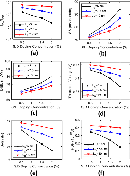
Figure 5. Effect of source-drain doping concentration on (a) IOn /IOff ratio (b) subthreshold swing (c) DIBL (d) threshold voltage (e) gate delay and (f) power-delay product (PDP) for GNRFET with LG = 5, 7.5 and 10 nm. Dielectric constant of k = 9 was considered.
Download figure:
Standard image High-resolution imageIncreasing NS/D causes further penetration of the depletion region into the channel region, causing a decrease in VT . This becomes more evident at shorter channel, which accounts for the steeper slope as channel length is scaled down. In Fig. 5d, VT is shown as a function of NS/D and its variation increases from 23 mV to 60 mV for LG = 10 nm and 5 nm respectively.
Because of increased leakage current, the off-state charge in the channel (Qoff ) increases with increasing NS/D , which causes both gate delay, τ = (Qon -Qoff )/Ion and PDP =(Qon -Qoff )VDD to decrease. With shorter LG , Qoff increases even more due to increased BTBT, which explains the steeper slope of the delay and PDP curve for shorter LG in Figs. 5e and 5f. For instance, at LG = 10 nm, the reduction in delay and PDP with increasing NS/D are ∼12% and ∼9% respectively, while for LG = 5 nm, this reduction is more pronounced (∼60% and ∼52%, respectively). Extracted values of aforementioned device characterestics are summarized in Table II.
Table II. Extracted values of performance metrics for different values of source-drain doping concentration (NS/D ) at different LG .
| LG | NS/D (%) | IOn /IOff | SS (mV/decade) | DIBL (mV/V) | VT (V) | Delay (fs) | PDP (10–19J) |
|---|---|---|---|---|---|---|---|
| 5 nm | 0.5 | 1.8 × 10⁸ | 74.3 | 62.0 | 0.43 | 110 | 0.33 |
| 1.0 | 7.4 × 10⁷ | 79.0 | 66.5 | 0.41 | 80 | 0.29 | |
| 1.5 | 4.9 × 10⁷ | 84.5 | 72.2 | 0.39 | 61 | 0.235 | |
| 2.0 | 1.9 × 10⁷ | 94.0 | 80.0 | 0.37 | 42 | 0.16 | |
| 7.5 nm | 0.5 | 3.9 × 10⁸ | 72.5 | 60.5 | 0.44 | 124 | 0.37 |
| 1.0 | 2.9 × 10⁸ | 76.4 | 63.2 | 0.43 | 112 | 0.36 | |
| 1.5 | 1.8 × 10⁸ | 80.0 | 67.1 | 0.42 | 100 | 0.343 | |
| 2.0 | 1.1 × 10⁸ | 87.0 | 73.0 | 0.41 | 85 | 0.32 | |
| 10 nm | 0.5 | 6.7 × 10⁸ | 71.5 | 58.0 | 0.45 | 140 | 0.43 |
| 1.0 | 5.9 × 10⁸ | 75.0 | 61.1 | 0.44 | 135 | 0.42 | |
| 1.5 | 4.5 × 10⁸ | 76.8 | 64.3 | 0.44 | 127 | 0.405 | |
| 2.0 | 3.7 × 10⁸ | 81.0 | 68.0 | 0.43 | 123 | 0.395 |
Impact of temperature
Although graphene shows superior thermal conductivity compared to its peers, being inherently 2D material, the performance of graphene devices depends on the thermal properties of the oxide and the substrate on which the graphene channel is fabricated. 38 A rise in temperature of around 200 K has been linked with instability in graphene devices through experimental studies. 39 Increasing temperature causes enhanced thermal emission, which increases the current in both ON and OFF state. But leakage current increases more compared to IOn as more carriers can hop over the barrier at higher temperatures. Thus, IOn /IOff degrades with increasing temperature as shown in Fig. 6a. For a rise of temperature ΔT = 150 K, highest degradation of 52% occurs for LG = 5 nm and lowest degradation of 19% occurs for LG = 10 nm.
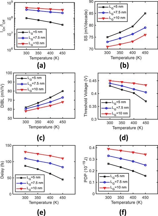
Figure 6. Effect of temperature on (a) IOn /IOff ratio (b) subthreshold swing (c) DIBL (d) threshold voltage (e) gate delay and (f) power-delay product (PDP) for GNRFET with LG = 5, 7.5 and 10 nm. NS/D = 1% and k = 9 was assumed.
Download figure:
Standard image High-resolution imageAs shown in Fig. 6b, for ΔT = 100 K, 12% degradation of SS is observed for GNRFET with LG = 10 nm, compared to 48% degradation reported for Si FinFET with LG = 15 nm. 40 The VT variation with temperature in GNRFET is 0.41 mV/°C, against ∼0.9 mV/°C for Si FinFET. 41 In parallel, gate delay and PDP is also reduced by a margin of ∼13% and ∼15% respectively, for ΔT = 100 K, regardless of LG due to increase in both Qoff and Ion , as shown in Figs. 6e–6f. Thus, on the whole, GNRFET showed more robust behavior against temperature variation than conventional Si devices. Table III shows the extracted values of performance metrics of GNRFET at different temperature.
Table III. Extracted values of performance metrics for different temperature (T) at different LG .
| LG | Temperature (T) | IOn /IOff | SS (mV/decade) | DIBL (mV/V) | VT (V) | Delay (fs) | PDP (10–19J) |
|---|---|---|---|---|---|---|---|
| 5 nm | 300 | 9.6 × 10⁷ | 75.4 | 64.1 | 0.43 | 85 | 0.26 |
| 350 | 6.8 × 10⁷ | 77.6 | 68.0 | 0.41 | 77 | 0.23 | |
| 400 | 5.2 × 10⁷ | 79.4 | 74.1 | 0.40 | 69 | 0.20 | |
| 450 | 4.3 × 10⁷ | 85.1 | 80.2 | 0.37 | 46 | 0.16 | |
| 7.5 nm | 300 | 4.4 × 10⁸ | 73.1 | 60.7 | 0.44 | 110 | 0.33 |
| 350 | 4.1 × 10⁸ | 74.7 | 64.3 | 0.43 | 102 | 0.30 | |
| 400 | 3.7 × 10⁸ | 76.2 | 68.1 | 0.41 | 95 | 0.28 | |
| 450 | 3.3 × 10⁸ | 78.8 | 73.2 | 0.40 | 83 | 0.25 | |
| 10 nm | 300 | 3.3 × 10⁸ | 71.4 | 58.2 | 0.45 | 135 | 0.40 |
| 350 | 2.9 × 10⁸ | 72.2 | 61.3 | 0.44 | 126 | 0.38 | |
| 400 | 2.6 × 10⁸ | 73.2 | 64.1 | 0.44 | 117 | 0.35 | |
| 450 | 2.5 × 10⁸ | 76.2 | 68.2 | 0.43 | 110 | 0.32 |
Impact of channel length scaling
To determine the performance of GNRFETs with scaling, LG was varied from 10 nm to 2.5 nm while tox was fixed at 1.5 nm, thus keeping the vertical field constant. Figure 7a shows the transfer characteristics for different LG , where both IOn and IOff are increasing with decreasing LG due to increased thermionic emission. However, since BTBT increases exponentially with decreasing LG , off-current increases significantly, leading to a notable degradation in IOn /IOff ratio for shorter LG , as shown in Fig. 7b. For instance, ∼3 × degradation in IOn /IOff ratio is observed when LG decreases from 7.5 nm to 5 nm, while ∼12 × decline is obtained for a decrease in LG from 5 nm to 2.5 nm. Similarly, VT , SS and DIBL also degrades with decreasing LG , where a substantial degradation is observed below LG = 5 nm as illustrated in Fig. 7c. In common with Si devices, 42 LG scaling leads to decreased gate capacitance in GNRFET, resulting in reduced gate delay and PDP with decreasing LG , as shown in Fig. 7d.
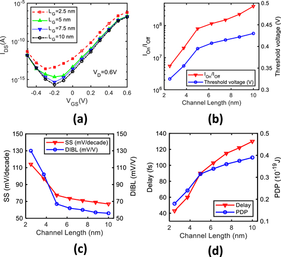
Figure 7. (a) Transfer characteristics, (b) IOn /IOff ratio and threshold voltage, (c) subthreshold swing and DIBL, (d) gate delay and power-delay product for varying channel length. NS/D = 1% and k = 9 was considered.
Download figure:
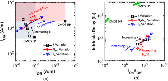
Standard image High-resolution imageBenchmarking GNRFET with CMOS LP and HP criteria
Based on the IRDS metrics, 29 we compare the performance of our simulated GNRFET with the LP and HP CMOS devices in the 5 nm technology node. Figure 8a shows the range of IOn and IOff subjected to variation of different device parameters, where the shaded areas are the targeted regions for LP and HP operation. All data points presented here were extracted from our simulations at LG = 5 nm (except for LG variation) at operating voltage of VDD = 0.65 V. Due to higher bandgap of 1.53 eV, compared to 1.12 eV in conventional Si based logic devices, (7, 0) AGNR assists suppression of leakage current in the off-state, which allows GNRFET to maintain LP performance over a wider range of variations in the device parameters. In fact all the parameter variation ranges tested in Figs. 4–6, satisfy the LP criteria. However, HP design criteria can only be met with higher end of source/drain doping and dielectric constant. At LG = 2.5 nm, the leakage current increases significantly beyond the IOff requirement of LP design and therefore, the GNRFET loses the design freedom for optimized energy efficient circuits.
Figure 8. (a) IOn and IOff map with shaded regions showing CMOS HP and LP criteria by IRDS for the 5 nm node. 29 (b) intrinsic delay time vs IOn /IOff ratio; simulation results for the GNRFET is compared with the CMOS HP and LP criteria by IRDS for the 5 nm node.
Download figure:
Standard image High-resolution image
Power-performance optimization in GNRFET is directly related to the speed and energy consumption of the FET switch. 43 In Fig. 8b, GNRFET is evaluated considering intrinsic gate delay vs IOn /IOff ratio. The delay and IOn /IOff ratio from the literature, that meet the HP and LP requirements set by IRDS, are shown in Fig. 8b, along with the extracted values from our simulations. 29,44 The comparison shows that GNRFET can achieve both HP and LP design criteria in terms of both gate delay and IOn /IOff ratio. However, higher IOn /IOff is achieved at the expense of higher gate delay in all cases. For this reason, the design target is to keep the slopes of Fig. 8b, as low as possible. This allows attaining better IOn /IOff ratio without significantly compromising gate delay. This is best achieved with utilization of high-k dielectric materials, while a notably fast switching can also be achieved with higher source/ drain doping concentration and channel length scaling.
Conclusions
In this paper, an extensive quantitative analysis, on key performance metrics of a double gated GNRFET, has been performed under a single simulation platform. High accuracy of the model was ensured by implementing TB band structure calculation of GNR which is verified by DFT calculation. Quantum transport simulations were self-consistently performed with electrostatics using energy-position dependent effective mass Hamiltonian. The impact of various device parameters on the performance of the GNRFET, with respect to channel length scaling, were investigated. The study revealed that improvement in device speed, with high-k dielectrics, drops ∼33% when LG decreases from 10 nm to 5 nm. On the other hand, over 2 × faster switching speed and ∼80% higher drive current can be achieved by increasing source/drain doping from 0.005 to 0.02 molar fractions, while compromising the IOn /IOff ratio by an order of magnitude. The GNRFET also showed less variation in performance with ambient temperature changes when compared to Si devices. Immunity to short channel effects was also observed for GNRFET above 5 nm. Finally, benchmarking with the IRDS design specifications suggested that higher source/drain doping concentrations and high-k dielectric expedite designs for high-speed applications, while for LP applications, low to moderate doping works appreciably well. These extensive and systematic analyses will provide useful insights for the design and performance optimization of GNRFET based circuits and systems.