
Abstract
The microstructural changes and degradation under forward bias of vertical β-Ga2O3 rectifiers were observed by in-situ transmission electron microscopy. The devices show both a voltage dependence for the onset of visible degradation as well as a time dependence at this threshold voltage, suggesting a defect percolation process is occurring. The degraded rectifiers show a large decrease in forward current and different types of crystal defects are present, including stacking fault tetrahedra, microcracks, Ga-rich droplets and Au inclusions from the top electrode. Continued forward bias stressing is known to lead to macro-cracks oriented along the [010] crystal orientation and eventual delamination of the epitaxial drift layer, but this study is the first to provide insight into the appearance of the smaller defects that precede the large scale mechanical failure of the rectifiers. The initial stages of bias stressing also produce an increase in deep trap states near EC−1.2 eV.
Export citation and abstract BibTeX RIS
β-Ga2O3 is attracting considerable attention for high power electronics with low switching losses.1–10 The wide bandgap (∼4.8 eV), demonstrated breakdown field of >5 MV. cm−1 1 and availability of large area, relatively inexpensive substrates suggests this material may play a role in future power conditioning systems,11–25 providing SiC-like performance at near Si -like cost.26,27 The absence of provable p-type doping limits the technological applications of this material to unipolar devices such as rectifiers and MOSFETs.4–25 While both enhancement- and depletion-mode lateral and vertical MOSFETs have been demonstrated,4–12,14 the most promising early technology insertion point appears to be vertical geometry rectifiers.13,15–25 Breakdown voltages of 2.9 kV have been achieved in trench design vertical rectifiers23 and 2.3 kV in field-plated planar vertical designs,16 the latter with high current. When driven to failure under high reverse bias voltages, the devices breakdown at the contact periphery,28 indicating that the edge termination designs are still not optimized. Under high forward current densities, post-mortem studies show cracking of the Schottky contact region along preferred orientations and eventually delamination of the epitaxial drift layer from the underlying conducting substrate.18 However, the initial stages of rectifier degradation have not yet been captured.
In this paper, we report on real-time, in-situ studies of vertical rectifier failure under forward bias conditions using electron transparent functional devices operated within a transmission electron microscope. This allows observation of the microstructural and chemical changes occurring in the drift region under high forward current density conditions. Electrical measurements also show an increase in deep trap states in the early stages of degradation.
Experimental
The epitaxial layer structure and rectifier fabrication have been described elsewhere.16–19 Edge termination consisted of a bilayer field plate and the vertical Schottky diodes were fabricated on a 20-μm thick Si-doped n-type (∼1016 cm−3) Ga2O3 drift layer grown on 650-μm thick β-Ga2O3 substrate using halide vapor phase epitaxy (HVPE). The β-Ga2O3 substrate was a Sn-doped Ga2O3 single crystal wafer with (001) orientation grown by the edge-defined film-fed method with a carrier concentration of 3.6 × 1018 cm−3. A full-area backside Ohmic contact was formed with electron beam deposited Ti/Au, followed by rapid thermal annealing at 550 °C for 30 s in N2. Next, 40 nm of SiO2 and 360 nm of SiNx were deposited as the field plate dielectric layers. The dielectric contact windows (0.2 mm diameter circles) were opened using 1:10 diluted buffered oxide etchant (BOE). E-beam evaporated Ni/Au (80/420 nm) metallization was used for the Schottky contacts, which overlapped the dielectric windows by 10 μm. Figure 1 shows a schematic of the completed device.
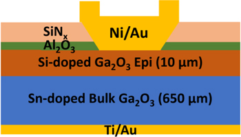
Figure 1. Cross-sectional schematic of initial rectifier. After device measurements are performed, this is sectioned into lamellae for in-situ biasing.
Download figure:
Standard image High-resolution imageDeep Level Transient Spectroscopy (DLTS) was performed on the as-fabricated rectifiers, which were 800 μm square, as well as after bias stressing under forward bias at 1 V forward bias for 5 min to produce a reduction in breakdown voltage from 600 V to 20 V. The purpose was to observe changes in defect spectra in the early stages of degradation before complete failure of the device.
Electron transparent (∼100 nm thick) β-Ga2O3 coupons were prepared and lifted out from the completed rectifiers using a Ga+ Focused Ion Beam (FIB) in a Helios Nanolab DualBeamTM scanning electron microscope.29–31 This process involved wire bonding of the micro-electromechanical system (MEMS) device on a TEM chip carrier and transfer of the sample onto this MEMS device.29,30 At first, a coupon was lifted out from the bulk β-Ga2O3 rectifiers and attached on a copper TEM grid, which was further thinned down to a 100 nm thick electron transparent state using the Ga+ FIB. Thinning down of the coupon involves a series of ion beam accelerating voltages and a wide range of current steps from 21nA–72pA. The thickness of the sample was monitored at regular intervals during the thinning process, and both accelerating voltage and currents were adjusted depending on the sample thickness. Then the sample was transferred from the TEM copper grid to the MEMS device and then mounted on an in-situ TEM holder. Electrical characterization was performed inside a field emission 200 kV FEI Talos F200X TEM equipped with energy dispersive spectroscopy (EDS) with 1.2 Å resolution. The purpose of these experiments was to observe the time dependence of changes in crystallinity and extended defects as the device were driven to failure. We examined three different coupons.
Results and Discussion
The rectifiers were examined by TEM for the presence of defects in the as-fabricated devices prior to any biasing. Figures 2 and 3 show cross-sectional images of the rectifiers, in which a variety of defects are observed. These include threading dislocations, rod-shaped defects common to β-Ga2O3 and stacking faults.32–44 The high resolution image does not reveal the presence of any divacancy-interstitial complexes that have been reported in Sn-doped bulk Ga2O3.45 Previous work has also identified extended defects (e.g., twin boundaries and screw dislocations)32,33 and some atomic-scale defects in bulk and epitaxial Ga2O3.34,35 However, as will be seen below, once the rectifiers are biased, new defects appear. We observed quantitatively similar results for all coupons tested, although for consistency, we show all the images from one device since we had a complete set of images for this and for the others we had less complete data.

Figure 2. TEM cross sectional views of rectifier prior to forward bias stressing, showing presence of extended defects.
Download figure:
Standard image High-resolution image
Figure 3. TEM cross sectional images taken near the top Au contact prior to bias stressing, showing stacking faults.
Download figure:
Standard image High-resolution imageThe 100 nm electron transparent β-Ga2O3 rectifiers were tested under accelerated forward biasing conditions, in which the forward bias was increased in intervals of 20 mV until device failure occurred at 0.48 MV cm−1 (4.81 V). Each biasing step was followed by a one minute delay for relaxation. Figure 4a shows the current-voltage (I-V) characteristics under forward biasing conditions, with the Schottky contact at various forward biases and the substrate grounded. Figures 4b–4g shows the low magnification TEM bright field images to capture microstructural changes during the forward biasing at the different bias points labelled in Fig. 4a. Up to 2.25 V forward bias, no microstructural changes were observed. We also did not observe any abrupt changes in the I-V characteristics below this bias. The calculated current density at this point is approximately  This current density is sufficient enough to introduce thermal stress35,36 in the sample which could further initiate microstructural changes, as shown by pink color dotted rectangular box and cyan color dotted circle in Fig. 4c. As the forward bias is increased to 2.45 V (corresponding I-V characteristic is indicated by point (d) on Fig. 4a), a change in the slope of the I-V characteristic is evident. This slope change signals the onset of crystal defect generation due to the high current density (3.24 × 10⁴ A.cm−2), which further increases the series resistance of the sample.33–35

Figure 4. (a) I-V characteristics under forward biasing condition; TEM bright field images at different biasing voltages: (b) 0 V, (c) 2.25 V, (d) 2.45 V, (e) 2.61 V, (f) 4.35 V, and (g) 4.81 V.
Download figure:
Standard image High-resolution imagePoints (d) to (e) in Fig. 4 show an abrupt and sharp current density increment from 2.45 V to 2.61 V. This behavior may be explained by increased defect generation rate due to heating and increased carrier energy. At high forward biases, carriers gain sufficiently high energy, and both barrier potential and bandgap are reduced37 which could counter-balance the rate of defect generation at this moderate current density (compared to the breakdown current density). Beyond 2.61 V, the current density is high enough to introduce more defects in the device, which is even visible at low magnification, as shown in Fig. 4f. The increase of bias from 2.61 to 4.35 V(points (e) to (f) on Fig. 3a) clearly indicates an additional change in slope of the I-V curve, which could be attributed to the more pronounced effect of carrier traps and series resistance in the device. At 4.35 V forward bias current density is  which could induce sufficiently high thermal stress and micro-structural defects due to the moderate thermal conductivity of Ga2O3. This is reflected by point (f) in Fig. 4a where current drops sharply. After 4.35 V forward bias, the output current value slightly increased as marked by point (g) on Fig. 2a. However, series resistance at this point is a maximum during forward biasing. At 4.81 V, current density is more than two orders of magnitude higher than the reported21,34 threshold value for failure, and current drops, as shown in Fig. 4a. At this stage current density is high enough to introduce structural degradation due to the thermomechanical field, as shown by pink color dotted rectangular box and cyan color dotted circle in Fig. 4g.
For clarity, Fig. 5 shows a side-by-side cross-sectional comparison of the rectifier before (left) and after (right) biasing to 4.7 V, where the current shows the device has significantly degraded. Note the appearance of extended defects near both the anode and cathode, as well as a degradation of the selected area diffraction pattern.

Figure 5. Cross sectional images and SAED patterns from rectifier before and after bias stressing at 4.7 V to induce degradation.
Download figure:
Standard image High-resolution imageHigh resolution images taken in the center of the epitaxial layer for different forward biases are shown in Fig. 6. The pristine crystal quality prior to bias application is evident in the 0 V image. However, various degrees of lattice disorder become apparent as the bias is increased up to 4.8 V. Note that changes are already obvious at 2.45 V (current density of 3.24 × 10⁴ A.cm−2). This correlates with electrical measurements, which shows that irreversible damage to the rectifiers occurs for temperatures in the drift region above ∼ 270 °C and at temperatures above 350 °C the Au-based metallization fails.38

Figure 6. Higher resolution cross-sectional images as a function of forward bias on the rectifiers, showing the change in crystal quality.
Download figure:
Standard image High-resolution imageA more detailed view of the spatial variation in defect introduction is shown in Figs. 7 and 8, which show cross-sectional images take from near the cathode (Fig. 6) and anode (Fig. 7), respectively, as a function of forward bias. Near the cathode (Ti/Au contact), the appearance of defect clusters are apparent as the bias increases until the appearance of an extended defect at the failure point. A similar trend is obvious near the Au anode, where defects with size ∼100 nm appear at the failure point. We subsequently performed EDS to gain insight into the chemical composition of these defects. It is also worth noting that the diffraction patterns at the failure point, even away from the extended defects, showed significant changes. Figure 9 shows diffraction patterns taken at three different locations near the top of the rectifier structure where the heating during forward biasing will be most severe. There is even an indication of a change in zone axis in this region.

Figure 7. Cross-sectional images near the Ti/Au cathode, as a function of forward bias during electrical stressing.
Download figure:
Standard image High-resolution image
Figure 8. Cross-sectional images near the Ni/Au cathode, as a function of forward bias before and after electrical stressing at 4.81 V.
Download figure:
Standard image High-resolution image
Figure 9. SAED from three regions near the top Ni/Au contact after forward bias stressing at 4.81 V.
Download figure:
Standard image High-resolution imageA time series analysis of the sample at 4.81 V prior to the failure is shown in Fig. 10. This provides an insight on how and where the degradation starts and propagates inside the rectifier. The green and cyan color arrows indicate regions near the anode and cathode electrode, respectively, whereas pink color arrow indicates the direction of gradual migration and evaporation. In Figs. 10a–10d, both green and cyan color dotted arrow show contrast change near the cathode, indicating microstructural changes under high current density, which further degrades after 15.5 s biasing time at 4.81 V. Pink color arrow indicates the direction of gradual contrast change with experiment time. This contrast change could be attributed to the evaporation/migration of atoms from cathode to anode side under very high current density i.e. 1.65 × 10⁵ A cm−2. Due to the low thermal conductivity of Ga2O3 and applied high forward current density, metal pools that are Au or Ga -rich can form in the drift layer39 as captured by scanning transmission electron microscope (STEM) image in Fig. 10f and confirmed by the EDS scans. The formation of Au- or Ga-rich metal particles might also result from surface diffusion of the respective elements on the surface of the thin TEM sample. At this point, we can't confirm the mechanism.

Figure 10. Time series TEM BF images of defects evolution prior to the failure at 4.81 V: (a) 0 s, (b) 5 s, (c) 10 s, (d) 14 s, (e) 15.5 s, and (f) HAADF STEM image after failure.
Download figure:
Standard image High-resolution imageAt very high current density (bias of 4.81 V, current density 1.25 × 10⁵ A.cm−2), the rectifier is seen to undergoes severe lattice damage and degradation, as shown in Fig. 11. The extent of the degradation during the high forward biasing could be understood using selected area electron diffraction (SAED) patterns. Such a SAED pattern is shown in Fig. 11b. Appearance of a ring (as indicated by yellow color dotted arrow) in SAED pattern clearly indicates the device has undergone severe lattice damage. This observation is supported by Figs. 11c–11f where lattice damage and defects are evident. Figure 11g shows different types of defects, including multiple stacking fault tetrahedrons (SFT) which could be an outcome of thermal stress, and Fig. 11f shows an individual stacking fault tetrahedron at high resolution. SFT defects are obvious indicators of vacancy generation in the rectifier drift layer under high current density. These vacancies further accumulate to form SFT defects as shown in Figs. 11e and 11f. Similar types of stacking fault defects in Ga2O3 has been reported recently.32–35

Figure 11. (a) Low magnification TEM BF images after failure i.e. at 4.81 V, (b) SAED pattern after failure, (c)–(d) magnified view close to the center area as shown by pink color dotted rectangle, (e) HRTEM images showing SFT defects in a defected region of the sample, and (f) HRTEM images of an individual SFT defect.
Download figure:
Standard image High-resolution imageIt is known from proton irradiation studies that the dominant center in β-Ga2O3 is a VGa(1)–2H complex.40,41 Electron Paramagnetic Resonance of radiation damage centers in β-Ga2O3 has identified a VGa(1) center with a structure very similar to this VGa(1)–2H complex except with two bound holes instead of two hydrogen atoms.42–44 This type of structure has also been observed using scanning transmission electron microscopy.45 Thus it appears that VGa complexes form, probably due to the high thermal load in the epitaxial layer and these agglomerate into different types of extended defects that are observed in the TEM and which are the signatures of the impending failure of the rectifier.
β-Ga2O3 rectifiers can suffer generation of generate cracks and defects at electrodes as well as in the device layer under forward biasing conditions.18,36,38 Figure 12 illustrates such defect evolution in the drift layer during the forward biasing. Additional extended defects observed as the forward bias was increased included voids and microcracks. We did not notice any crystal defects before forward biasing, as shown in Fig. 12a. Beyond the threshold current density of 2.24 × 10⁴ A cm−2, minor crystal defects starts to arise, as indicated by the circular regions in Fig. 12b. These defects are more evident at 6.69 × 10⁴ A cm−2 as shown in Fig. 12c. Figure 12d shows a magnified view of Fig. 12c, where both extended defects and clusters are evident. These defects near the anode could affect Schottky barrier height at the interface,37 which would further affect forward output current. Above 2.61 V forward biasing, which corresponds to 6.69 × 10⁴ A cm−2, thermal stress induces a significant amount of crystal defects, which further reduce forward current. This is supported by the corresponding I-V characteristic, which showed an increase in sheet resistance. With increased forward bias voltage, the rectifier failure is accompanied by formation of vacancy enriched areas, as indicated in Figs. 12 d and 12e. We also noticed a disruption in crystal structure and formation of small crystallites. This indicates the single crystal Ga2O3 disintegrates to a polycrystalline structure, which significantly affect the device performance. These defects act as carrier traps and might increase series resistance of the rectifiers. Thus, defects induced series resistance increment further degrades forward output current. During the failure both metal pool (green color dotted circle) and discernable cracks (pink color dotted rectangle) formed in the device layer near the cathode as shown in Figs. 12e and 12f. A magnified view of the crack is shown in Fig. 12f. This current density is higher than the reported breakdown value, which could induce sufficient amount of thermal stress in the device layer and initiate mechanical cracking.21,34 The formation of pores and cracks could also be related to surface diffusion and bending of the thin TEM lamellae, although as discussed earlier, the lamellae behave in a similar fashion to the large area, ex-situ devices.

Figure 12. Defect evolution during the forward biasing at: (a) 0 V, (b) 2.25 V, (c) 2.61 V, (d) magnified view at 2.61 V, and (e) HAADF image at 4.81 V, and (f) TEM BF image at 4.81 V.
Download figure:
Standard image High-resolution imageLet's address the possible influence of the probe beam in the TEM affecting the results. It might be suggested that β-Ga2O3 is a very beam-sensitive material and many of the effects observed could also be caused by radiation damage. In particular, the SFT defects observed in the HRTEM images and the breakdown into nanocrystalline particles could also be indicative of an agglomeration of point defects caused by the electron beam. However, under our beam conditions, we have not seen any obvious creation of stacking faults, transformation into nanocrystallites or agglomeration of point defects. The lamellae behave the same as large area devices under similar current densities. While there are potential issues under electron beam irradiation, but we haven't seen them under our conditions. The TEM sample preparation was done to minimize the total beam energy density. Similarly, while some of the changes may be due to thermally induced effects caused by Joule heating of the sample and not to the forward bias current induced effects, we have spent a lot of time quantifying the effects of Joule heating under forward bias in the original diodes from which the lamellae for TEM were cut and we feel we have a good handle on how that is manifested. That's not what we are seeing in the devices biased in the TEM. The changes we see in these lamellae are basically similar to those seen in ex-situ devices where we maintain the temperature below the point of thermal failure.
Deep level transient spectroscopy measurements were used to observe any changes in deep traps as a result of the bias stressing. Ax shown in Fig. 13, the spectra in the as-fabricated rectifier shows the standard E1 (level near Ec−(0.57–0.63) eV, electron capture cross section of σn = (3.6–4.5)×10–14 cm2), E2 (level near Ec−0.83 eV, σn = 1.4 × 10⁻¹⁴ cm2) electron traps, shoulder belonging to the E2* trap, and, at high temperature, the trap similar to E4 trap in radiation experiments, but with slightly altered parameters (Ec−1.4 eV, σn = 6 × 10–12 cm2), trap E4*, observed in some HVPE films.46–49 The only solid identification of these traps is that E2 is due to the Fe3+/Fe2+ acceptor.46 The other states are thought to be point defect related.47–49 After degradation the spectra in the low temperature part were virtually unchanged, but the magnitude of the E4* peak greatly increased and the peak was converted to the standard radiation defect peak E4 (Ec-1.2 eV, σn = 1.1 × 1014 cm−2). The E4* peak is peculiar because we have also observed it being transformed by neutron irradiation into E4 and slightly anneal at temperatures higher than 450 oC. Since the E4 state is introduced by neutron, proton and alpha particle irradiation,47–49 it is expected to be related to native point defects or their complexes with impurities and its increase in bias-stressed samples may indicate the creation of these states provides percolation sites for the more extended defects found by TEM after higher bias stressing.

Figure 13. DLTS spectra measured before (red lines) and after (blue lines) degradation at −5V, with forward bias pulse +1 V (50 ms long), the data shown for time windows 150 ms/1500 ms (solid lines) and 1500 ms/15000 ms (dashed lines).
Download figure:
Standard image High-resolution image
Summary and Conclusions
This work demonstrates an in-situ technique to investigate accelerated failure of β-Ga2O3 rectifiers inside a TEM. There are a number of key points that emerge from this study:
- (i)During device operation, high current densities induce a significant concentration of crystal defects in the drift layer, which in turn increases series resistance and may increase carrier trapping.
- (ii)At high current density, the electrode metal can also degrade, thus introducing inhomogeneous Schottky contact at the metal-semiconductor interface.
- (iii)Metallic pool formation during the failure of the device indicates temperature plays a role in the rectifier breakdown.
- (iv)Reduction of Ga and O atom near the cathode area may be a result of the migration of atoms under high current density.
- (v)Very high current density can also generate cracks in the drift layer prior to the failure of the rectifier. This can eventually lead to delamination of this layer from the substrate.
The existing literature considers only post failure analysis to predict the failure modes, whereas the current study allows us to probe defects evolution and failure modes during real-time operation. This will also be interesting for looking at reverse bias degradation mechanisms, since recent results suggest near-ideal reverse leakage current and maximum electric field can be obtained in some existing material.50 Given our knowledge of the end result of forward bias degradation on large devices, in our observations, the lamellae end up with the same failure mechanisms. The TEM experiments allow us to see the evolution of that, rather than just the end result.50,51
Acknowledgments
The work at UF is partially supported by HDTRA1-17-1-0011 (Jacob Calkins, monitor), the DTRA Interaction of Ionizing Radiation with Matter University Research Alliance and also by NSF DMR 1856662 (James Edgar). The work at NUST MISiS was supported in part by the Russian Science Foundation, grant no. 19-19-00409 and grant К2А-2018-051 Ministry of Education and Science of the Russian Federation in the framework of Increase Competitiveness Program of NUST "MISIS" supporting Nastya Kochkova. Research at the NRL was supported by the Office of Naval Research (ONR).