
Abstract
In this study, we present a new method named seed-induced lateral crystallization (SILC), wherein the Ni that is deposited on amorphous silicon (a-Si) is removed prior to crystallization. The newly developed polycrystalline silicon (poly-Si) thin-film transistor (TFT) exhibits a field effect mobility of 63 cm2/V-s, leakage current of 7.9 × 10⁻¹¹ A, slope of 0.8 V/dec, Ion of 2.8 × 10⁻⁴ A at VD = 10 V, and VTH of 5.5 V. The leakage current has been reduced by an order of magnitude as compared with conventional metal-induced lateral crystallized (MILC) poly-Si TFTs, in which Ni is removed after the crystallization. In order to materials analysis, Raman scattering spectroscopy and field emission scanning electron microscopy (FESEM) was used. Since a batch process is possible in MILC technology, it is more advantageous than the excimer laser annealing (ELA) technology for mass production of a large size display. Since SILC TFT shows a leakage current comparable to an ELA poly-Si TFT, its application to the mass production of AMOLED display is expected have a substantial impact on the industry.
Export citation and abstract BibTeX RIS
Active matrix organic light emitting diode (AMOLED) technology has many advantages over liquid crystal display (LCD) in terms of display functions and is, therefore, beginning to replace LCD technology. Because AMOLED requires low-temperature polycrystalline silicon (poly-Si) thin-film transistors (TFTs), for which no industrial technology is yet known, very limited and only small size display is available so far. The excimer laser annealing (ELA) is a typical low-temperature crystallization method but suffers from two critical problems, which have not yet been overcome in terms of cost for mass production. One is the inevitable scan overlap, which leads to crystal non-uniformity; the other is the resulting surface roughness, which stems from a liquid-solid phase transformation.1
In order to meet the current demand, the development of a novel low-temperature polycrystalline silicon (LTPS) process that is suitable for mass production is imperative. Much research has been devoted to building high mobility TFTs for AMOLED, including microcrystalline Si,2 oxide semiconductors,3 and so on. More recently, a few experiments that attempt to compensate for some of the drawbacks of the ELA process have been reported. Some examples include sequential lateral solidification (SLS), a partial laser melting of silicon in vertical,4 and an ELA method combined with metal-induced lateral crystallization (MILC).5 However, some obvious problems still remain. Since amorphous silicon (a-Si) thickness is less than 1000 Å, achieving partial melting along the thickness would be very difficult. Also, once a laser has been used, it is not sensible to combine it with MILC for the sole purpose of reducing the crystallization temperature. Another reported process included gettering of Ni silicide with phosphorous-doped Si, but no promising results were obtained.6
Yoon and coworkers have discovered that when Ni is deposited on a part of a-Si, it forms a Ni silicide at temperatures as low as 300°C.7 Since the thickness of a-Si is typically less than 1000 Å, crystallization along the depth of silicon does not take much time. Lateral crystallization occurs by a catalytic phase transformation, during which a fragment of Ni silicide with thickness less than 50 Å moves toward a-Si, leaving behind the poly-Si. The term 'catalytic' is used because no diffusion of Ni is involved in this phase transformation. When a fragment of Ni silicide comes across the poly-Si crystallized by another fragment, it cannot move forward and is reflected in other directions where a-Si is available. After some reflections of this kind, Ni silicide becomes trapped at the grain boundaries where there is no more a-Si available in any direction. These trapped Ni silicides are responsible for the high leakage current, which is the main drawback of MILC TFTs8,9 – as well as for some other poor electrical properties, such as low mobility and low on-state current. Therefore, by reducing the amount of Ni trapped at the grain boundaries of poly-Si, it should be possible to greatly reduce the leakage current of MILC poly-Si TFTs. Until now, no one has reported the effective elimination of this defect.
In our earlier report, Ni was sputtered on a-Si thin film, heat-treatment was carried out for crystallization,10 and the Ni was removed by H2SO4. Although many researchers have attempted to determine the basic mechanism for the MILC phenomenon, it is not yet completely understood.11–14 In order to minimize the amount of trapped Ni silicide at the grain boundaries of the poly-Si, Ni was sputtered and then immediately removed. Ni was deposited on a-Si at room temperature, 100°C, 200°C, and 300°C. This process of lateral crystallization took a bit more time than the conventional MILC process, but poly-TFTs prepared in this manner showed much better electrical properties than MILC TFTs. This process is named "seed-induced lateral crystallization (SILC)" Because a seed must be formed right after sputtering of Ni in order to produce a lateral crystallization, even when the substrate is kept at room temperature during Ni sputtering.15 Systematic studies have been carried out to control the amount of Ni silicide at the channel of TFT and the relationship between the amount and location of Ni silicides along the channel; as a result, some interesting electrical properties of TFTs, especially a behavior of the leakage current, have been revealed. In general, the electrical properties of SILC TFTs were found to be comparable to those of laser-scanned poly-Si TFTs, thus indicating that they are suitable for application to AMOLED pixel fabrication. Since no scanning is required and a batch process is possible, SILC is much more advantageous over the ELA for use in mass production and large screens. Hence, we believe the SILC process can usher in a new era of AMOLED display.
Experimental
In this work, we present two sets of experiments – metal-induced crystallization (MIC) and seed-induced crystallization (SIC) groups. For both groups of experiment, Ni was sputtered onto a-Si thin film deposited on a common glass (Corning eagle XG, 105 × 105 mm2) by low-pressure chemical vapor deposition (LPCVD). The thickness of a-Si was 800 Å and that of Ni was approximately 50 Å. In the MIC process, Ni was not removed prior to crystallization; the substrate was heated at 550°C for 2 hours, and Ni was removed by H2SO4 after the crystallization was complete. In the SIC process, however, Ni was removed prior to the crystallization. Ni was sputtered at room temperature, as well as at different substrate temperatures, such as 100°C, 200°C, and 300°C; however, the room temperature samples showed the best electrical performance. In each group of experiments, three different methods of Ni sputtering were exercised: (1) Ni was blanket sputtered in MIC and SIC. (2) Ni was sputtered on a-Si after the formation of the gate in self-aligned MILC and SILC (hereinafter, referred to as SA-MILC and SA-SILC, respectively). (3) Ni was deposited about 4 μm away from each end of the gate by using an extra mask after gate formation and before Ni deposition in off-set MILC and SILC (hereinafter, OS-MILC and OS-SILC, respectively). Since Ni was deposited at both ends of the gate in a self aligned manner, (e.g., the gate performed as a mask even though Ni was blanket sputtered in this process) we expected to have a lot of Ni silicides at the space charge regions of the source, drain and channel. Of course, in SIC and MIC, Ni was deposited on the channel without any mask, so no lateral growth was expected. It is known that MIC TFTs cannot be used as pixel transistors due to poor electrical properties.8 Therefore, since n-channel TFTs usually showed worse electrical properties than p-channel TFTs in term of leakage current, only the latter were made in this experiment. ID-VG curves were measured with a Keithley 2636 system. Field effect mobility, threshold voltage, subthreshold slope, Ion, Ileak, and on/off ratio were calculated from the ID-VG measurement. The three different methods of Ni sputtering are illustrated for clear comparison in Fig. 1.
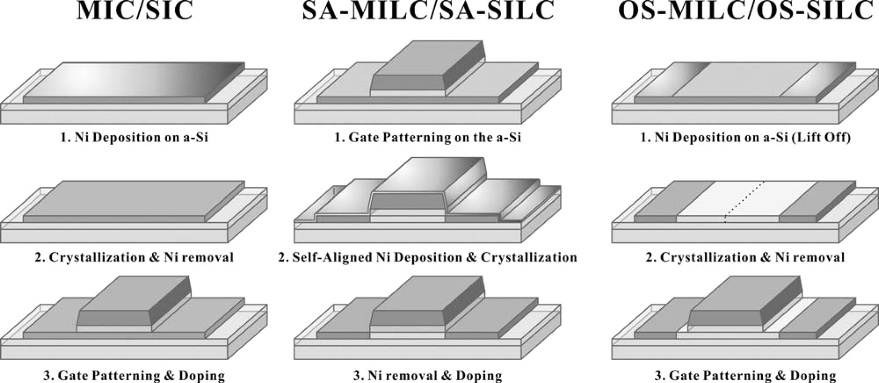
Figure 1. Schematic diagrams of poly-Si TFT cross-section views fabricated by (a) MIC/SIC, (b) SA-MILC/SA-SILC, and (c) OS-MILC/OS-SILC, respectively.
Results and Discussion
The leakage current behavior is well established in the previous studies,16,17 According to the studies, the leakage current is produced by two mechanisms as shown in Fig. 2. Two separated leakage current regions are appeared in the off-state region. Region A is first mechanism of leakage current which is thermionic emission due to thermal excitation of trapped carriers at relatively low gate voltages and high drain voltages. This leakage current mechanism is manifested by the "bump" and "minimum leakage current" in the ID-VG transfer curves. Region B is second mechanism of leakage current which is field emission due to field ionization of trapped carriers tunneling through the potential barrier and field-enhanced thermal excitation of trapped carriers at high reverse gate voltages. This leakage current mechanism is manifested by the "pinning" in the ID-VG transfer curves. The pinning means the increase of drain current that occurs with increasing gate voltage. The "pinning current" is defined as the maximum drain current in the high gate voltage region. The height of the bump and minimum leakage current in region A is related to the defects in the surface of the channel, and the pinning current is related to the amount of defects at the channel and drain junction, where the highest electric field is applied during the measurement. If the defect concentration in the channel and electric field are minimized, then the bump and pinning are eliminated and region A remains flat.18
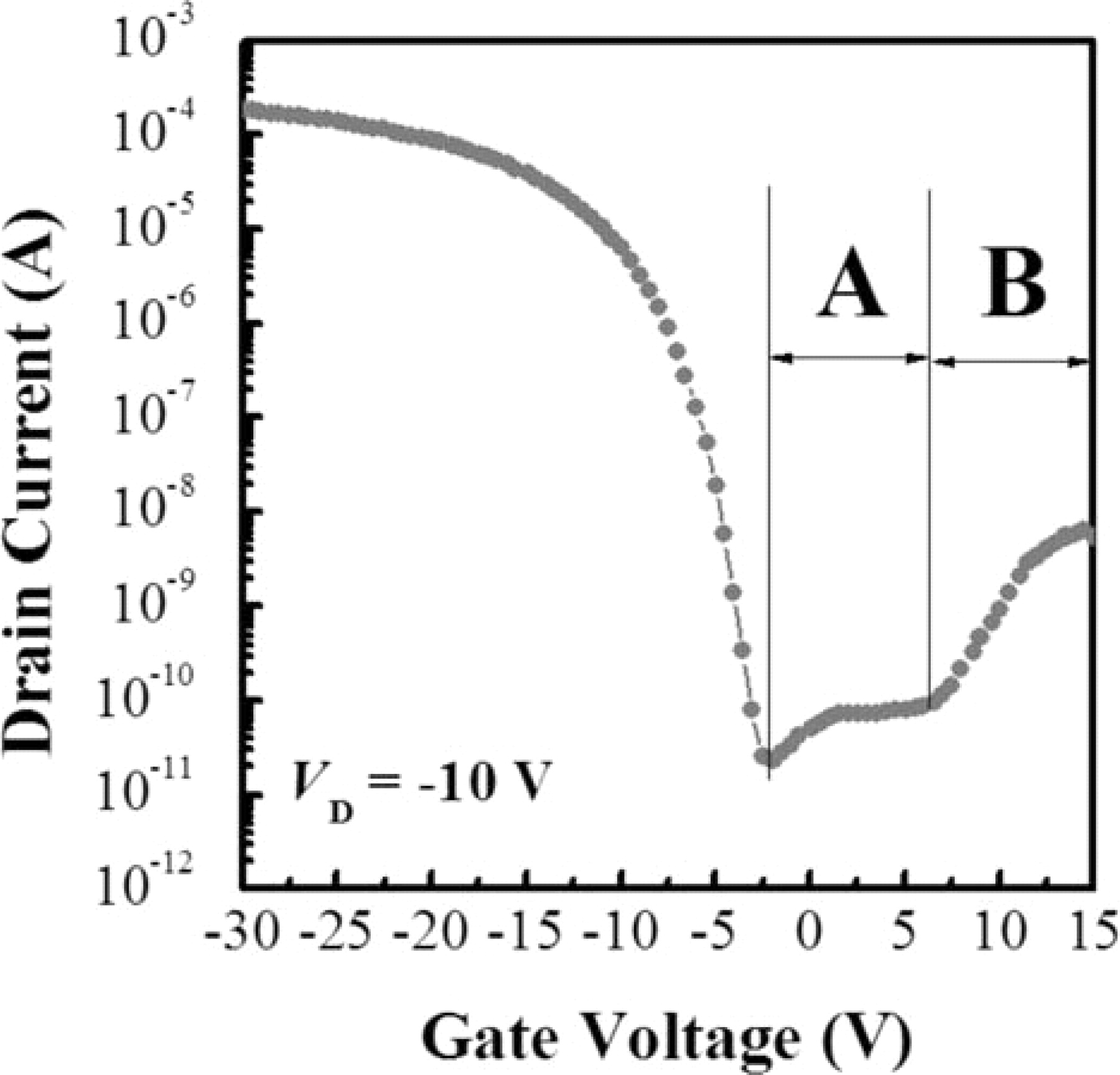
Figure 2. Typical ID-VG transfer curves of conventional MILC poly-Si TFT.
Fig. 3 shows the comparison of the ID-VG transfer curves of SIC, SA-SILC and OS-SILC poly-Si TFTs. It was surprising that SIC and SA-SILC did not show much difference in ID-VG transfer curves. However, threshold voltage was lower by about 2.5 V in OS-SILC as compared to the other two. The on-state current was almost the same for each group. The on-state current is not affected by Ni silicide defect concentration, compared with the leakage current, which is much more dependent on the concentration of Ni silicide defects.17 As for the behavior of the leakage current, SIC showed a bump and a low pinning current. On the other hand, SA-SILC showed no bump, but the pinning current was relatively high. The minimum leakage current for each was about the same at VD < −5 V; but at VD > −5 V, OS-SILC showed the lowest minimum leakage current. The minimum leakage current increased more rapidly in SA-SILC and SIC than in OS-SILC, as shown in Fig. 4. It means that the trapped carriers are minimized by OS-SILC. The OS-SILC showed a flat region A, and no pinning was observed in the Fig. 3. Similar ID-VG characteristics for SIC and SA-SILC indicate that, even for the blanket deposition of Ni, the seed cannot be formed continuously on the surface of a-Si because of which, in practice, the lateral growth occurs during crystallization, even in the case of SIC. However, because there was a bump in region A in the case of SIC, and there was no bump in SA-SILC, there was a slight difference in the amount of trapped Ni silicide between these two groups. Less trapping of Ni silicide at the grain boundaries in the channel was expected in OS-SILC than in SIC or SA-SILC; this was confirmed by the lower threshold voltage observed in this group than in the other two. Since the pinning phenomenon is related to the amount of Ni silicide traps between channel and drain junction, it was not seen in OS-SILC.
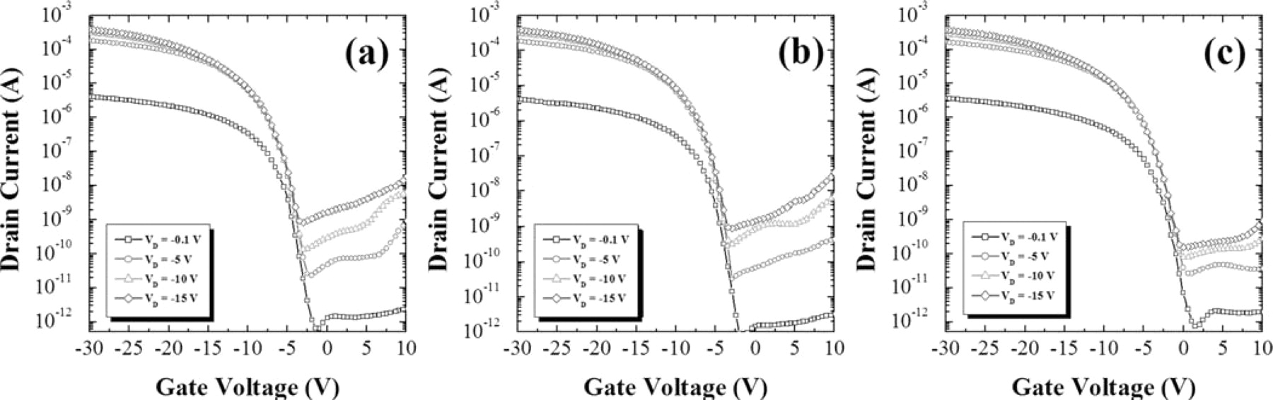
Figure 3. Comparison of ID-VG transfer curves of (a) SIC, (b) SA-SILC, and (c) OS-SILC.
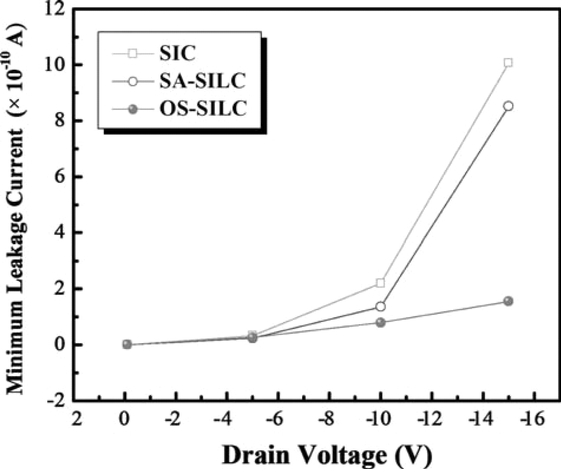
Figure 4. Dependence of the minimum leakage current of SIC, SA-SILC, and OS-SILC as increasing of drain voltage.
Fig. 5 shows the comparison of the ID-VG transfer curves of MIC, SA-MILC and OS-MILC poly-Si TFTs. The on-state current was the lowest in SA-MILC and the highest in OS-MILC, regardless of drain voltage. The leakage current level in MIC was more than two orders of magnitude higher than that of OS-MILC, indicating that there were far too many Ni silicide traps. In case of SA-MILC, the pinning phenomenon was so outstanding that the bump in region A was hidden under the rapid increase of the leakage current with gate voltage. Therefore, we determined that MIC and SA-MILC cannot be applied to AMOLED because the leakage current is too high. On the other hand, for OS-MILC, the on-state current of 10−4 A, the subthreshold slope of less than 1 V/dec, the mobility of 20–40 cm2/V-sec, and the on/off ratio of more than 106 are all quite acceptable for AMOLED; however, the leakage current near 10−10 A could still be a problem.
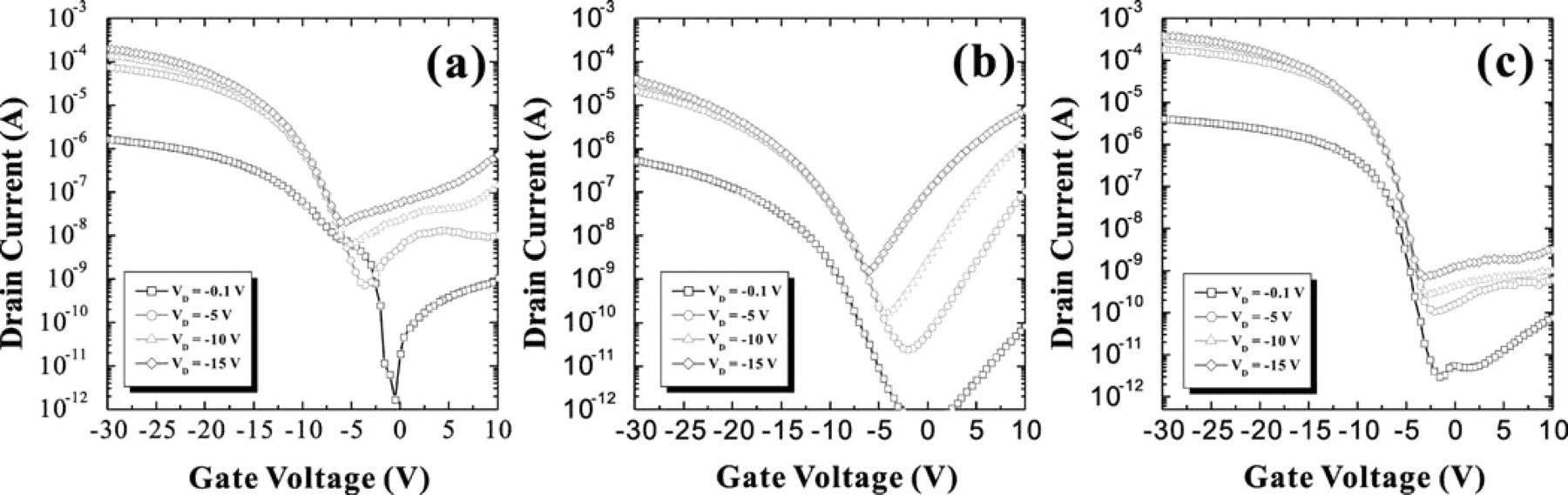
Figure 5. Comparison of ID-VG transfer curves of (a) MIC, (b) SA-MILC, and (c) OS-MILC.
The electrical parameters of MIC and SIC groups calculated from the ID-VG transfer curves are listed in Table I. 10 transistors (W/L = 10/10 μm) were selected per sample, and the electrical properties were calculated for average values. The threshold voltage was defined at a normalized drain current (ID × W/L) of 0.1 μA at VD = −10 V. The subthreshold slope, which was defined as the voltage required to increase the drain current by a factor of 10, is given by
![Equation ([1])](https://content.cld.iop.org/journals/1945-7111/159/4/J115/revision1/jes_159_4_J115eqn1.jpg)
The field-effect mobility, which was extracted from the maximum value of trans-conductance in the linear region at VD = −0.1 V, is given by
![Equation ([2])](https://content.cld.iop.org/journals/1945-7111/159/4/J115/revision1/jes_159_4_J115eqn2.jpg)
The maximum on/off current ratio was determined at VD = −10 V and VG = −30 to 10 V.
Table I. Device key parameters of the MIC, SA-MILC, OS-MILC, SIC, SA-SILC, and OS-SILC poly-Si TFTs.
| Key Parameters | MIC | SA-MILC | OS-MILC | SIC | SA-SILC | OS-SILC |
|---|---|---|---|---|---|---|
| Field-effect mobility μFE (cm2/V-s) | 29.8 | 17.5 | 66.3 | 63.3 | 63.4 | 63.2 |
| Threshold voltage VTH (V) | 10 | 9 | 7.5 | 7.5 | 7.4 | 5.5 |
| Subthreshold slope S. S. (V/dec) | 1.5 | 1.6 | 0.9 | 0.7 | 0.8 | 0.8 |
| Drain current @ VG = 0 V ID (×0−10 A) | 220 | 26 | 4.1 | 8.6 | 3.0 | 0.8 |
| Maximum on-current Ion (×0−4 A) | 1.4 | 0.3 | 2.7 | 3.0 | 3.1 | 2.8 |
| Minimum leakage current ILeak (×0−10 A) | 69 | 1.6 | 2.7 | 1.3 | 3.2 | 0.8 |
| Pinning current @ VG = 15 V IPinning (×0−8 A) | 215 | 753 | 0.70 | 6.89 | 8.80 | 0.78 |
From this, we can see relatively low mobility in the case of MIC and SA-MILC due to high concentration of trapped Ni silicides. Other than these two cases, more than 60 cm2/V-sec can be obtained for the electrical mobility. As the concentration of Ni silicides got smaller, threshold voltage became lower. It is obvious from this table that MIC contained the highest concentration of trapped Ni silicides at the channel and OS-SILC contained the lowest, as was expected. The on-state current has little influence on the concentration of Ni silicides, and the pinning current can be reduced by offsetting the Ni deposition from the gate edge. It was surprising to notice that SIC poly-Si TFT shows low pinning current without offsetting, which was different from MIC and SA-MILC poly-Si TFTs. This strongly suggests that the seed did not form continuously on a-Si thin film in SIC, and that the lateral growth was the predominant mechanism, even at the area where Ni was once deposited before the heat-treatment. Since the electrical parameters of SIC poly-Si TFT are quite acceptable, if not better than OS-SILC poly-Si TFT, it shows great promise in terms of mass production capabilities. This suggests that no extra mask step is necessary for mass production, which could make a big difference in the industry.
In Fig. 6, ID-VG transfer curves of SA-MILC and SA-SILC poly-Si TFTs are compared. SA-MILC showed higher leakage current and lower on-state current than SA-SILC in the case of self-aligned Ni deposition. The pinning phenomenon was more outstanding in SA-MILC due to relatively larger number of Ni silicide traps between channel and drain junction,19 and it roles as potential barrier to flow of carriers. the SA-SILC was expected to also contain a large number of Ni silicide traps because it was also a self-aligned process; however, the Ni was removed immediately after the deposition, thus the number of Ni silicide traps between channel and drain junction should be far fewer than SA-MILC. In the case of SA-SILC, we did observe the bump in region A, which is an indication that the Ni silicide traps in the channel were much smaller than SA-MILC. We have not yet identified the nature of the seed that was formed, but we are currently investigating what happened after Ni sputtering on a-Si at room temperature. The slope, which is directly related to the switching characteristic of the pixel, was much worse in the case of SA-MILC than in SA-SILC. In this self-align process, since the gate was used as a mask for Ni deposition, Ni silicide must have been intensively trapped at both ends of the channel. If that was the case, SA-MILC should have been much worse than SA-SILC because Ni was not removed before crystallization, and the new Ni silicide fragments could be formed continuously during heat-treatment as shown in Fig 7.
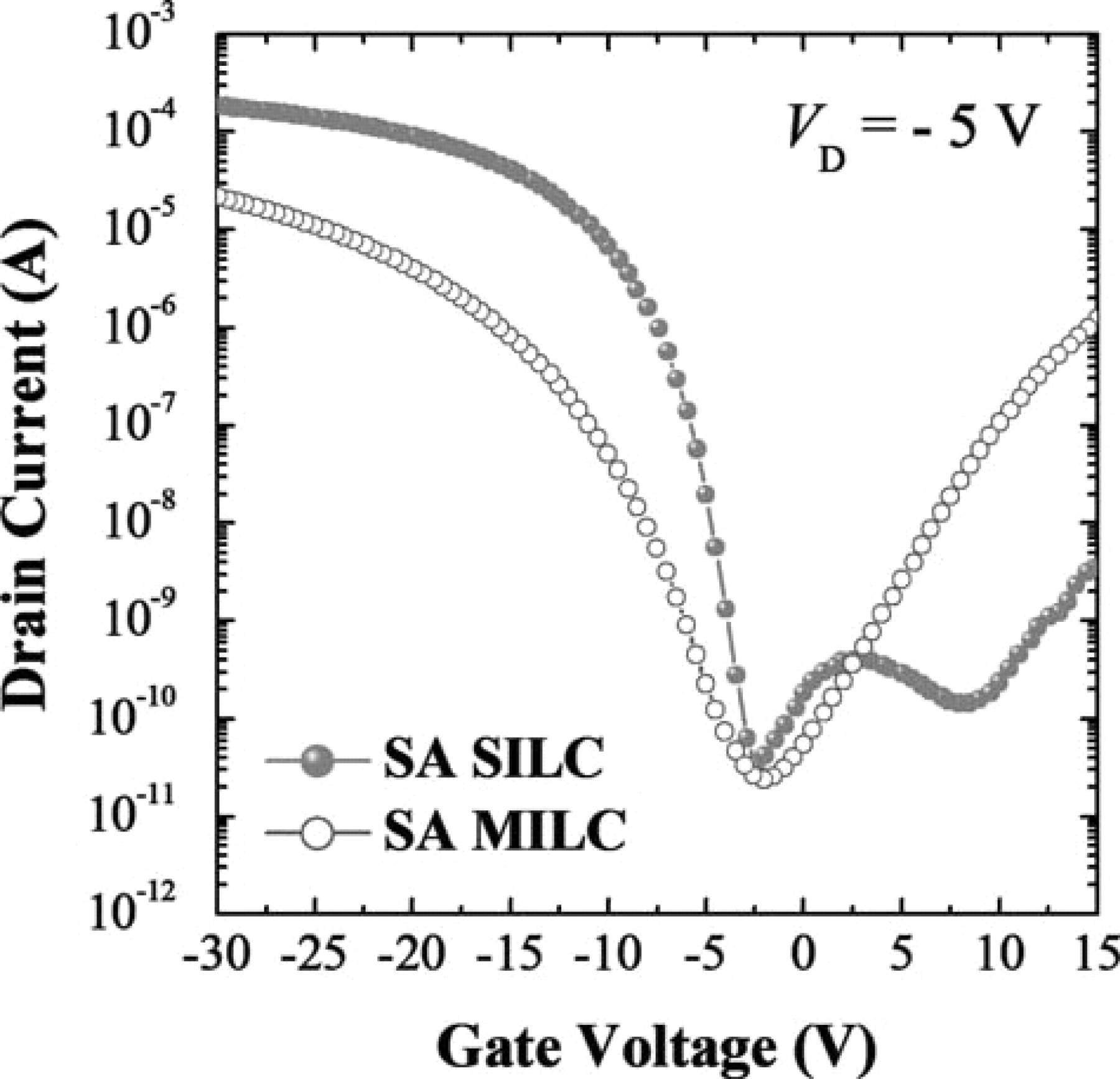
Figure 6. ID-VG transfer curves of (a) SA-SILC, and (b) SA-MILC at VD = −5 V.
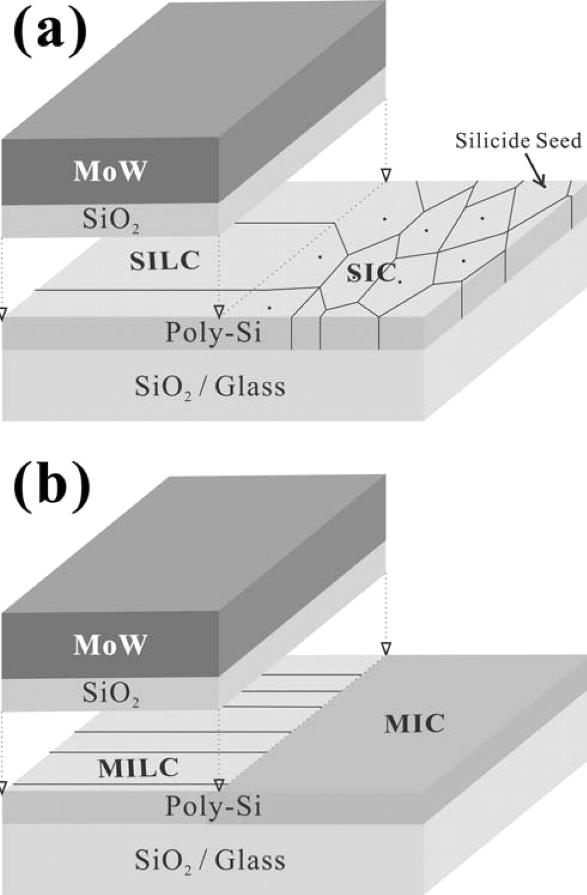
Figure 7. Schematic diagrams of crystallization mechanisms of (a) SA-SILC and (b) SA-MILC. The gate was lifted to reveal the channel area crystallized by SILC and MILC.
For the off-set process, SILC and MILC are compared in Fig. 8. OS-SILC showed lower leakage current than OS-MILC, but there was no difference in the on-state current. Reduction in threshold voltage by about 2.5 V was observed in OS-SILC as compared with OS-MILC. This could have been due to the difference in the amount of trapped Ni silicides between the two. The pinning current was almost the same, which might indicate that trapping of Ni silicide proceeds to a certain extent even though supply of Ni is stopped during the heat-treatment. In order to compare the number of defect from trapped Ni silicide in the channel, which is the cause of the leakage current, the interface trap state density (NT) was determined using a Levinson plot,20 which can estimate the NT from the slope of a linear regime of ln(ID/VG) versus 1/VG at low VD (= −0.1 V) and high VG (over threshold voltage) values. The plots were given by :
![Equation ([3])](https://content.cld.iop.org/journals/1945-7111/159/4/J115/revision1/jes_159_4_J115eqn3.jpg)
where W, L, and t are the channel width, length, and semiconductor thickness, respectively. As shown in Fig. 9, the NT of the OS-SILC poly-Si TFT was 1.9 × 1012 cm−2, which was much lower than that of the OS-MILC poly-Si TFT (2.3 × 1012 cm−2). As we mentioned before, the interface NT, which is the dominant leakage source and results from Ni silicide trapped defects in the channel, is drastically reduced by the SILC process and the comparison of SILC with MILC is consistent with their electrical performances.
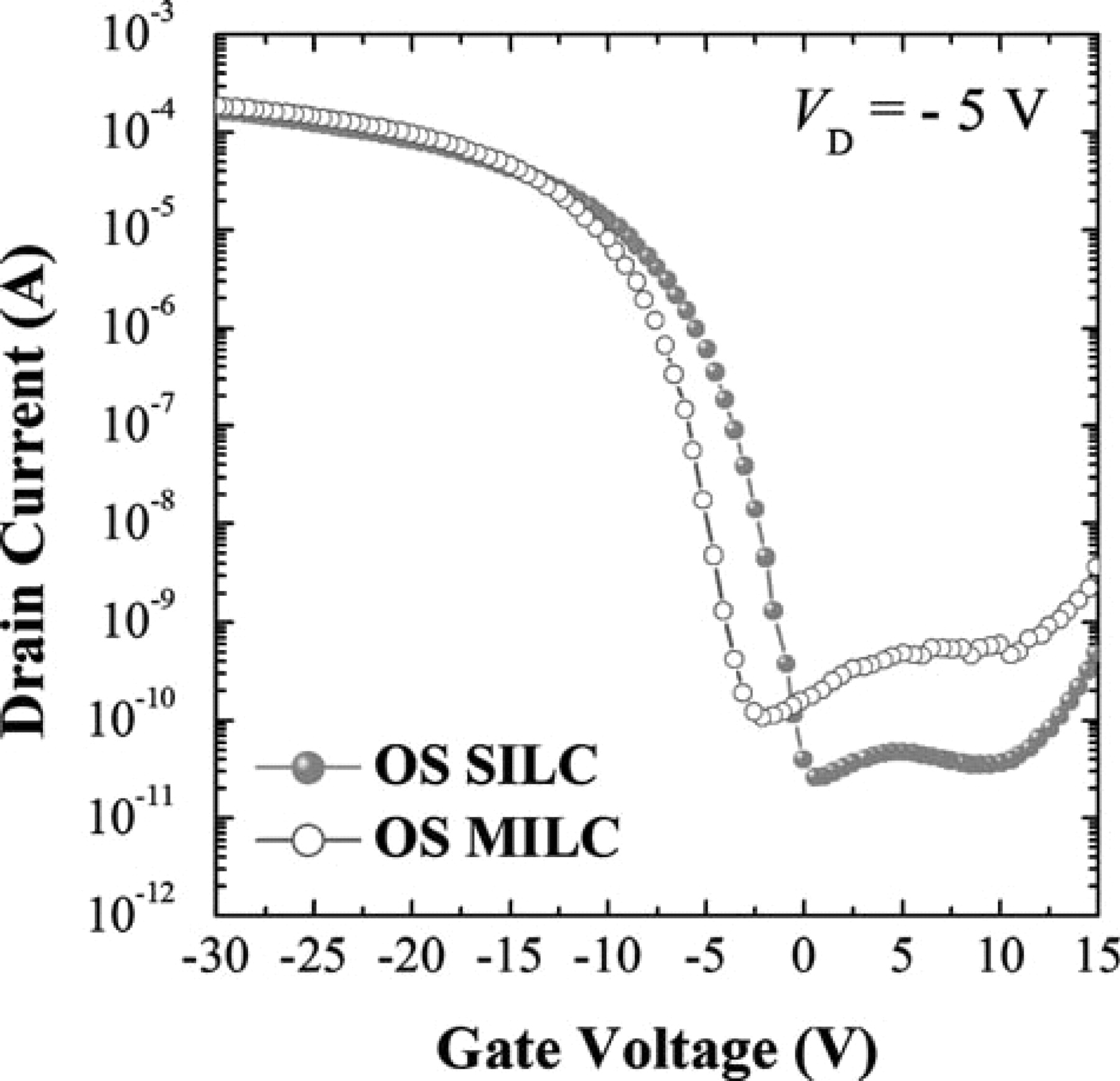
Figure 8. ID-VG transfer curves of (a) OS-SILC, and (b) OS-MILC at VD = −5 V.
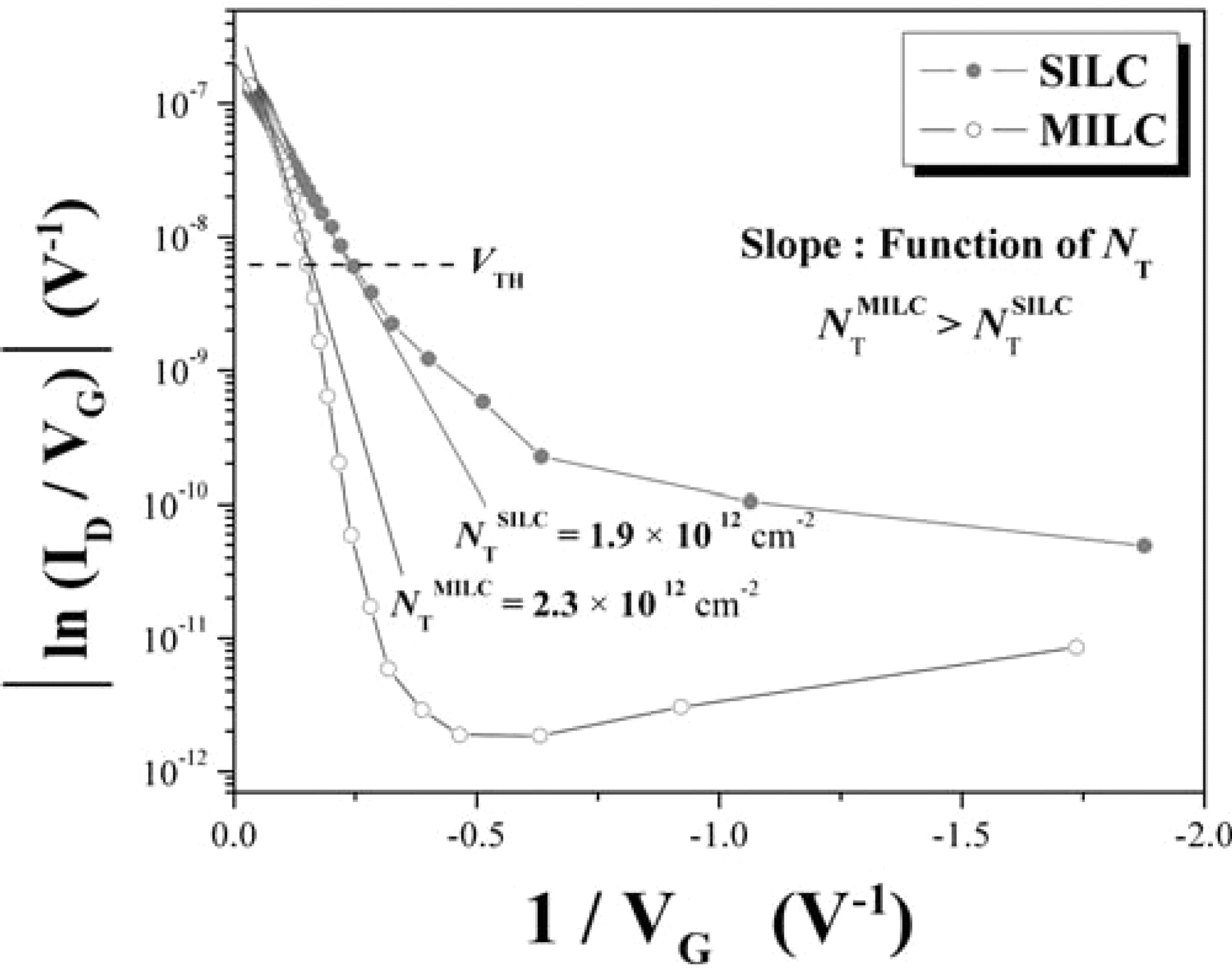
Figure 9. Levinson plot of ln(ID / VG) vs. (1 / VG) for OS-MILC and OS-SILC poly-Si TFTs. ID measured at VD = −0.1 V.
In order to find causes of better electrical properties of OS-SILC than that of OS-MILC, material was analyzed using Raman scattering spectroscopy and field emission scanning electron microscopy (FESEM). Fig. 10 shows Raman spectra of a-Si and poly-Si films crystallized by MIC, MILC, SIC and SILC. The spectrum of the a-Si showed a broad structure near 480 cm−1, with a full-width-at-half-maximum (fwhm) of about 60 cm−1. The spectrums of the MILC and SILC poly-Si thin films each had a peak centered at 519.67 cm−1 and 519.38 cm−1 with fwhm values of 8.2 cm−1 and 6.1 cm−1, respectively. Also, the MIC poly-Si thin film had a peak centered at 520.86 cm−1 with a fwhm value of cm−1, which was larger than the value of the peak centered at 520.52 cm−1 with a fwhm value of 7.6 cm−1 obtained for the SIC poly-Si thin film. The absence of the broad peak centered at 480 cm−1 for the MIC, SIC, MILC, and SILC thin films indicated that the a-Si thin film was fully crystallized by those crystallization methods after annealing. To better analyze this characteristic in the poly-Si thin films, we calculated the crystalline fraction (Xc) from the integral intensities of the Raman spectra, which is defined as follows:21
![Equation ([4])](https://content.cld.iop.org/journals/1945-7111/159/4/J115/revision1/jes_159_4_J115eqn4.jpg)
In this equation, Ia and Ic are the amorphous and crystalline integral intensities of the Raman spectra, respectively, and to take into account the different Raman scattering cross section of amorphous and crystalline phases, Ia is multiplied by a correction factor γ. In this study, the value 0.8 was utilized for γ.22
![Equation ([5])](https://content.cld.iop.org/journals/1945-7111/159/4/J115/revision1/jes_159_4_J115eqn5.jpg)
As shown in Fig. 5, the crystalline fraction of SILC (96.69%) is higher than that of MILC (95.24%); while, the SIC and MIC regions exhibit lower percentages of crystalline fraction (94.53% and 82.54, respectively) than those of SILC or MILC. Notably, the MIC region has the lowest crystalline fraction among those regions, which turned out to contain much of the Ni silicides as defects. This result was confirmed from the results of the fwhm comparisons.
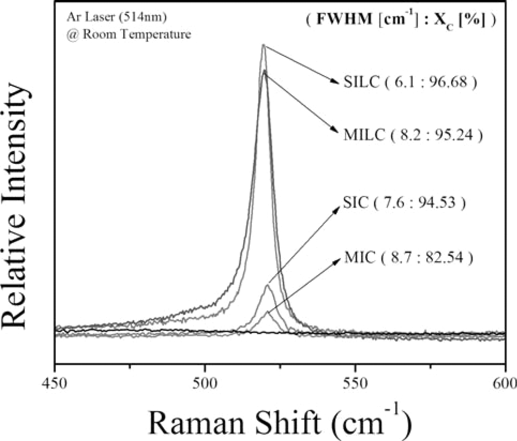
Figure 10. Raman spectra of a-Si film and poly-Si films crystallized by MIC, MILC, SIC, and SILC.
A smaller fwhm value means a better polycrystalline quality. SILC turns out to be the best among these poly crystals. This might indicate that SILC has the largest grain size with the fewest grain boundaries. This fwhm is also related to the concentration of Ni silicide trapped at the grain boundaries so that it can be concluded that SILC shows the lowest defect concentration among these polycrystallines.23
To observe the surfaces of MILC and SILC poly-Si samples using FESEM, samples were Secco etched after crystallization annealing at 550°C for 4 h. It is known that Secco etchant can etch α-Si and Ni silicide from crystalline Si selectively.24 In Fig. 11, FESEM images of MILC and SILC regions are shown. It is obvious that the MILC region contains more Ni silicides than the SILC region and the Ni silicides trapped at the grain boundaries make large holes after the Secco etch. Lateral growth occurs by the catalytic reaction of the Ni silicide, not by diffusion of Ni into the a-Si, so we cannot find Ni silicide inside the poly-Si grain. But lateral growth would stop when the catalyst comes across other poly-Si grain boundaries and the Ni silicide would be trapped at the grain boundaries, because there is no chemical potential-driving force for the phase transformation between the two poly-Si grains.25 The presence of trapped Ni silicide in the channel region of the TFTs degrades the leakage current in MILC poly-Si TFTs.26,27 It may be also noticed that SILC exhibits longer grains than MILC because SILC starts with a lower concentration of Ni silicide at the lateral growth front than does MILC. It is well known that, as more short grains are utilized to make grain boundaries, the grain boundaries trap charge carriers and buildup potential barriers to the flow of carriers.28 In light of this previous result, longer grains of SILC compared to those of MILC would yield better electrical performances.
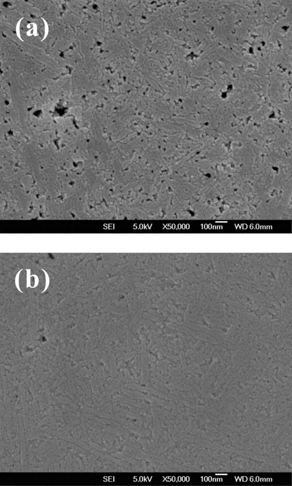
Figure 11. FESEM images of (a) MILC and (b) SILC regions. The Ni silicide was etched away by Secco etchant.
More research work is underway to find the nature of the seed formed after sputter of a Ni on a-Si thin film at room temperature, and how these seeds can survive after the direct etch of Ni prior to crystallization and act as a catalyst for phase transformation.
Conclusions
Ni silicides trapped at the grain boundaries play a critical role in deteriorating the electrical performance of a poly-Si TFT fabricated by metal-induced lateral crystallization. In this work, we devised a new way of reducing the amount of Ni silicide trapped at the grain boundaries of the poly-Si, named seed-induced lateral crystallization (SILC). The best electrical performance can be obtained using OS-SILC. OS-SILC poly-Si TFT has improved electrical parameters, including the field effect mobility of 63 Cm2/V-sec, the leakage current of 7.9 × 10⁻¹¹ A, the slope of 0.8 V/dec, Ion of 2.8 × 10⁻⁴ A at VD = 10 V, and VTH of 5.5 V, all of which are comparable to those of the laser poly-Si TFTs. By systematic studies carried out in this work, we have distinguished two regions in the leakage current, and the relationship between the concentration and location of the defects within these two regions was revealed. The silicide seed-induced laterally crystallized poly-Si has good crystallinity and a higher crystalline fraction. In addition, it can be noticed that the interface trap density of the poly-Si thin film crystallized by SILC is lower than that of the poly-Si thin film crystallized by MILC due to the lower Ni silicide concentration. Most promising, the SIC poly-Si TFT (where no extra mask step was required) showed reasonable electrical performance suitable for AMOLED. Hence, it is expected that the mass production of poly-Si TFTs for AMOLED will be quickly realized through the SIC process in the near future.
Acknowledgment
This work was supported by the National Research Foundation of Korea (grant no. RIAMI-AM37-11), Ministry of Knowledge Economy of Korea (grant no. RIAMI-AC16-11) and the Brain Korea 21 (BK21) program. The authors acknowledge the experimental help from the Samsung Corning Precision Materials Co., Ltd. and Eui-San Research Center at Seoul National University, Seoul, South Korea.