
Abstract
The ability to systematically vary the flatband potential and the band edge positions of Cu2O by varying the deposition bath pH is considered important in the context of using Cu2O for photocatalytic water splitting. Capacitance-voltage (C-V) and dark and light current-voltage measurements were taken in order to investigate the electronic properties of electrodeposited Cu2O thin films grown in an acetate bath containing a 0.01 M Cupric Acetate having different bath pH values. The Mott-Schottky plots resulting from C-V measurements revealed that the flatband potential and doping density of the films strongly depended on the deposition bath pH. For pH values lower than 7.2, conductivity of Cu2O films remained n-type while it changed to p-type for higher pH values indicating that change of n-type to p-type character of the Cu2O films can be controlled by the bath pH. With increasing pH value, the grain size decreased, while crystal shapes transformed from truncated octahedral to cubic within the tested pH range. A well ordered cubic structure was observed in films deposited at pH 7.8. The rate of deposition decreased at higher pH values leading to thinner films indicating the effect of pH on the film thickness. Calculated band edge positions of conduction and valance bands of the Cu2O films were −4.19 eV and −6.29 eV respectively with respect to the vacuum level.
Export citation and abstract BibTeX RIS
Hydrogen is considered one of the most promising alternative energy sources that have the potential to withstand the future energy challenges.1–4 Availability of sun light as a continuous source of energy enables producing hydrogen through photo catalytic water splitting.5 Among the various photocatalytic systems, metal oxide based semiconductor catalysts have received a wider attention due to their easy fabrication and associated low cost. However, it has been a challenge to find a suitable metal oxide semiconductor for visible light driven hydrogen evolution reaction (HER) and oxygen evolution reaction (OER).6,7 To achieve the overall water splitting reactions, the conduction band energy and the valance band energy of a single semiconductor material should be compatible with the electrochemical potentials of E° (H+/H2) and E° (O2/H2O) to drive the HER and OER reactions.8 That is, the bottom of the conduction band of the semiconductor should be located at a more negative potential than the redox potential of E° (H+/H2) and the valence band edge of the semiconductor must remain above the redox potential of E° (O2/H2O).6,9 A theoretical semiconductor bandgap energy of 1.23 eV is required to drive the overall water-splitting reaction.6,8,10 However, due to loss mechanisms in electron-transfer processes such as series resistance and the electro catalytic overpotentials at semiconductor/liquid junctions the energy required for photocatalytic water splitting at a semiconductor photo electrode is reported to be in the range of 1.6–2.4 eV.8,10
Cuprous Oxide (Cu2O) is a direct bandgap semiconductor with a narrow bandgap (Eg = 1.9–2.2 eV) in which the conduction and valence band positions are compatible for photocatalytic water splitting. The relatively high absorption coefficient of Cu2O makes it a promising material for photocatalytic water splitting.10–14 Therefore, Cu2O is in principle capable of decomposing water into H2 and O2 under visible light excitation. Its natural abundance, non-toxicity and ability of large area fabrication at low temperature and at low cost using methods such as electrodeposition11,12,15–18 makes it even more appealing as a material for the above purpose. Cu2O is natively a p-type semiconductor due to either copper-vacant or oxygen-rich conditions.16,19,20 However, the electrodeposition technique has enabled the fabrication of both n-type and p-type Cu2O films.21,22 Jayathileke et al. have demonstrated that the pH can restrain copper vacancies and populate oxygen vacancies in Cu2O, thereby controlling the amount of oxygen incorporated to yield n-type Cu2O.16,23–25
Several methods for studying semiconductor/electrolyte interfaces are available, the predominant ones being dark current and photocurrent measurements as a function of the potential difference, and capacitance-voltage measurements(C-V).24–26 Although there are many reports available on the observation of p-type and n-type conductivity of Cu2O thin films,15,16,20,26 there are no reports available yet, to our knowledge, on the systematic characterization of tunable parameters such as the effective donor (ND) or acceptor density (NA) and flatband potential (VfB) of Cu2O films with respect to the deposition bath pH. This paper emphasizes such a characterization that will enable to optimize Cu2O related parameters directed at using the material as an efficient solar water splitter.
Experimental
Potentiostatic electrodeposition (Hokuto-Denko-Potentiostat/Galvanostat-HA 301) of Cu2O thin films on Ti substrates (area ∼1 × 1 cm2) that worked as the working electrode was carried out in a three electrode electrochemical cell containing 0.1 M sodium acetate (Sigma-Aldrich, purity ≥ 99.0%) and 0.01 M cupric acetate(Sigma-Aldrich, purity ≥ 99.0%) aqueous solution at −200 mV with respect to a Ag/AgCl reference electrode for 40 min by maintaining the temperature of the bath at 55°C. The counter electrode was platinum plate and the electrolyte was continuously stirred using a magnetic stirrer.16 Electrolytic solutions were prepared using deionized water. Ti substrates used for film deposition were cleaned with detergent, diluted HCl, distilled water and by ultrasound sonication. pH of the deposition bath was measured using a SPER Scientific pH meter and varied (5.8 to 8.0) by adding a dilute solution of sodium hydroxide or acetic acid. Upon deposition of films, electrodes were immediately washed using deionized water and dried in air. Photorepsonse measurements of the samples were made in a three electrode photoelectrochemical cell (PEC) containing a 0.1 M sodium acetate aqueous solution. The counter electrode was a platinum plate with an Ag/AgCl reference electrode. The dark and light current–voltage characteristics of the samples were simultaneously measured by chopping white light (1.5 AM). The surface morphological features of the samples were monitored by scanning electron microscopy (SEM) (Zeiss Evols15) and their structure was determined by high energy X-ray diffraction (HEXRD). The HEXRD experiments were performed using beamline BL04B2 at SPring-8, Japan with incident X-rays of wavelength of 0.20202 Å (energy ≃61.374 keV) using a Si (220) monochromator. The intensity of the incident X-ray beam was measured using an ionization chamber filled with Ar gas of 99.99% purity. The samples HEXRD measurements were prepared by pealing off electrodeposited Cu2O thin films from Ti substrates and filling in to silica capillary tubes of 1 mm internal diameter × 0.01 mm thickness × 80 mm length. During measurements, samples were held in a vacuum bell jar to avoid scattering of X-rays in air, and the intensity of diffracted X-rays was measured using four CdTe and two Ge detectors that cover measurements in a wider angular range with extremely low background.27
The C-V measurements of thin film electrodes were carried out at a frequency 1 kHZ using a surface area of 1 mm2 of each sample. Gamry Series G 300 Potentiostat controlled by EIS300 software (Gamry Instruments, Inc.) was employed to take C–V, dark and light current–voltage and Electrochemical impedance spectroscopy (EIS) measurements. EIS measurements were taken using the same configuration as for the PEC measurements in 0.1 M KCl solution containing 0.5 mM K3[Fe(CN)6]/K4[Fe(CN)6]. The equivalent circuit modeling and curve fitting was achieved with Echem Analyst software (Gamry Instruments, Inc.). The measurements were made at an applied potential of −0.003 V vs. Ag/AgCl under ambient light illumination by providing AC perturbations of amplitude 10 mV in the frequency range of 0.01–100 kHz.
Results and Discussion
In order to develop an efficient solar water splitting system, the energy band positions in the semiconductor and the electrolyte should be compatible. When an n-type semiconductor comes in contact with a redox couple, Fermi energy levels align with each other due to transfer of electrons from the semiconductor to the electrolyte resulting in band bending in the semiconductor at the interface. Consequently, the semiconductor becomes more positively charged giving rise to a space charge region with the formation of a negatively charged sheet at the electrolyte interface. Application of a forward biased voltage (eg. using a potentiostat) causes the Fermi levels of the semiconductor and the electrolyte to separate decreasing the level of band bending. When the bias voltage is such that there is no band bending, or charge depletion, the semiconductor reaches its flatband potential, VfB. The state of flatband potential of a semiconducting thin film in contact with an electrolyte is characterized by a zero photocurrent due to the inability to separate photogenerated carriers in the semiconductor in the absence of a depletion region which provides the necessary electric field. The flatband potential, VfB associated with a p-type semiconductor in contact with an electrolyte can be explained in a similar manner.28
Experimentally, the flatband potential can be determined by making C-V measurements that lead to Mott–Schottky plots. The Mott–Schottky equation is derived from the Poisson's equation by using the Boltzmann equation and Gauss' law which accounts for the distribution of electrons in the space charge region and the electric field through the interface to the charge contained within that region.29
![Equation ([1])](https://content.cld.iop.org/journals/1945-7111/166/4/D113/revision1/d0001.gif)
In the Mott–Schottky equation, C is the interfacial capacitance, A is the film area, ND is the doping density, V is the applied voltage, kB is the Boltzmann constant, T is the absolute temperature, e is the electronic charge, εo is the vacuum permittivity and εis the dielectric constant of Cu2O. Therefore, a plot of 1/C2 against V should yield a straight line from which VfB can be determined from the intercept on the V axis. The value of ND can also be conveniently found from the slope knowing ɛ and A.
Figure 1 shows the Mott–Schottky plots for Cu2O films electrodeposited in an acetate bath in a range of pH values varying from pH 5.8 to 8.0 and the inset shows the dark and light current–voltage characteristics obtained for the same sample. At each pH value, the flatband potential found from the onset potential of photocurrent in dark and light current-voltage characteristic curve and the intercept of extrapolated line in the linear region with the potential axis in the Mott-Schottky plot are shown in Table I. Simultaneously, the conductivity type of the films at each pH value was determined by using the sign of the gradient of the linear region of the Mott-Schottky plots. The Mott-Schottky plots showed that the extrapolated flatband potential of Cu2O films was strongly dependent on the pH of the deposition bath. Combination of the dark and light current-voltage measurements and Mott-Schottky plots revealed that the Cu2O films remained n-type until the pH of the deposition bath was around 7.0. Then the conductivity changed into p-type when the bath pH was increased above 7.2. This change in conductivity around a deposition bath pH 7.0 agrees reasonably well with the previously obtained results made using the spectral response measurements.15,16 It is worth noting that from the previous work of Jayathilake et al.,15 under higher electrolyte pH levels, a significant increase in the acceptor density makes the deposited Cu2O films p-type due to the formation of Cu vacancies. However, their work further shows that even under lower bath pH, maintaining a low enough concentration of Cu ions will lead to the formation of p-type Cu2O films. This highlights the role of Cu ion concentration when forming p-type Cu2O films. It is clearly seen from Table I that the onset potential of the photocurrent value has always shifted to more negative values with respect to the extrapolated flatband potential when the deposited film is n-type and to more positive values when the deposited film is p-type. This is attributed to the creation of surface states at the Cu2O/electrolyte interface and hence pinning the Fermi level.26,30 The extrapolated flatband potential has been obtained with respect to an Ag/AgCl reference electrode and hence the exact position of the Fermi level with respect to the normal hydrogen electrode (NHE) or vacuum can be calculated.31
![Equation ([2])](https://content.cld.iop.org/journals/1945-7111/166/4/D113/revision1/d0002.gif)
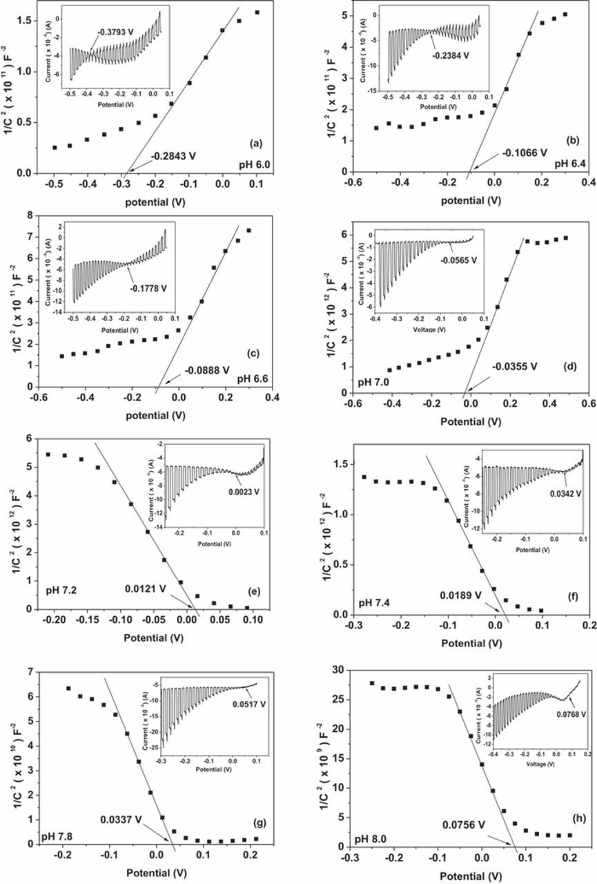
Figure 1. Mott–Schottky plot of n-Cu2O films prepared by electrodeposition in an acetate bath of pH (a) 6.0 (b) 6.4 (c) 6.6 (d) 7.0 (e) 7.2 (f) 7.4 (g) 7.8. (h) 8.0. The inset shows the dark and light current–voltage characteristics of the same Cu2O sample.
Table I. Extrapolated flatband potential and onset potential of the photocurrent variation with the deposition bath pH.
| pH of the deposition bath | Extrapolated flatband potential (mV) | Onset potential of the photocurrent (mV) |
|---|---|---|
| 5.8 | −440 ± 32 | −450 ± 0.001 |
| 6.0 | −284 ± 17 | −379 ± 0.001 |
| 6.2 | −197 ± 23 | −335 ± 0.001 |
| 6.4 | −106 ± 19 | −238 ± 0.001 |
| 6.6 | −89 ± 17 | −177 ± 0.001 |
| 6.8 | −43 ± 26 | −91 ± 0.001 |
| 7.0 | −35 ± 12 | −56 ± 0.001 |
| 7.2 | 12 ± 5 | 23 ± 0.001 |
| 7.4 | 19 ± 7 | 4 ± 0.001 |
| 7.6 | 25 ± 7 | 46 ± 0.001 |
| 7.8 | 33 ± 9 | 51 ± 0.001 |
| 8.0 | 75 ± 10 | 77 ± 0.001 |
At each pH value, the donor, ND, (acceptor, NA) density was determined from the slope (S) of the Mott–Schottky plots and using Equation 2, that was deduced from the Mott-Schottky Equation 1. The dielectric constant of n-type Cu2O and p-type Cu2O was assumed to be independent of conductivity. The dielectric constant of Cu2O was taken as ɛ = 7.6.32
The experimentally determined donor and acceptor concentrations allow calculation of the energy difference between the bottom of the conduction band, EC, and EF for n-type films and the energy difference between EF and the top of the valence band, EV, for p-type films.28
Figures 2a and 2b shows the variation obtained for (EC - EF) and (EF - EV) with the donor and acceptor concentration respectively with respect to the vacuum. These variations illustrate that the Fermi energy level of Cu2O thin films having n-type and p-type conductivity can be tuned within the conduction band and valance band. After calculating the exact position of Fermi level, the energy level positions of conduction band and valance band were calculated assuming that the energy gap of Cu2O is 2.1 eV.33 The calculated values of EC and EV were found to be −4.19 ± 0.01eV and −6.29 ± 0.01 eV respectively with respect to the vacuum level. These values were in good agreement with previously reported values in literature.34
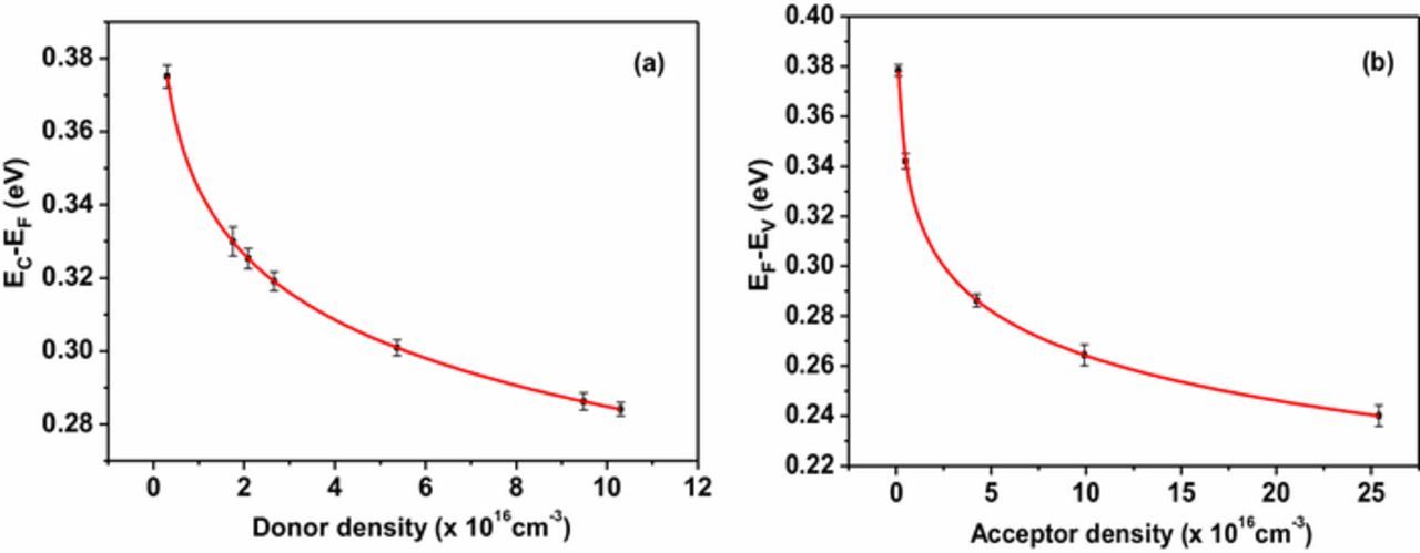
Figure 2. Variation of (a) EC- EF vs. donor density of n-type conductivity and (b) EF-EV vs. acceptor density of p-type conductivity.
It was also observed that the pH value of the deposition bath had an effect on the morphology of the electrodeposited Cu2O thin films. Figure 3 shows the SEM images of Cu2O thin films electrodeposited in the acetate bath at different pH values from 5.8 to 8.0. When the pH value of the deposition bath was greater than 8.0, precipitation occurred depriving the growth of Cu2O thin films. When the pH value was lower than 5.8, deposition of Copper initiated indicating that the pH range from 5.8 to 8.0 was suitable for deposition of Cu2O polycrystalline thin films having different grain shapes. It was noticeable from Figure 3 that the size of the Cu2O grains was typically of the order of a few micrometers with the truncated octahedral shapes at the deposition bath pH of 5.8. However, subsequent SEM micrographs in Figure 3 show that the grain size decreases with the increasing pH and the shape remains to be a mixture of truncated octahedral and cubo-octahedral until the pH is 6.4. At pH 6.6, SEM micrographs showed that there is no particular shape associated with the grains. However, grains began to develop cubic shapes beyond the bath pH 6.8. Formation of cubic grains of sides in the range of 200–300 nm is clearly evident at higher pH values showing distinct cubic geometries at pH values of 7.8 and 8.0 when the film thickness is smaller.
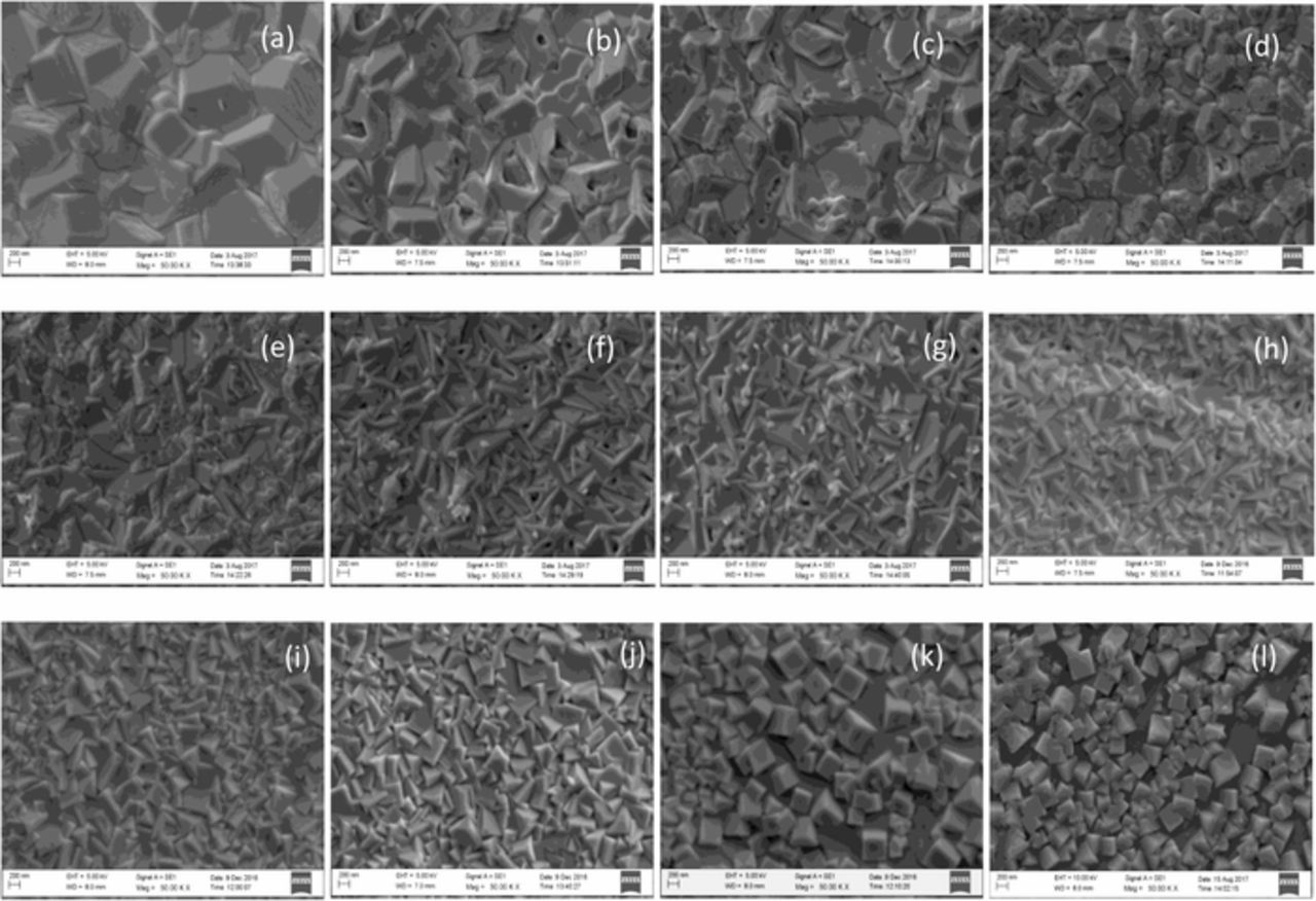
Figure 3. SEM images of Cu2O deposited at different pH values (a) 5.8 (b) 6.0 (c) 6.2 (d) 6.4 (e) 6.6 (f) 6.8 (g) 7. 0 (h) 7.2 (i) 7.4 (j) 7.6 (k) 7.8 (l) 8.0.
Figure 4 shows the HEXRD patterns of Cu2O films deposited at different pH values from 5.8 to 8.0 in the acetate bath. It shows diffraction peaks due to reflections from (110), (111), (200) and (220) planes of Cu2O at 2θ values of 3.83, 4.69, 5.42 and 7.68° respectively indicating that the films maintain the structural identity of Cu2O in this pH range. In this pH range, Cu or CuO diffraction peaks were not present in previously made conventional laboratory XRD measurements indicating that the samples were essentially Cu2O. However, a very low intense diffraction peak at 6.64° observed in Figure 4 in HEXRD spectra is due to reflections from CuO and it suggests that samples contain a CuO phase which is of very small significance. In order to calculate the lattice parameters and unit cell volumes of Cu2O thin films deposited at different bath pH, the HEXRD data were further analyzed using FullProf suit under the Rietveld refinement method for a Pseudo-Voigt function. The output lattice parameters and the unit cell volumes of Cu2O thin films deposited at different bath pH were 4.2613, 4.2608, 4.2607, 4.2600, 4.2562 and 4.2431 Å and 77.3818, 77.3519, 77.3471, 77.3113, 77.1026 and 76.3959 Å3 respectively for the bath pH at 6.0, 6.4, 6.8, 7.2, 7.6 and 8.0.
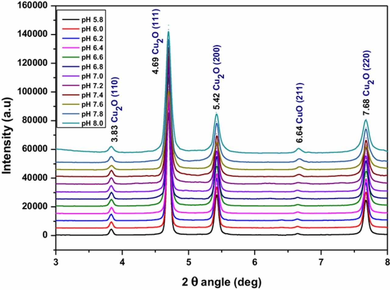
Figure 4. HEXRD patterns of electrodeposited Cu2O thin films in electrolyte containing 0.1 sodium acetate and 0.01 M cupric acetate at different pH bath values (5.8 to 8.0).
Figure 5 shows the radial distribution functions (RDFs) of electrodeposited Cu2O thin films in electrolyte containing 0.1 sodium acetate and 0.01 M cupric acetate at different pH bath. For samples, Cu-O and Cu-Cu correlations are derivable from HEXRD by mathematically converting the polarization, absorption, and background corrected HEXRD data into a total structure factor S(Q) and RDF by Fourier transformation of S(Q). For the standard Cu2O powder, the first and second peaks, identified as Cu-O and Cu-Cu correlations, have been reported at the radial distances of 1.84 and 3.02 Å respectively.35 The RDF for the Cu2O powder samples prepared by peeling off the thin film samples produced similar peak profiles and peak distances as those for the standard Cu2O powder. In this study, the first peak identified as the Cu-O correlation was found to be at 1.87 Å and the second peak identified as the Cu-Cu correlation, was found to be at 3.04 Å. The corresponding lattice parameters of Cu2O closely match with the lattice parameters reported in literature.36 Figure 5 also shows a slight gradual shift in RDF peak positions toward lower values when the bath pH is varied from 5.8 to 8.0. The observed first nearest neighbor bond distances of Cu-Cu and Cu-O were shown in the Table II. It can be seen that the peak of the first nearest neighbor Cu-Cu bond distance at 3.04 Å has remained constant until the pH 7.2 reflecting the bulk properties of the Cu2O and decreased to 2.96 Å with the further increase of pH. However, the Cu-O correlations do not show such a trend clearly and this can be expected as the Cu-O correlation peaks are of very low intensity. Results obtained through lattice parameter analysis along with Cu-Cu bond distances obtained by RDF profiles are consistent with previous observations where decreasing particle/grain size lead to decreasing bond distances due to increased surface to volume ratio that causes to reduce the repulsive interactions between atoms. This behavior is particularly significant in metallic nano-clusters.37,38
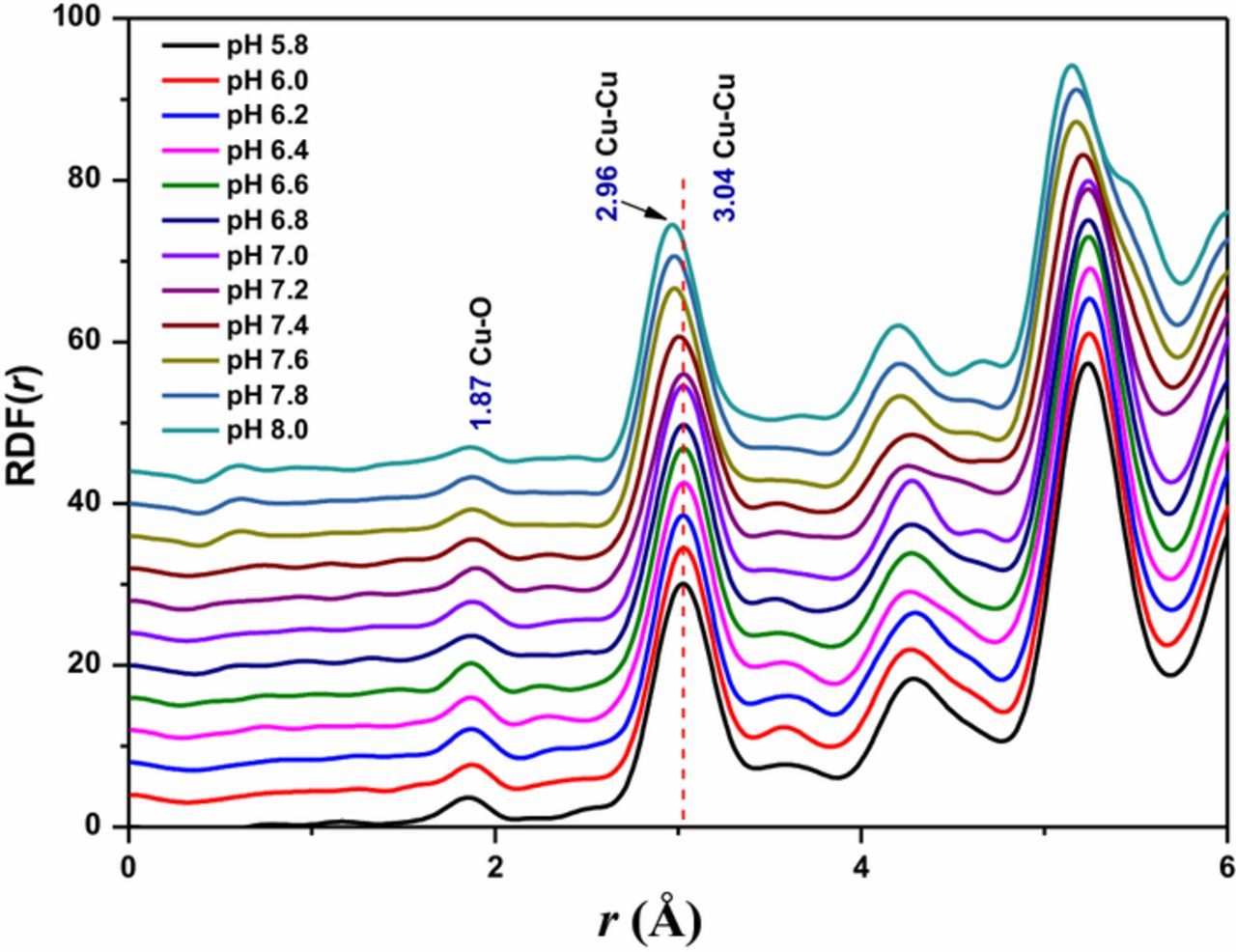
Figure 5. RDF profiles of electrodeposited Cu2O thin films in electrolyte containing 0.1 sodium acetate and 0.01 M cupric acetate at different pH bath values (5.8 to 8.0).
Table II. First nearest neighbor bond distances of Cu-Cu and Cu-O illustrate from the RDF.
| pH Bond Distance ± 0.01 | 5.8 | 6.0 | 6.2 | 6.4 | 6.6 | 6.8 | 7.0 | 7.2 | 7.4 | 7.6 | 7.8 | 8.0 |
|---|---|---|---|---|---|---|---|---|---|---|---|---|
| Cu-O | 1.86 | 1.87 | 1.87 | 1.87 | 1.87 | 1.87 | 1.88 | 1.89 | 1.88 | 1.88 | 1.88 | 1.87 |
| Cu-Cu | 3.03 | 3.03 | 3.03 | 3.03 | 3.03 | 3.03 | 3.03 | 3.03 | 3.01 | 2.98 | 2.97 | 2.96 |
Figure 6 shows Nyquist plots that were obtained using Electrical Impedance Spectroscopy (EIS) for thin films obtained at different pH values. It shows that the deposition bath pH of the thin film has a considerable effect on the properties of the catalytic surface. The impedance data were modeled by using an equivalent circuit in which a resistance Rs is connected in series with Rct|Qdl parallel circuit. Here Rs is the resistance of the electrolyte and Rct is the charge transfer resistance. The capacitive element, Qdl is a constant phase element which was used to model depressed semi circles that may have been due to heterogeneities and rough solid/electrolyte interface. It can be seen that the diameter of impedance plots become smaller with the increasing deposition bath pH implying the decreasing of the interfacial charge transfer resistance and thereby improving the catalytic activity of the electrode. The variation of charge transfer resistance can be attributed to the variation of film morphology and grain size. Increased effective surface area that has been resulted in due to smaller grains seems to have resulted in decreasing charge transfer resistance.
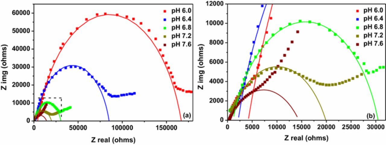
Figure 6. (a) Electrochemical impedance spectra (EIS) of electrodeposited Cu2O thin films at different pH bath where solid lines indicate the model fitted to measured data and (b) An enlarged image of the EIS spectra for higher pH values.
Figure 7 shows the variation of thickness of the Cu2O films deposited at different pH values calculated using charge vs. time plots and the Faraday's law of electrolysis.39 Uncertainty of film thickness is of the order of 10−3 μm. The rate of deposition decreases at higher pH values leading to thinner films of the order of several hundreds of nanometers as shown in Figure 7 when the deposition time is maintained constant. Therefore, it can be stated that the bath pH has an effect on the shape and size of the crystalline grains and hence on the film thickness which in turn gives rise to the observed electronic properties discussed above.
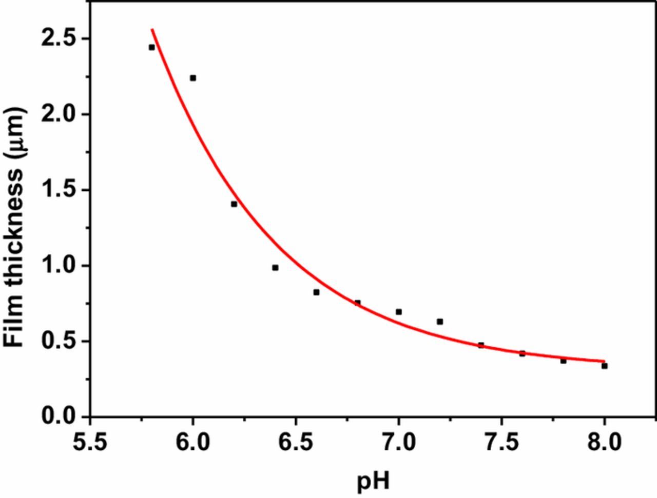
Figure 7. Film thickness variation with the deposition bath pH.
An important aspect of this study is the ability to control the shape of the Cu2O crystalline grains by changing the pH value of the deposition bath without having to use organic or inorganic surface additives. The shapes of the crystalline grains obtained in this study are consistent with those obtained by Seigfried et al. who use sodium dodecyl sulfate as an additive to the electrochemical bath containing 0.02M Cu(NO3)2.6H2O.40 As explained by Seigfried et al. different surface energies associated with the crystalline faces of the grains during their growth control the shape and hence the surface morphology of the Cu2O thin films deposited at different pH values. This ability to control the shape of the crystalline grains would provide possibilities of improving the resulting devices in such applications as photo catalysis.
Conclusions
The shape and size of the Cu2O crystalline grains of Cu2O thin films electrodeposited in an acetate bath where a 0.01 M Cupric Acetate solution was used were heavily dependent on the pH of the deposition bath. Mott–Schottky plots and dark and light current–voltage characteristics showed that the flatband potential can be systematically changed with the deposition bath pH and hence the conductivity type of the Cu2O films changed from n-type to p-type. The transition in the conductivity occured around the bath pH of 7.2 accordingly, changing the Fermi energy level positions of the films. The measurements confirmed that the Fermi level can be systematically tuned within the conduction band and valance band by controlling the deposition bath pH. The ability to control the shape of the Cu2O crystalline grains by changing the pH value leads to different surface morphologies which can be thought to facilitate the optimization of Cu2O as an efficient water splitting material.
Acknowledgment
Authors gratefully acknowledge the financial assistance provided by National Research Council of Sri Lanka through the research grant NRC16-094. R P Wijesundara of the Department of Physics, University of Kelaniya, Sri Lanka is acknowledged for the assistance provided in making some of the experimental measurements. The high-energy XRD measurements were carried out at SPring-8 with the approval of the Japan Synchrotron Radiation Research Institute (JASRI) under proposal no 2017B1539.
ORCID
J. K. D. S. Jayanetti 0000-0003-4961-0902