Abstract
Influences of pulse plating parameters on chemical composition, grain size, morphology, and mechanical property of Au–Cu alloy films electrodeposited with an Au-rich sulfite-based electrolyte were investigated. A wide range of Cu concentration (wCu) varied from 3.5 to 26.7 wt% was attained in the Au–Cu films. The galvanic displacement reaction occurred during the off-time period showed great influences on the composition and the grain size. Meanwhile, surface morphology of the Au–Cu films was interrelated with the alloy composition. An increase in the pulsed current density lead to roughening of the surface, and smoothening of the surface was achieved by promoting the displacement reaction. Micro-mechanical properties of the Au–Cu films were evaluated by micro-compression tests for applications as movable micro-components in electronic devices. A pronounced high yield strength at 1.38 GPa was achieved in the Au–Cu film with the smallest grain size at ca. 4.40 nm and the wCu at ca. 15 wt%, which is suggested to be a result of synergetic effects of grain boundary strengthening and solid solution strengthening mechanisms.
Export citation and abstract BibTeX RIS
In recent years, high density metallic materials have attracted much attention for applications as movable micro-components in micro-electro-mechanical systems (MEMS) devices to allow further enhancement in the sensitivity and miniaturization.1 Au material is a promising candidate in MEMS devices due to its high density, chemical stability, electrical conductivity, and ductility.2 However, mechanical strengths of pure Au are relative low when compared with metals commonly used in electronic devices, which the yield strength (σy) is reported to be 50–200 MPa in its bulk state.3 Because of the poor mechanical property, concerns are raised on structure stability of movable micro-components composed of gold. Therefore, strengthening of the Au material becomes an urgent priority for applications in micro-electronic devices.
Electrodeposition is a commonly applied method to fabricate metallic materials for electronic devices.1,4 When applied in fabrication of Au materials, Au with controlled properties, such as grain size (dg) and morphology can be achieved by adjusting the electrodeposition parameters. Especially for the feasibility in control of the dg, the grain boundary strengthening mechanism (or so called Hall-Petch effect) can be utilized to enhance the mechanical property by refining the dg into nanoscale.5,6 A significant enhancement in the σy over 500 MPa was reported in electrodeposition of pure Au with the dg at ca. 10 nm.7,8 In addition, electrodeposition can produce not only pure metals but also alloys with controlled composition. Alloy electrodeposition allows a further enhancement in the mechanical strength based on the solid solution strengthening mechanism.9,10 Further more, the solid solution strengthening mechanism can be promoted by alloying elements having a large difference between the atomic masses.11,12
Compared to direct constant current (DC) electrodeposition, pulse current (PC) electrodeposition allows a higher versatility in controlling properties of the electrodeposits.13–15 In particular, PC electrodeposition can produce electrodeposits with a finer dg than that of DC electrodeposition,16,17 which is beneficial in strengthening of Au materials. For the candidate of alloying elements, we limit the target to Cu because Cu is also a commonly used material in electronic devices, and its conductivity is comparable with Au. Besides, a conspicuous strengthening is expected based on the difference between the atomic masses.18–20
For applications of the electrodeposited Au–Cu alloys in movable micro-components of electronic devices, mechanical properties of the Au–Cu alloys in micro-scale were evaluated. Although Vickers micro-hardness tests are often used to characterize micro-mechanical properties of electrodeposits, however, the obtained results could still be affected by the substrate.21,22 Micro-mechanical tests using specimens in micro-scale are recognized as the most reliable method to evaluate micro-mechanical properties of electrodeposits.23,24 The aim of this study is to evaluate influences of the PC electrodeposition parameters on chemical composition, dg, surface morphology, and micro-mechanical properties of the Au–Cu alloys for design of micro-components in next generation micro-electronic devices.
Experimental
The Au–Cu alloys were electrodeposited onto cold-rolled Cu substrates (10 × 20 × 0.3 mm3) with a commercially available electrolyte provide by MATEX Co. Japan. The electrolyte was consisted of 17.3 g/L of X3Au(SO3)2 (X = Na, K), 1.26 g/L of CuSO4, and EDTA as an additive with pH of 7.5. A piece of Pt substrate was used as the counter electrode, and the dimension was the same as the Cu substrate. Temperature of the electrolyte was maintained at 50 ± 1°C using a water bath. The PC electrodeposition was carried out using a pulse power supply (plating electronic GmbH, type pe86CB-20-5-25-S/GD). For all experiments, the current on-time (ton) was fixed at 10 ms, while the pulsed current density (Jp) and the current off-time (toff) were varied. The parameters were summarized in Table I. Thin Au–Cu alloy films with a thickness of 3–5 μm were used for characterization of the composition, dg, and morphology. Thick films (thickness >40 μm) were prepared for fabrication of the micro-compression specimens.
Table I. Parameters for pulse electrodeposition of Au–Cu alloy films.
| Operating parameters | Range |
|---|---|
| Pulse current density (mA/cm2) | 5–60 |
| Current on-time (ms) | 10 |
| Current off-time (ms) | 5–600 |
| Electrolyte temperature (°C) | 50 |
Crystal structures of the electrodeposited Au–Cu alloys were characterized by X-ray diffraction (XRD, Rigaku Ultima IV) at a glancing angle of 3°. The scan ranged from 2θ = 30° to 90° with a step size of 0.02°, and the scan rate was 2°/min. The dg were estimated from the XRD results and the Scherrer equation. Surface morphology and composition of the electrodeposits were evaluated by a scanning electron microscope (SEM, Hitachi SU4300SE) and energy dispersive spectroscopy (EDS) equipped in the SEM. Micro-mechanical properties of the Au–Cu alloys were evaluated using micro-pillars fabricated from the thick Au–Cu films by focus ion beam (FIB, Hitachi FB2100). The Au–Cu micro-pillars had a square cross-section of 10 × 10 μm2 and a height of 20 μm. Uniaxial compression tests were conducted at a constant displacement rate of 0.1 μm/s using a testing machine specially designed for micro-specimens. Details of the micro-pillar fabrication and the micro-compression tests are reported in a previous study.24 Deformation behaviors of the Au–Cu micro-pillars after the micro-compression tests were observed by a scanning ion microscope (SIM) equipped in the FIB.
Results and Discussion
Effects of pulse current density
Fig. 1 shows XRD patterns of the Au–Cu alloys electrodeposited at the Jp of 5–20 mA/cm2 with the ton and toff both fixed at 10 ms. All electrodeposits showed the same crystal structure, which all peaks could be indexed to the face-centered cubic (fcc) reflection. With an increase in the Jp, the peaks shifted to larger Bragg angles due to the lattice shrinkage caused by the increase in the Cu concentration (wCu). Effects of the Jp on the wCu and dg are plotted in Fig. 2. The wCu linearly increased from 5.5 to 21.2 wt% as the Jp increased from 5 to 20 mA/cm2. These results are similar to the Au–Cu alloys prepared by the DC electrodeposition,20 which an increase in the Jp leads to a higher wCu. The standard reduction potential of Cu is more negative than that of Au.25 An increase in the Jp would make the applied potential to be more negative; therefore, the reduction of Cu is gradually favored and leads to an increase in the wCu. In the meanwhile, the dg decreased from 8.0 nm to a minimum value of 5.2 nm as the Jp increased from 5 to 10 mA/cm2, which is attributed to increase of the nucleation rate as the current density increases.26 On the other hand, after reaching the minimum value, the dg increased to 5.8 nm as the the Jp increased to 20 mA/cm2. The grain growth at high Jp could be attributed to promotion of side reactions (i.e., hydrogen evolution) as the applied potential becomes more negative, which then lowers overpotential of the main reaction(s) (reductions of Au and Cu in this case). The dg of electrodeposits is highly dependent on the overpotential, and the dg increases when the overpotential is lowered.26

Figure 1. XRD patterns of the Au–Cu alloys electrodeposited at the Jp varied from 5 to 20 mA/cm2 with the ton and toff both fixed at 10 ms. The vertical dash line indicates center line of the (111) diffraction peak in the Jp of 5 mA/cm2 sample.
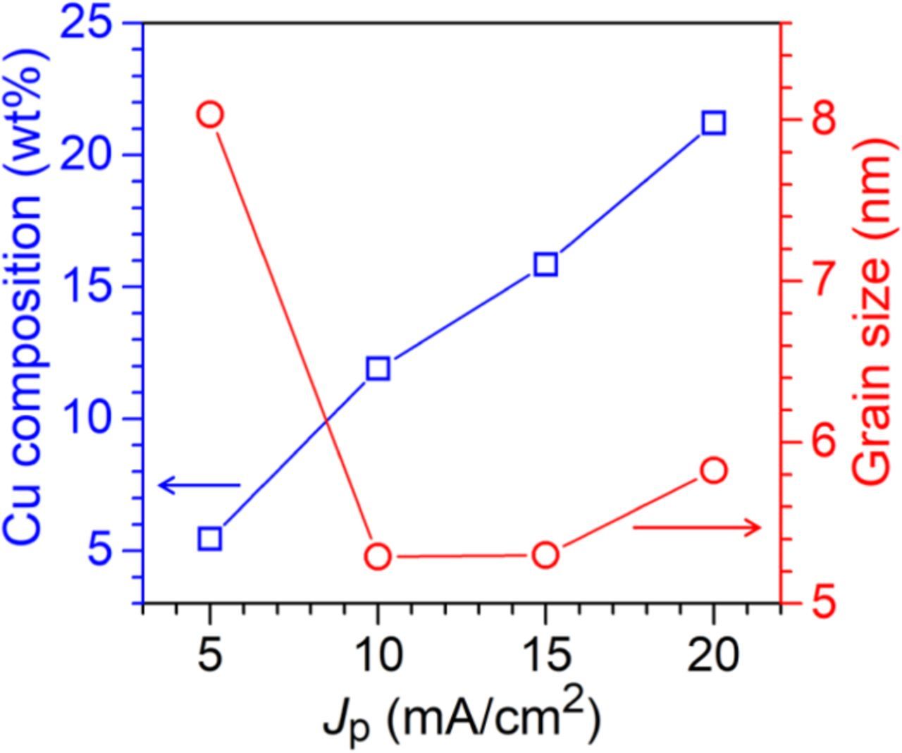
Figure 2. Plots of the Jp versus the dg and Cu composition.
Effect of current off-time
Effects of the toff on crystal structure and alloy composition of the Au–Cu alloys are discussed in this section. Fig. 3 shows XRD patterns of the Au–Cu alloys electrodeposited at the Jp of 20 mA/cm2 and the toff varied from 20 to 120 ms. Similar to Fig. 1, all the XRD patterns showed the fcc reflections, and no other diffraction peaks were observed. The major (111) peak gradually shifted from 2θ = 40.2° to 38.8° when the toff increased from 20 to 120 ms, which indicate a decrease in the wCu. It is known that the toff plays an important role in controlling the alloy composition due to the galvanic displacement reaction occurred on the substrate surface.17,27–29 During the off-time period, nobler metals continue to be deposited on the substrate surface and less noble metals on the substrate surface would be oxidized and dissolved away. The displacement reaction leads to a decrease in concentration of the less noble component in the alloy. In the present Au–Cu system, the standard reaction potential of Au is more positive than Cu, hence the nobleness of Au is higher. Therefore, the displacement reaction occurred during the off-time period would cause a decrease in wCu of the Au–Cu alloy, which is consistent with the lattice swelling observed from the XRD results.
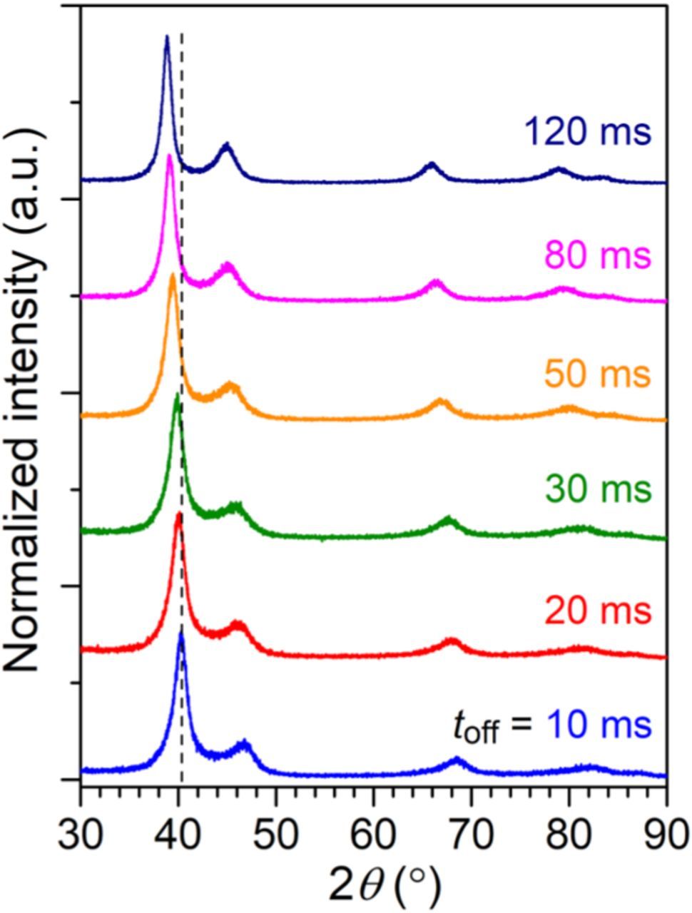
Figure 3. XRD patterns of the Au–Cu alloys electrodeposited at the Jp of 20 mA/cm2 with the toff varied from 10 to 120 ms. The ton was fixed at 10 ms. The vertical dash line indicates center line of the (111) diffraction peak in the toff of 10 ms sample.
Dependence of the wCu on the toff at Jp varied from 10 to 60 mA/cm2 is shown in Fig. 4a. Several trends were observed as the Jp and the toff changed. At first, a decreases in the wCu was observed as the toff increased at all the Jp. The results corresponded well with those observed from the XRD patterns, which more Cu was replaced by Au as the toff increased. Secondly, decreasing rate of the wCu as the toff increased showed a transition from high to low as indicated by the change in slope of the curves in Fig. 4a. The Jp of 50 mA/cm2 curve indicated this point clearly. wCu of the Au–Cu alloy showed a steep decrease from a short toff to toff of 240 ms, and the slop became less steep at a toff longer than 240 ms. The slope is suggested to be related to the displacement reaction rate or dissolution rate of Cu component in the Au–Cu alloy, which a steep slope indicates a high Cu dissolution rate. Again, the result is expected since the Cu dissolution rate is directly related to concentration of Cu component at surface of the film, and the Cu concentration is higher at the moment when the electrodeposition just entered the off-time period. Then the Cu concentration gradually decreases and leads to a lower Cu dissolution rate. Thirdly, the wCu decreasing rate was slowed down as the Jp increased. The evidence can be clearly seen in the Jp of 20 mA/cm2 and Jp of 60 mA/cm2 cases. The wCu decreased from 15.9 to 6.8 wt% when the toff was increased from 30 to 100 ms in the case of Jp of 20 mA/cm2. A much longer toff was required, from 290 to 590 ms, for the wCu to decrease from 16.0 to 7.0 wt% in the case of Jp of 60 mA/cm2. The alloys electrodeposited at higher Jp contain higher wCu. Although the dissolution rate is highly dependent on the Cu concentration, but diffusion of Cu2+ away from surface of the substrate and Au+ from the bulk to the reaction site could also affect the dissolution rate. Hence, a longer toff is needed to reach the same wCu when the Jp is high.
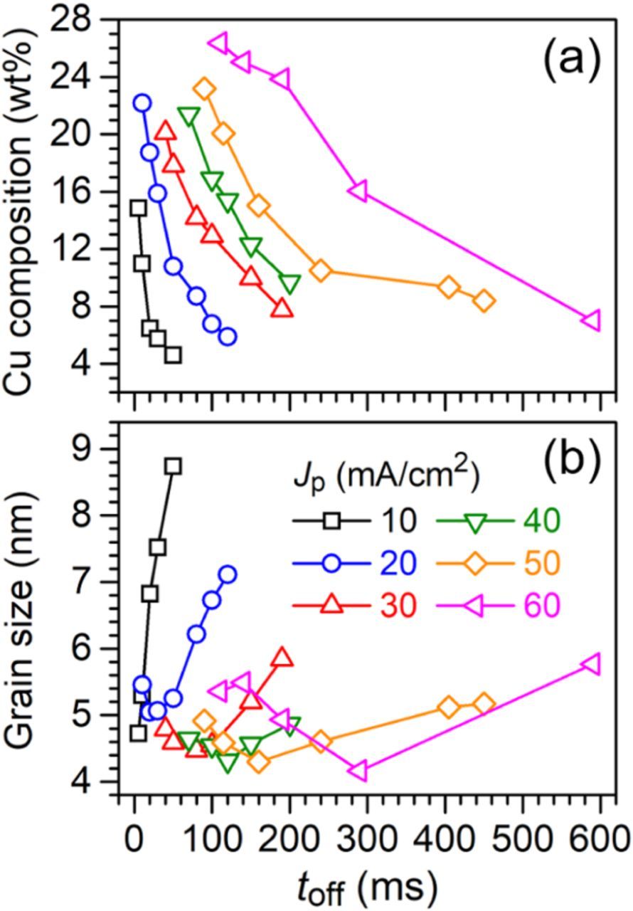
Figure 4. Plots of the toff versus the dg and Cu composition.
Effects of the toff on the dg showed similar trends at various Jp, which the dg initially decreased to a minimum value of ca. 4.40 nm and then the dg increased when the toff increased, as shown in Fig. 4b. The displacement reaction occurred during the off-time period can initiate re-arrangement of atoms in the alloy, which could induce nucleation or grain growth of the reduced metals in the alloy. Driving force of the re-arrangement is dependent on the dissolution rate. When the driving force is high, the re-arrangement is more vigorous and nucleation is induced. As shown in Figs. 4a and 4b, the dg reduced with a decrease in the wCu until the wCu reached ca. 15 wt%. On the other hand, the re-arrangement is less vigorous, and grain growth is favored when the wCu is low. This is why grain coarsening was observed when the wCu was lower than ca. 15 wt% as the toff increased.
As a result, a wide wCu ranging from 3.5 to 26.7 wt% was attained by adjusting either or both the Jp and the toff. In addition, the critical point observed at the wCu of ca.15 wt% indicated the dg was interrelated to the alloy composition. Fig. 5 shows the dg as a function of the wCu. The wCu and the dg followed a monotonic relationship. Similar behavior was reported in other PC electrodeposited alloys.29–31 When compared to the DC electrodeposited Au–Cu (square symbols),20 the DC electrodeposited Au–Cu also showed the same monotonic relationship. Furthermore, as shown in Fig. 5, the PC electrodeposition allows fabrication of Au–Cu alloys with a wider range of the wCu and a much finer dg than those of the DC electrodeposition, which are both advantageous for applications in movable micro-components.
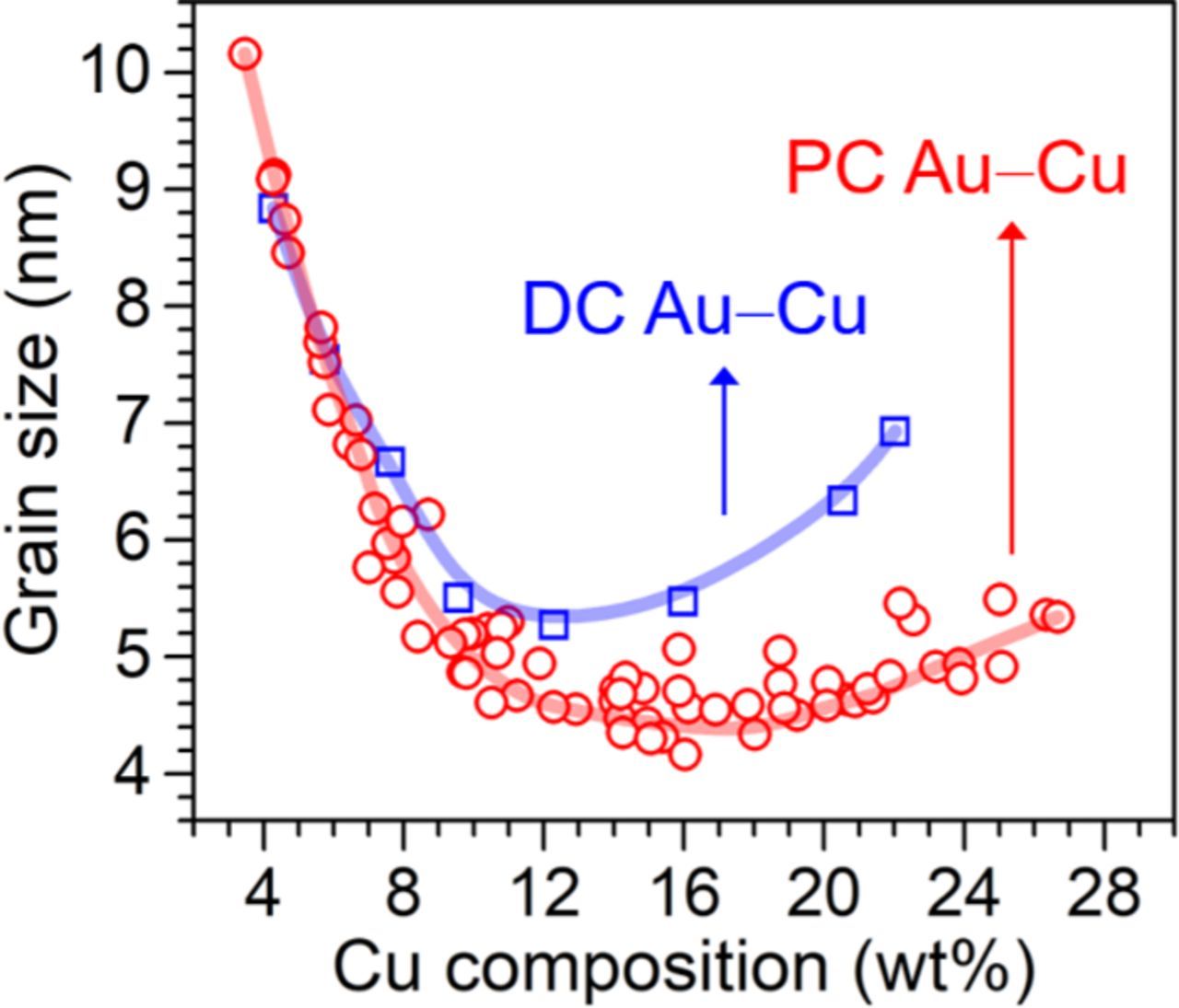
Figure 5. A plot showing relationships between the grain size and composition of Au–Cu alloys electrodeposited with various Jp and toff.
Morphology of Au–Cu alloys
Effects of the PC electrodeposition parameters on morphology of the Au–Cu films were observed by the SEM as shown in Fig. 6. Overview of the Au–Cu alloys electrodeposited at the Jp of 15 mA/cm2 showed bright surfaces when the toff was between 20 to 50 ms. From Fig. 6a, the alloy film electrodeposited at the toff of 20 ms showed pebble-like structures, and size of the pebble-like structures shrank gradually as the toff increased to 50 ms as shown in Figs. 6b and 6c. The surface became dull when the toff was increased to 100 ms, and the pebble-like structures were still observed as shown in Fig. 6d. When a lower Jp at 5 mA/cm2 was used, two alloy films deposited at the toff of 30 and 100 ms both showed dull surface. Size of the pebble-like structures increased as the toff increased to 100 ms (Fig. 6f). The surface condition became very rough when the Jp was increased to 20 mA/cm2. As shown in Fig. 6g, the alloy film deposited at the Jp of 20 mA/cm2 and the toff of 20 ms showed large agglomerates of colony-like clusters, and dull surface was observed. Then the surface became bright, and size of the pebble-like structures decreased as the toff increased to 50 ms, shown in Fig. 6h. An interesting conclusion could be made here, which Au–Cu alloys with similar surface morphology and similar wCu could be fabricated using different pulse parameters (Fig. 6b: Jp = 15 mA/cm2, toff = 30 ms; Fig. 6h: Jp = 20 mA/cm2, toff = 50 ms). This result demonstrated that not only the dg but also the surface morphology was interrelated to the wCu. The morphology, composition, dg, and electrodeposition parameters of the Au–Cu alloys are summarized in Table II.
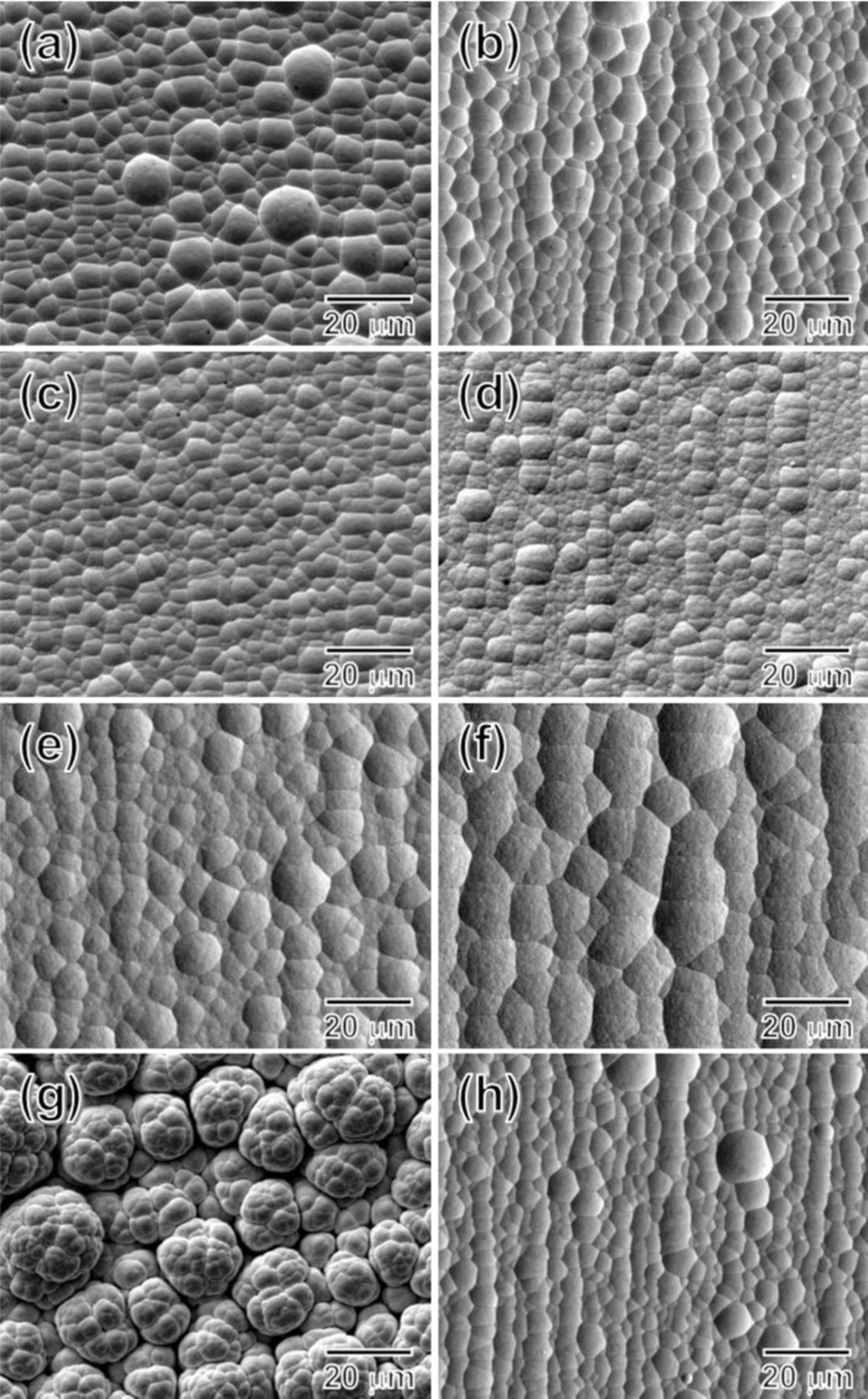
Figure 6. SEM micrographs of the Au–Cu alloy thick films. The alloys electrodeposited at the Jp of 15 mA/cm2 with the toff of (a) 20 ms, (b) 30 ms, (c) 50 ms, and (d) 100 ms; Jp of 5 mA/cm2 with (e) 30 ms and (f) 100 ms; Jp of 20 mA/cm2 with (g) 20 ms and (h) 50 ms. The ton is fixed at 10 ms.
Table II. A summary of pulse parameters, wCu, dg, and morphology of the Au–Cu alloys presented in Fig. 6.
| Jp, mA/cm2 | toff, ms | wCu, wt% | dg, nm | Morphology |
|---|---|---|---|---|
| 20 | 20 | 21.9 | 4.83 | Colony-like clusters and dull surface |
| 50 | 14.2 | 4.68 | Pebble structure and bright surface | |
| 15 | 20 | 15.9 | 4.71 | Pebble structure and bright surface |
| 30 | 14.3 | 4.82 | Pebble structure and bright surface | |
| 50 | 11.9 | 4.94 | Pebble structure and bright surface | |
| 100 | 7.9 | 6.16 | Pebble structure and dull surface | |
| 5 | 30 | 6.6 | 7.03 | Pebble structure and dull surface |
| 100 | 4.3 | 9.09 | Pebble structure and dull surface |
Effects of the Jp and the toff on the morphology and the wCu are summarized and illustrated in Fig. 7. In general, roughness of the surface is affected by the current density applied, and smoothness of the surface is related to the displacement reaction, i.e., dissolution of the Cu component in the Au–Cu alloy. In other words, an increase in the Jp leads to roughening of the surface, and promotion of the displacement reaction causes smoothening of the surface. For example, when a high Jp and a short toff are applied, a rough surface would be formed during the on-time period because of the high Jp, and the smoothening effect caused by the displacement reaction would be insufficient because of the short toff. In this case, a rough surface condition is obtained as shown in Fig. 6g. When a high Jp and a long toff are applied, although the high Jp would give a rough surface, but with a long enough toff, the displacement reaction could cause enough smoothening effect to produce a smooth surface. On the other hand, when a low Jp is used, the surface would be less rough than the one using a high Jp. However, the wCu is low when a low Jp is used, and this limits the displacement reaction, that is the surface smoothening effect. As observed in the alloys electrodeposited at the Jp = 5 mA/cm2 shown in Figs. 6e and 6f, the surface condition did not become smoother as the toff increased from 30 to 100 ms.
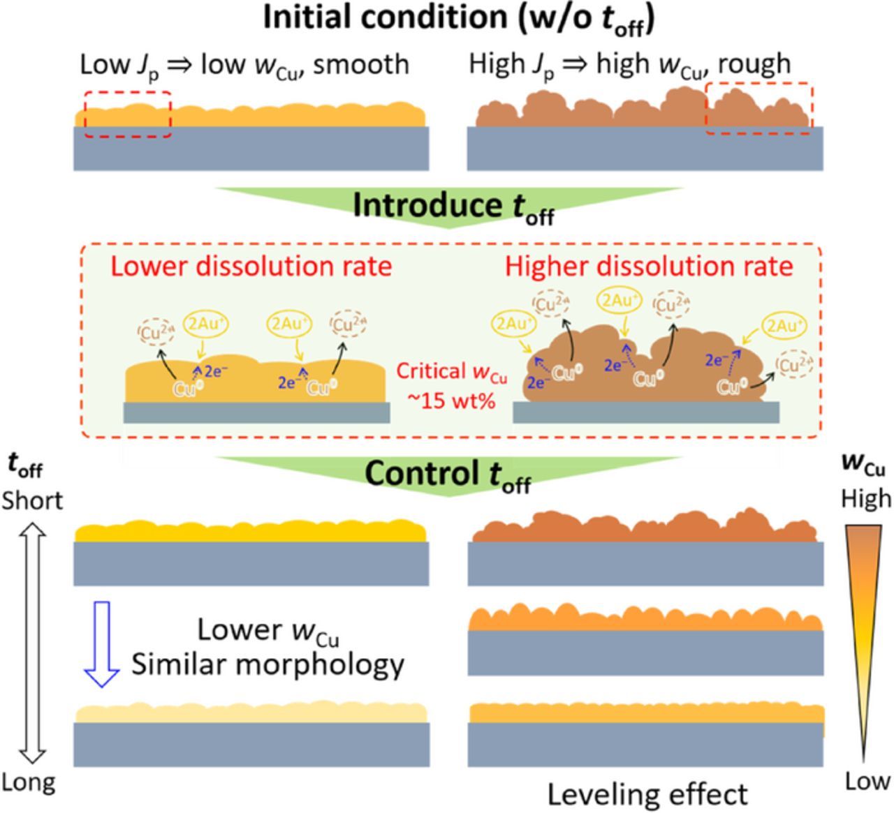
Figure 7. Illustration of the morphology change with the pulse electrodeposition parameters.
Micro-mechanical properties
Micro-mechanical properties of the PC electrodeposited Au–Cu alloys were evaluated by micro-compression tests to demonstrate the potential for applications in micro-electronic devices. The micro-pillars were fabricated from the thick Au–Cu films by FIB, and the wCu of each pillar was 21.9 wt%, 14.2 wt%, 7.9 wt%, and 4.3 wt%, respectively. Fig. 8 shows SIM images of the Au–Cu alloy micro-pillars before and after the micro-compression tests. For the wCu of 21.9 wt% pillar (Figs. 8a and 8b), the surfaces showed clear boundaries originating from the large agglomerates observed in Fig. 6g. After the compression test, brittle fracture was observed as shown in Fig. 8b, which is suggested to be induced by the cracks along the agglomerate boundaries. As the wCu decreased to 14.2 wt% (Figs. 8c and 8d), the typically polycrystalline deformation (barrel-shape)24,32 was observed. The micro-pillars containing lower wCu (wCu = 7.9 wt% in Figs. 8e and 8f and 4.3 wt% in Figs. 8g and 8h) also exhibited the same barrel-shape deformation. The large agglomerates and the brittle fracture were also observed in the DC Au–Cu alloys electrodeposited using a high current density, which the brittle fracture was observed when the wCu was higher than 20 wt%.

Figure 8. SIM micrographs of the Au–Cu alloy micro-pillars (a–d) before and (e–f) after the micro-compression tests. The micro-pillars were fabricated from the thick films with the wCu of (a, e) 21.9 at%, (b, f) 14.2 at%, (c, g) 7.9 at%, and (d, h) 4.3 at%.
Engineering strain-stress (SS) curves obtained from the micro-compression tests are shown in Fig. 9. The σy was estimated from the 0.2% offset line of the elastic deformation region.33 The wCu of 21.9 wt% and 14.2 wt% micro-pillars showed almost the same σy of 1.36 and 1.38 GPa, respectively. However, the subsequent flow stress behaviors were different between the two pillars, which is attributed to the difference in the deformation behaviors shown in Figs. 8b and 8d. The brittle fracture in the wCu of 21.9 wt% micro-pillar lead to the stagnant and trembling flow stress. In contrast, the flow stress continuously increased after the yielding region for the wCu = 14.2 wt% micro-pillar, which is a result of the barrel-shape deformation. The micro-pillars with lower wCu (7.9 wt% and 4.3 wt%) showed similar SS curves as the wCu of 14.2 wt% micro-pillar but lower σy of 1.06 GPa and 0.90 GPa, respectively.

Figure 9. Engineering SS curves of the micro-pillars containing the wCu of (a) 21.9 at%, (b) 14.2 at%, (c) 7.9 at%, and (d) 4.3 at%. The yield strength (σy) is determined by the cross-point of the SS curve and the 0.2% offset line of the elastic deformation region. The σy is marked by a horizontal bar.
After all, the σy ranged from 0.90 to 1.38 GPa in the PC electrodeposited Au–Cu micro-pillars are all higher than that of pure Au, which can be understood as synergistic effects of the grain boundary strengthening5 and the solid solution strengthening mechanisms.9,10 Based on the grain boundary strengthening mechanism, the strength of metallic materials is proportional to reciprocal square root of the dg. This relationship is known as the Hall-Petch relationship.5 On the other hand, the solid solution strengthening comes from the restriction of dislocation movement due to the interaction between dislocation and solute atoms9,10 A number of theories for solid solution strengthening are proposed to show that the strength is proportional to the solute concentration with order of 1/29 or 2/3,10 which is dependent on the solute concentration. It is worth noticing that the highest σy at 1.38 GPa obtained in the PC electrodeposited Au–Cu micro-pillar is higher than that of DC electrodeposited micro-pillar with the same wCu (σy = 1.15 GPa),20 which demonstrates the capability to further refine the dg and enhance the strength by pulse current electrodeposition.
Conclusions
In this study, effects of the pulse current parameters on the alloy composition, dg, surface morphology, and micro-mechanical property of the Au–Cu alloys were investigated. A wide copper concentration in the Au–Cu alloys ranging from 3.5 to 26.7 wt% was obtained. An increase in the wCu was observed by using either or both of a high pulsed current density and a short current off-time. The smallest dg of ca. 4.40 nm was achieved in films having the wCu ranged from 13.0 to 16.0 wt%. Grain refinement was achieved with a high Jp, and promoting the displacement reaction could also reduce the dg. A high Jp resulted roughening of the surface, and enhancing the displacement reaction lead to a surface smoothening effect. Deformation behavior of the Au–Cu micro-pillar was affected by the wCu, which brittle fraction was observed when the wCu was higher than 20 wt%. An ultrahigh σy at 1.38 GPa was obtained in the micro-pillar having the wCu of 14.2 wt% and the dg of 4.68 nm, which is a result of synergistic effects of the grain boundary strengthening and solid solution strengthening mechanisms. In conclusion, this study demonstrated the simplicity (by the pulse current electrodeposition) and the versatility in controlling properties of the Au–Cu alloys for applications in design and fabrication of micro-components in micro-electronic devices.
Acknowledgment
This work is supported by the CREST Project (#14531864) operated by the Japan Science and Technology Agency (JST) and by the Grant-in-Aid for Scientific Research (S) (JSPS KAKENHI Grant number 26220907).
ORCID
Haochun Tang 0000-0001-9258-6368
Tso-Fu Mark Chang 0000-0003-0221-8882