Abstract
The emergence of efficient solid state light emitters was the result of the remarkable breakthroughs in the late 1980s and early 1990s in GaN-based materials and light emitting diodes. Over the past two decades, the continued progress in blue LED efficiency resulted in a revolution in lighting. While the basic physics of nitrides LEDs operation are well understood, nitride LEDs have still open questions, and their reaching physical limits at all wavelengths still raises major challenges.
Export citation and abstract BibTeX RIS

This is an open access article distributed under the terms of the Creative Commons Attribution 4.0 License (CC BY, http://creativecommons.org/licenses/by/4.0/), which permits unrestricted reuse of the work in any medium, provided the original work is properly cited.
Lighting has had a great historic importance and did put a continuing demand on energy resources, despite the huge progress in efficiencies throughout centuries (Fig. 1a). Basically, every new energy source was first put to use to realize better, more efficient lighting (Fig. 1b). As shown in Fig. 1a, lighting sources made enormous progress since the early 19th century, and then improved fifty-fold from 1900–1950 with improvements in incandescent bulbs and then five to ten-fold with the introduction of fluorescent lighting in 1950. Today ∼15% of electricity is used for lighting.
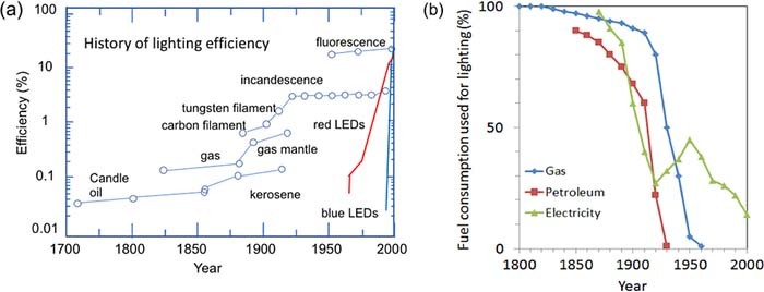
Figure 1. (a) Evolution of light source efficiency for different technologies (after Ref. 1); (b) fraction of energy used for lighting for new energy sources (after Ref. 2). Note the marked decrease in electricity use for lighting in 1950 which coincides with the introduction of the fluorescent light.
Beyond "classic" light sources, the direct conversion of electricity to light in semiconductors had a few (very) early pioneers, but efforts started really in the 1950s with the advent of both the theoretical understanding and the development of the tools of semiconductors. The physics of semiconductors and devices was built on the appearance of high purity semiconductors, on the understanding of their properties, on the mastering metal-semiconductor contacts, on advanced growth techniques, thus allowing for the develop of alloys and heterostructures. Green, red and infrared (IR) light emitting diodes (LEDs) quickly appeared. As early as 1962 the internal quantum efficiency (IQE) of IR LEDs approached 100% and the efficiency of visible LEDs was a few percent around the same time. Efficient blue LEDs remained an elusive goal for a long time, seemingly impossible to reach relying on "conventional wisdom."
We outline the ingredients that enabled LED-based lighting breakthrough through high performance blue nitride LEDs, despite discouraging early results. Major advances were growth of device quality GaN epitaxial layers and GaN-based alloys, heterostructures and quantum wells (QWs) and p-type doping, which led to the award of the 2014 Physics Nobel prize to Isamu Akasaki, Hiroshi Amano and Shuji Nakamura.
There was much progress in understanding the operation of nitride-based LEDs, explaining in turn: (i) the origin of the high IQE, despite the "unreasonably" high dislocation density; (ii) the origin of decreasing IQE with increasing current (the current "droop"); (iii) the cause of decreasing efficiency for increasing emission wavelengths beyond blue (e.g., green or longer emission - the "green gap"); (iv) the excellent reliability of nitride LEDs despite their operating with energetic visible photons, contrary to conventional wisdom which suggests increased defects-assisted motion due to the energy released to the lattice by non-radiative recombination of high energy electron-hole pairs.
The short review is organized as follows: we will first revisit LED history for two reasons: first, a number of early LED pioneers will be forgotten as the story of LEDs is rewritten without understanding the early history. Additionally, many aspects of LEDs are now being taken for granted, for instance that indirect gap semiconductors cannot yield reasonably efficient LEDs. The other is that a number of basic concepts date back long ago and get revived, such as the tentative revival of incandescent lamps through wavelength selective surfaces which would improve their efficiency3–7 or the possibility of wall plug efficiency (WPE) >100% (see below). We will then discuss the various components that resulted in high efficiency of nitride LEDs. We will emphasize our present understanding of droop as due to inter-band Auger recombination and the impact of alloy disorder on materials and device properties. We end by the search for WPE >100% efficiency which is enabled by thermal pumping of carriers.
The Early History of Visible LEDs
"Prehistory": LEDs before semiconductor theory
Solid state light (SSL) emitters were discovered by accident: at the beginning of the 20th century, the leading driving technology was that of radio communications and broadcasting. The emitter and receiver technologies were very primitive and erratic (spark gap discharge emitters ("Hertz oscillators") and "coherer" receivers8–10).
Solid state device solutions for emitters and receivers were actively pursued and a leading technology was the metal point contact ("cat whisker") demodulator based on a metal tip contacting a piece of galena (PbS), invented in 1898 by Braun,9 acting as what we now know as a Schottky diode rectifier. It was the basis of the most popular radio receiving systems until the mid '1920s. As its operation was erratic due to the fluctuating tip-galena contact, these detectors were replaced in the 1920s and 1930s by the much more reproducible vacuum tubes. These in turn were replaced by solid state rectifiers for radar during World War II with metal deposited diodes that allowed reaching higher frequencies and improved directionality of the microwave radiation (for history see Hoddeson11). Amplifier vacuum tubes were later replaced by transistors in the 1950s and 1960s.
In the course of his rectifiers studies using SiC, Round (working on radio research at the Marconi company) observed in 1907 weak electroluminescence (EL) from SiC. He wrote a short note on this result and returned to his work on rectifiers. In his publication of 21 lines Round described the appearance of light emission when injecting current through a SiC crystal, the color varying with the applied voltage, starting at 10 V. However, this work had fallen into oblivion until Round's letter to editor was retrieved in 1969.12
A soviet researcher, Losev (variably also spelled Lossev, Lossew, ... in the literature), independently rediscovered the phenomenon in 1922–192413,14 in his research on rectifiers and oscillators based on ZnO and SiC (for details on Losev's achievements, see Loebner,15 Novikov16 and Zheludev17). Through his systematic studies, Losev discovered two mechanisms of EL, one by direct bias carrier injection in the semiconductor, as done today in LEDs (type II luminescence in Losev's terms), the other by excitation of the semiconductor under high reverse bias voltage (termed type I luminescence).18 We understand now that these metal-semiconductor emitters operated through carrier injection under forward or reverse biasing of metal-semiconductor contacts (Fig. 2). Amazingly, in 1928 he linked the emission wavelength with the theory of quanta, as he observed that under optimal observation conditions the emission of light quanta of energy hν occurred when the applied voltage V was such that qV ≅ hν.19 As the band theory of insulators and semiconductors did not yet exist,20 he relied on the analogy with the phenomenon of bremsstrahlung of electrons accelerated under a voltage V in vacuum. Entering a solid, they lose their kinetic energy qV as X-rays when deflected by nuclei, the most energetic X-rays having an energy hν = qV. As we now know, electrons accelerated in solids suffer very efficient energy relaxation by phonons before reaching a kinetic energy larger than phonon energies. Losev, in at least one instance,21 also observed p-n junction behavior, although not identified as such, as p and n doping phenomena were unknown at the time.
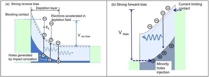
Figure 2. Schematics of the modern explanation of Losev's type-I (a) and II EL (b) in case of a metal n-type semiconductor injecting contact. (a) strong negative bias applied through the contact, which acts as a blocking contact, regulating the injected current. Due to the high accelerating field in the depletion layer, electrons reach a kinetic energy larger than the bandgap, allowing electron–hole pairs to be generated by impact ionization. These electron–hole pairs with energies near the band edges can then recombine radiatively by emitting light; (b): under strong forward bias, minority holes are injected into the n-type semiconductor, recombining with electrons by emitting light. To avoid strong electron (majority carriers) current, electrons are injected by a current-limiting Schottky contact.
EL developed from 1936 on another track, following the discovery by Destriau of the effect that bears his name, the electroluminescence of zinc sulfide (ZnS) powder in an insulating matrix subjected to strong alternating electric field (applied voltage of the order of kV at least in Destriau's original paper, later tens of volts).22 It should be noted that this discovery was also serendipitous: Destriau was looking for better scintillation materials for measurements of radioactive decay, hence the title and main focus of his paper: Research on Scintillations of ZnS under X Rays. His search for the possible excitation of luminescence by electric fields came from the tentative explanation of the scintillation phenomenon as due to the excitation of ZnS by the intense internal electric fields produced by the ionization of light emitting centers through α particles. Destriau's phenomenon in powders is equivalent to Losev's type I process in crystals. Destriau later quoted Losev's work on silicon carbide as the first evidence of electroluminescence of solid bodies. The advantage of the "Destriau" effect lies in its simplicity of implementation with ZnS powder and a binder placed between two transparent conductive plates. It thus generated much research from the 1930s to the 1970s as it was a path to long sought flat panel displays23,24 [To emphasize the predominance of high-field electroluminescence in the post-World War II era, see the remarkable introduction by Dean to his masterful 1969 review of electroluminescence,25 reproduced in Weisbuch26]. The simplicity of manufacture, not requiring high quality crystals, however, has inherent drawbacks: the materials were poorly controlled, had random properties, aged poorly, had a low conversion efficiency, which failed to appreciably improve despite the important research efforts.23,27 Destriau himself recognized in 195528 that only type II electroluminescence, i.e. carrier injection in a semiconductor junction, could deliver the efficiency required for lighting applications. The comparison between high-field EL and carrier injection in p-n junctions was carried in details by Fischer29 and Dean.30
The p-n theory of electron-hole injection: semiconductor properties, device concepts, mechanisms, ... the "modern" past
The path to efficient LED operation was established in the 1951 paper by Lehovec et al.31 [for a fascinating biography of Lehovec, see Lojek32] who explained the operation of blue SiC LEDs through the injection of minority carriers in the depleted zone of a p-n junction where they recombine radiatively. They referenced in great details the pioneering work of Losev.
In a second paper, Lehovec33 also tackled the relationship between applied voltage and photon energy, as previously observed by Losev.19 Lehovec of course related the photon energy to the SiC bandgap energy, but he also noted that photons could be emitted when the voltage was less than the equivalent photon voltage Vphot as defined by Vphot = hν/q, meaning that the energy supplied per electron-hole pair by the power source was less than the emitted photon energy. He correctly conjectured that the energy carried out by the photon in excess of that supplied by the power source would be due to thermal energy supplied by the lattice (§3.1 presents the possibility of LEDs with WPE >100%). On the other hand, some LEDs operate at voltages significantly larger than Vphot. This is then a source of heating of the device and a WPE loss mechanism. Over time, this p-n junction mechanism for light emission, improved by the use of heterostructures, has proven superior to all other injection mechanisms, such as injection from metal contacts (Metal-Insulator Semiconductor (MIS) structures for instance). The injection efficiency (IE) of carriers in the active region is near unity and carriers can be injected with little excess energy compared to the photon energy Vphot.
After Lehovec's work came the choice between direct or indirect gap semiconductors (SCs). Contrary to a wide belief, the case was not so clear-cut in the 1950s and 1960s. The lower IQE of intrinsic indirect bandgap SCs could be vastly improved by the use of deep impurities which allowed quasi-direct transitions thanks to the k-extension of their localized wavefunctions.26,34 In addition, at the time, the available homo-structures p-n junction could not be controllably grown and thus the junction was buried a few microns deep below the surface of devices. The emitted light from direct gap SCs was then strongly reabsorbed (the situation of today's UV nitride-based LEDs due to the use of a top p-GaN contact layer) and the EQE suffered from light extraction efficiencies (LEEs) in the few % range compared with 30% for indirect bandgap LEDs. Therefore, for a long time, direct and indirect bandgap LEDs coexisted in the red wavelength region, whereas yellow-green-blue LEDs where often based on GaP materials (see Table II in Ref. 26).
Table II. Summary of the sources of optical losses in high LEE LED designs (see LED geometries and parameters in appendices of ref. 132): the high power PSS design corresponds to standard LED operation, while the advanced low power PSS optimizes the design for low current operation. The rightmost column calculates the relative change (Δ) in absorption in the low loss design compared with the reference design for each material in the epitaxy and package.132
| Material | Loss in the Reference Design (%) | Loss in the Low Loss Design (%) | Δ |
|---|---|---|---|
| ITO | 7.1 | 0.98 | −86% |
| p-GaN | 0.96 | 0.92 | −4% |
| n-GaN | 0.74 | 0.76 | +3% |
| UID GaN Buffer | 0.26 | 0.26 | 0% |
| Sapphire Substrate | 0.25 | 0.38 | +52% |
| p-metal | 5.5 | 0.58 | −89% |
| n-metal | 1.0 | 0.36 | −64% |
| Rear Mirror | 3.6 | 0.66 | −82% |
| Gold Wire Bonds | 1.3 | 0.89 | −32% |
| Total Losses | ∼21% | ∼6% | |
| Total Extraction Efficiency | ∼79% | ∼94% |
The breakthrough came with the advent of double-heterostructures (DHs) where the active material has a smaller bandgap than the surrounding layers and thus little or no light is reabsorbed. The main structures pursued in the 1970s and 1980s (shown in Fig. 3) were based on the AlAs, GaAs and their alloys (AlxGa1-x)As (referred to as AlGaAs) since these materials are lattice–matched, allowing high-quality epitaxial growth, and GaAs substrates were available. The wavelength range was however restricted to the red-infrared spectral region. Progress went along with improving growth techniques.35,36
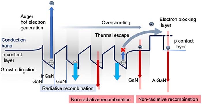
Figure 4. Schematics of electron injection and recombination mechanisms in a nitride heterostructure LED.
The search for shorter wavelength LEDs started in the early 1960s. It was clear that SiC would not lead to efficiencies similar to those of III-V materials. Many compounds and their alloys were studied including those with constituent elements from columns II, III, IV, V and VI of the periodic table. For a long time, II-VIs appeared the most promising due to the availability of substrates and the ease of growth. They however are plagued with rapid degradation under operation.39–42
Nitrides were investigated starting in the early 1960s.43,44 They encountered many growth issues (lack of proper substrate with lattice matching) and the difficulty to obtain p-doping.45–47 In view of these difficulties, the interests of companies switched to other more promising and growing fields such as GaP-based visible LEDs (Philips), GaAsP (GE/Monsanto), and the very important field at the time of telecommunications IR lasers (Bell laboratories, RCA).48 The rest is history as the mismatched growth and doping challenges where solved by Akasaki, Amano and Nakamura.
Modern Development of Visible LEDs (i.e. Materials Systems used Today)
Moving on to modern LEDs based on group III nitride materials (thus omitting a discussion of red LEDs based on the AlInGAP materials system), we will present the various aspects of the efficiency of nitride LEDs, with some focus on a few recent topics beyond the contents of excellent literature chapters in, e.g..49,50
The components of efficiency (Fig. 4)
The efficiency of LEDs (lumens out/electrical power in) is mainly the product of five terms:
- the electrical efficiency, ηEE, mainly associated with Ohmic or contact losses, which represents the fraction of electrical power supplied to injected e-h pairs in the LED active volume; as the energy of e-h pairs qVbias transforms into photons of energy hν, ηEE can be rewritten as hν/qVbias.
- the injection efficiency IE, ηIE, which describes the fraction of injected current into the active, light-emitting region;
- the internal quantum efficiency IQE, ηIQE which describes the fraction of injected electron-hole pairs which are converted into photons inside the active part of the LED structure;
- the light extraction efficiency LEE, ηLEE which gives the fraction of photons emitted outside the LED to those generated inside;
The product of IE, IQE and LEE of an LED gives the external quantum efficiency, EQE (or ηEQE).
Multiplied by the EE, it gives the wall-plug efficiency WPE, ratio of the generated optical power to the supplied electrical power.
When dealing with lighting sources, mainly white light sources, one considers the luminous efficacy of radiation (LER), given in lumens per optical watt of the emitted light, which represents its efficiency on vision. It is characteristic of the emitted spectrum: a source at the peak of eye sensitivity (555 nm) yields 683 lm/W, but is not white. Multiplying the WPE by the LER yields the luminous efficacy of the LED in lm/W, i.e. the number of lumens per electrical watt supplied (often also called luminous efficiency). Depending on the color quality,51 the maximum LER is in the 300–400 lm/W range.52,53 Adding yellow and red to the spectrum of a cool white light lamp to have a better color rendering of the source reduces its efficacy, lm/W, as these colors have a smaller LER.
The two main approaches to white light generation are the color mixed (cm) lamp associating LEDs of different colors and the phosphor-converted (pc) lamp where white light is obtained by down-converting blue LED light with phosphors.
The present commercial state of the art (2017) is 100lm/W for cm-lamps and 153lm/W for pc-lamps.54 The present lower performance of cm-lamps is due to the low efficiency of green LEDs, giving rise to the so-called green gap. High efficiency green and longer wavelength LEDs should enable to realize white lamp efficiencies of 325 lm/W by using cm assemblies of LEDs with different colors operating at or near their physical limits.54 This is to be compared to the 250 lm/W foreseen54 for the extrapolation of pc-white lamps, where the performance is intrinsically limited by the quantum energy loss (the Stokes shift) of down-converted photons relative to the blue pump photons.
Challenges in measuring EQE, LEE, IQE
It would seem highly useful to measure all parameters that determine efficiency to improve materials and LED designs. This is however a remarkably difficult task (see also David et al.'s paper55).
The WPE and EQE are easily determined from the measurements of the emitted power in an integrating sphere and the applied current and voltage. Then, from the EQE, one can deduce the IQE assuming that ηIE and ηLEE are known: in that case, IQE is just the ratio of EQE to IE x LEE.
We discuss the IE later. Knowing ηLEE requires precise modelling of LEE in well-defined geometries and controlled structures. Spurious effects can occur, such as current crowding due to insufficient current spreading in the top p-GaN layer that causes variation of ηLEE as more light is emitted under contacts (unless using LED designs that avoid light emission under the p-contact). This gives rise to an apparent efficiency droop, not caused here by the IQE droop but by the decrease of the LEE with increased carrier injection.56
The calculation of ηLEE can be performed with reasonable accuracy in two limiting cases: (i) the extraction efficiency is large with LED designs that allow nearly all photons to be extracted, with losses mechanisms accurately measured, calculated or simulated (e.g., GaAs/GaInP double heterostructures which are index matched with ZnSe hemispheres with 96% ηLEE,57 or nitride LEDs with transparent GaN substrate and triangular shaped for optimized side extraction58 with 94% ηLEE); (ii) one uses a well-defined planar geometry, with a structure designed to allow only single pass directly emitted light to escape the LED, still requiring a detailed knowledge of materials parameters.59–61
In modeling electrically injected LEDs, there are additional uncertainties about the power really supplied to the active region (as due for instance to ohmic and contact losses, but this can be however included in the global losses in power efficiency of the LED), and whether the ηIE is strictly unity (see below). One should also take into account that we are describing inhomogeneous device systems with averaged quantities over the whole active region as if they were homogeneous: with changing the injected current, the quantum-confined Stark effect (QCSE) differs between QWs as their relative populations change with carrier injection which affects spectrum, linewidth and their A,B,C coefficients. Additionally, alloy fluctuations effects have to be considered way beyond their effect on the carrier diffusion length as carrier localization also impacts strongly perpendicular transport, and effective SRH, radiative and Auger coefficients.62
The injection efficiency ηIE
As mentioned above, it is widely assumed that ηIE is most often near 100%63 as a number of solutions have been implemented to inject carriers more efficiently and avoid two issues, carrier overshoot and electron carrier leakage in the p-region of the LED's p-n junction. Carrier leakage out of the active region is usually due to thermal activation, which we will call thermal escape from now on to distinguish it from the current leakage due to extrinsic current pathways (dislocation pathways, sidewalls, small parasitic current pathways) in devices. Carrier overshoot,64 i.e. non-capture of the electrons injected from the n-side (see Fig. 4), is avoided by the use of multiple QWs, with electrons overshooting one QW being captured by the subsequent QWs (due to their heavier mass, holes are always captured). Carrier leakage and electron overshoot into the p-GaN layer surrounding the light-emitting QWs is avoided by using wider bandgap (AlGaN) electron blocking layers (EBLs). Detailed experiments conclude to the absence of carrier leakage and overshoot under normal operation circumstances.55
This is supported by 1D simulations (see below), which rely on solving the drift-diffusion (DD) equations, which do show that ηIE is unity up to very large injected currents (several 100's of A/cm2), but this is obtained assuming thermal equilibrium of the carrier distributions, which of course does not account for hot and ballistic electrons. However, other simulation approaches such as Monte-Carlo-based methods65 give a similar result until the applied diode bias significantly exceeds the built-in voltage VBI. Non-equilibrium Green's function (NEGF) computations also conclude to negligible carrier thermal escape or overshoot.66 3D LED modelling including alloy disorder also show that carrier leakage is negligible at LED operating voltages and current densities.67 It seems that commercially available modeling softwares overestimate the voltage applied to the junction, leading to large overshoot currents due to hot electrons accelerated in the high-field associated with sometimes an (unphysical) 5 V bias which greatly exceeds the built-in voltage VBI of GaN-based LED (VBI ≈ 3.2–3.3 V).68 Simulations most often do not include non-ohmic contact and resistive effects, which presents a challenge when making quantitative comparisons with real-world LEDs.
Unfortunately, measurements of ηIE are practically impossible, as modifications of LED structures to change ηIE in a known way will also modify other transport and recombination parameters. When measuring state-of-the-art commercial blue LEDs, one can safely assume that they rely on optimized architectures which indeed have unit ηIE ≈ 1. This is based on state of the art LEDs having EQE above 80%, with LEE above 90% and peak IQE at or above 90%, leaving very little room for a below unity IE.
To illustrate the difficulties of designing and interpreting experiments aiming at characterizing carrier thermal escape and overshoot in IE, in the presence of an EBL, some argue that the injection of minority electrons to the p-side of the LED p-n junction is proof of carrier overshoot/thermal escape. In our opinion, observing such electrons is no proof69,70 since, as stated by Vampola et al.69 in his study of a specially designed LED, "...the mechanism responsible for electron overflow is undetermined ... Both traditional overflow[in our terminology thermal escape] mechanisms and Auger-assisted electron overflow mechanisms are capable of explaining this data". This is because the Auger effect generates hot electrons that can overshoot the EBL (or the QW to p-layer energy difference when no EBL is present), and such electrons cannot be distinguished from "classic" overshoot or thermal escape electrons. Most authors however citing this paper use it as proof of overshoot or thermal escape electrons71,72 (!). ignoring those generated by Auger recombination, and Vampola's cautionary statement (more on the measurements of the electron escape current in the section on droop).
The IQE at low current densities
There has been much speculation about the outstanding properties of nitride materials when compared to other semiconductors, in particular (i) why is the IQE so high with threading dislocation densities on the order of 1–5 × 108 cm−2, way beyond any value which could give a decent IQE in other materials73 ?; (ii) why is degradation under operation so slow, despite large energy release to the lattice during every NR recombination event?
The high IQE at low injection is still incompletely understood. The impact of dislocations is not straightforward as in usual III-Vs. There, dislocations are accompanied by point defects acting as non-radiative (NR) recombination centers which lead to strong NR recombination whenever dislocation density is high. Several effects have been invoked to explain the low activity of dislocations in nitrides. First, the diffusion lengths in active layer, most often alloy QWs, are quite small compared to other materials (although measured values vary substantially),74,75 which makes the capture radius of carriers by dislocations small, eventually smaller than the dislocation separation. This is for instance the case for threading dislocation densities of 108- 109 cm−2 for diffusion lengths in the 100 nm range. This mechanism was invoked very early on when it appeared that a small addition of In to pure GaN QWs increases drastically the EQE.76 It is expected that the compositional fluctuations of the alloys will lead to strong carrier scattering, eventually to carrier localization. It should however be noted that carrier localization through alloy fluctuations have additional effects, such as decreased local radiative recombination coefficient due to in-plane decreased e-h overlap, and increased Auger coefficients. For a discussion of the correlation between Shockley-Read-Hall (SRH), radiative and Auger coefficients see David55,77). It has been also argued that due to the ionicity of the materials, extended defects lead to dangling bond states with energies near the band edges, which make them act as transient carrier traps rather than as NR recombination centres.78 This is quite strongly supported by the fact that LED degradation of IQE is connected to slow increase of point defects density, not to a fast degradation mechanism such as dislocation motion.79
Recent work has demonstrated the impact of pre-active region designs to diminish defects or impurities associated with SRH. A variety of pre-well superlattices (SLs) or QWs have shown beneficial effects (see Haller80).
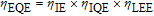
Another possible remedial effect to dislocation activity is the separation of carriers within c-plane InGaN QWs from the majority dislocations, threading dislocations, by the formation of V-shaped pits surrounding the dislocations during growth. Due to the fact that QWs are thinner on the facets of the V-pits as growth is slower than in the c-direction, carriers experience an energy barrier on the path to the NR area around the dislocations which therefore become inactive [Hangleiter81 and references therein]. This hypothesis has recently been given large support from the high EQEs measured for long wavelengths LEDs designed to take advantage of carrier injection from the V-pit facets.82 This high EQE is compounded by the low turn-on voltages of such LEDs which lead to record high WPEs (Fig. 5).
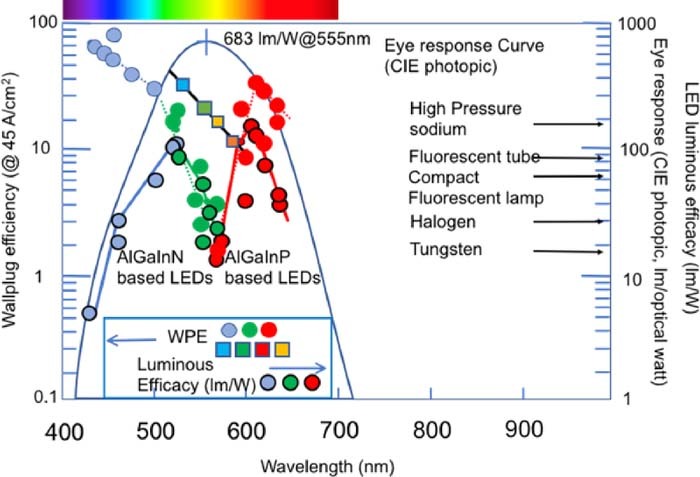
Figure 5. Wall plug efficiency (WPE), luminous efficacy and eye response curve (full line curve) of visible LEDs. Note that the luminous efficacy (lm/W) is the product of the WPE and the eye response, hence violet LEDs have a poor luminous efficacy despite their excellent WPE. The outstanding impact of V-pit injection82 on WPE is shown for LEDs identified with square symbols.
The efficiency at high current densities: droop in nitride LEDs
The main issue in blue LED efficiency is the IQE droop under high driving current densities. While peak IQEs in the 90+% range have been reported, these values are only realized under low current densities on the order of a few A/cm2.
The droop phenomenon is often analyzed through the ABC model of the IQE, where A is the SRH NR recombination coefficient, B is the bimolecular radiative recombination coefficient, and the Cn3 term is a non-linear NR radiative term.
In this ABC model of droop, the injected current in the LED J and IQE are given by:
![Equation ([1])](https://content.cld.iop.org/journals/2162-8777/9/1/016022/revision1/d0003.gif)
![Equation ([2])](https://content.cld.iop.org/journals/2162-8777/9/1/016022/revision1/d0004.gif)
where q is the electron charge, d is the active layer thickness, n is the electron concentration (equal to p), is the injection efficiency. A is usually due to SRH NR recombination mechanism at deep centers, B is the bi-molecular radiative recombination coefficient, C is a higher-order NR recombination mechanism (Fig. 6). These two equations are "reasonably" verified in LEDs,55 but with a very wide range of parameters which all lead to excellent fits (see e.g. the discussion in Ref. 83).
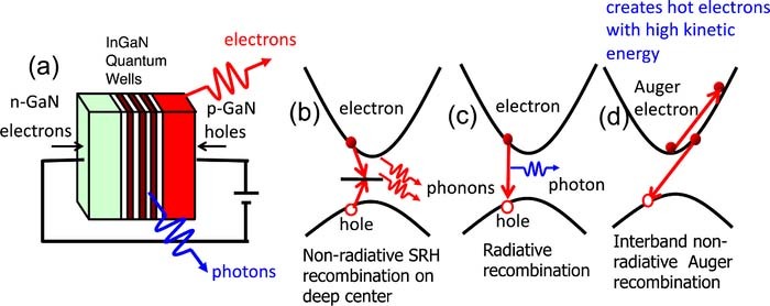
Figure 6. (a): Schematics of an LED under current injection showing the main recombination mechanisms. Electrons and holes recombine radiatively in the active quantum wells by emitting photons.; (b) SRH non-radiative recombination at deep centers; (c) radiative recombination; (d) direct inter-band Auger effect in semiconductors: an electron-hole pair recombines by exciting another electron to high kinetic energy.
There have been long arguments about the physical mechanism at the origin of droop. Before the seminal paper by Shen et al. in 2007,84 the cause for droop was thought to be of extrinsic nature, due to poor injection efficiency or carrier delocalization at increased currents from localized states with high IQE. This state of affairs changed dramatically when Shen et al. announced that droop was due to an intrinsic effect occurring at high carrier density, the Auger effect, through an analysis which introduced the ABC modeling, relying on carrier lifetime changes with carrier density. That observation was the starting point of a huge effort to unambiguously determine the origin of efficiency droop.
At first, disagreement reigned because of theoretical evaluations of the Auger coefficient. Namely, the measured Auger coefficients were several orders of magnitude larger than expected from simple direct 3-body calculations.85 Then, theorists calculated indirect phonon-assisted Auger recombination rates in the 10−31 cm6s−1 range86 while others claimed values in the 10−34 cm6s−1 range, both for direct and indirect Auger transitions.87 Vaxenburg88 found significantly increased direct Auger rates in QWs when compared to bulk ones due to the size and shape of the microscopic confinement potential whereas the radiative recombination coefficient is almost unchanged. Kioupakis et al.86 claim that the Auger and radiative coefficient change similarly with In composition. Bertazzi et al.89 predict strong variations of the direct Auger coefficient with QW thickness, however not taking into account internal electric fields, and also predict a weak Auger coefficient in blue LEDs, and little change for the phonon-assisted Auger effect.
It is now widely accepted that indeed the inter-band Auger recombination mechanism can be theoretically responsible for droop. The main reason for its magnitude being much larger than first expected is due to effects of compositional fluctuations: the localized nature of the electron and hole wavefunctions make the integrals entering the Auger coefficients much larger than for delocalized Bloch wavefunctions. This can be understood as disorder relaxing to some extent the k-conservation rule in the Auger transitions. An additional apparent increase of Auger coefficient is due to the increased local carrier densities in the alloy disorder. The connection between disorder and Auger induced droop is well confirmed experimentally by the absence of droop in PL measurements of GaN QWs which of course are free from alloy disorder.90,91
Experimentally, there was also controversy about the identification of the main droop mechanism, mainly due to using simplified models, such as fitting dependence of light output power on current density to discriminate among the various mechanisms. These measurements only indirectly probe the internal LED physical processes through space, time and energy integrated quantities, not probing in details the microscopic electronic and optical processes. They also treat the A,B, and C coefficients as independent of carrier injection, often neglecting phenomena such as carrier-induced changes in internal electric fields (which change the A, B, C coefficients with injection) and carrier in-plane spatial inhomogeneities (which for instance increase the relative impact of the non-linear processes - for a full analysis see David55). Also, device simulations usually neglect alloy disorder (more below in §4).
Another source of disagreements between experiments is that mechanisms are often measured in academically-grown varied structures, e.g. single QW or DH LEDs, and are possibly being quite different from commercial LEDs and therefore possibly not representing the state of the art, as often apparent from I-V curves.
Finally, PL measurements are in principle very different from EL ones (electrical injection effects are absent). Therefore conclusions from the analysis of pure PL measurements cannot be transposed to the situations encountered in electrically-driven devices because there is no applied bias in PL experiments (and often no diode at all!), injection is homogeneous in all QWs of MQW structures and the electron and hole generation rates are equal. Since PL structures are usually unbiased, there is no possibility of carrier overshoot.
It occurred to us that the best evidence for the generation of hot carriers by the Auger effect would be to measure the electron kinetic energy inside the LED.92 This is possible because the energy distribution of electrons emitted from the surface of an LED into vacuum is the same as it was within the electron emitting materials. We note that this is only approximately true, as some electrons lose energy in the semiconductor before reaching the surface, either through energy relaxation in the bulk or in the so-called band bending region at the surface. However, the kinetic energy of measured emitted electrons can be related to the energy of the electrons within the semiconductor prior to emission, their maximum energy being equal to the maximum electron energy in the material. Low-energy photo-electron emission spectroscopy has widely been used to study electron energies and relaxation mechanisms in semiconductors.93,94
In our experiments on electron emission spectroscopy (EES) from LEDs,92 schematically shown in Fig. 7, instead of photons exciting electrons like in the photoelectric effect, hot electrons are generated in the QWs of a commercial LED operating in forward bias. A substantial fraction of electrons and holes that are injected into the QWs recombine radiatively. However, some injected electrons could escape to the surface p-layer, or can be photo-generated in that p-layer by the LED-generated light. The LED light also generates photoelectrons from the metal contacts.95,96 Finally, at high injection currents, a fraction of the carriers injected into the QWs with the highest carrier density recombine by an Auger process, generating hot electrons.
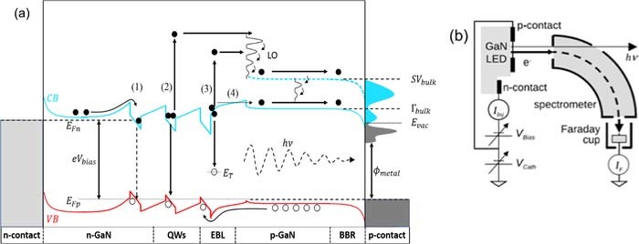
Figure 7. (a) Relevant electron energy levels, transport, recombination mechanisms, and the corresponding electron emission spectrum in a forward biased LED with a cesiated surface yielding negative electron affinity: (1) Radiative recombination; (2) inter-band Auger recombination; (3) TAAR in EBL, and (4) thermal escape (From Ref. 95); (b): schematics of an EES experiment.
All these electrons, with various energies, among which energetic Auger electrons, will travel toward the surface and be emitted into vacuum (Fig. 7, left). Measuring the energy of these electrons should then give evidence of the Auger electrons, provided that some Auger electrons reaching the surface conserve a significant fraction of their high initial energy. Such Auger-generated hot electrons have by now been observed in a wide variety of LED structures from industry and our labs.97,98 They prove the inter-band Auger NR mechanism at high injection for high quality LEDs.
It was thought previously (in particular by us) that transport measurements or integrated optical emission experiments cannot distinguish electron energies. Recently, a novel mixed electrical-optical measurement technique was designed to measure the hot electron current through electrical technique. It is based on the analysis of a small photo-modulated current in forward biased LEDs.99 Under constant applied current, one measures a decrease in junction voltage, which would correspond to a diminished electrically-injected forward current for applied bias below VBI (for which the photo-current would also be in the reverse direction). However, it is a forward photo-current which is observed, meaning that it is due to another cause than equilibrium carrier thermal escape, in that case Auger-generated hot electrons overshooting the EBL. Thus, one can indeed observe hot electron generation by usual optical-electrical excitations.
Other well-designed PL spectroscopy experiments can also trace hot carrier thermal escape generated by the Auger effect in undoped or doped structures. Binder et al.100 have shown hot carrier generation attributed to the Auger effect in a MQW structure containing both UV and green QWs: when exciting green QWs with intense blue light, UV light emission can be observed from the adjacent larger gap QWs due to hot electron transfer associated with the Auger effect. These experiments are however carried out in specially designed nitride PL structures, not in LEDs.
Beyond the inter-band Auger NR mechanism, more Auger processes in nitrides have been recently discovered, such as trap-assisted Auger recombination (TAAR) associated with MBE growth101 or with AlGaN EBLs (mechanism (3) in Fig. 7a)95 or with green-emitting materials.102
For completeness, let us discuss the invoked droop mechanisms other than Auger. Evidence is either based on experiments or modeling. As will be shown, the evidence claimed to originate from experiment is always dependent on modeling the experimental results and is therefore indirect, subject to caution, in particular due to limitations of the ABC data fitting analysis.
Three types of measurements are invoked for justifying thermal escape or overshoot electrons: (i) spectroscopic evidence of electron population in the p-region of the LED, passed the EBL, showing carrier thermal escape from the active region; (ii) presence of photocurrents outside QWs in the photo-pumped structures; (iii) incomplete carrier thermalization in localized states at high currents as revealed by emission spectral shifts.
We discussed above that the presence of electrons in the top p-layer of electrically-injected LEDs is no proof of carrier leakage out of the active region, as it can be due to carrier escape or to Auger-generated hot electrons (Vampola69). The photocurrent issue under photoexcitation has led to conflicting reports. Only the existence of sizeable photocurrents (i.e. comparable to the droop current) under photoexcitation would be a proof of carrier escape or overshoot as the origin of droop. Conversely, the presence of droop under photoexcitation is a major argument of the proponents of Auger mechanism, as giving evidence of droop mechanisms intrinsic to the active region: they argue that this excitation method is supposed to avoid carrier overshoot or escape since no bias is applied. Photocurrents under photoexcitation has been observed by,103 for instance, and then claimed to be a proof of carrier thermal escape or overshoot. In a systematic study, David et al.104 showed that the existence of photocurrent is due to the photovoltaic current at low optical injection, which saturates at high intensities when the photovoltage is high enough to suppress the electric field driving the carrier escape out of the QWs under flatband conditions similar to those existing when an LED is driven beyond the onset bias voltage (the David et al.104 analysis of course follows along the very straightforward understanding of solar cells: the open circuit voltage, VOC, is realized when the drift-based photocurrent equals the diffusion-based diode current. In InGaN MQW solar cells, with epi structures very similar to LEDs, IQEs higher than ∼95% have been realized at low illumination105). Conversely, at high intensities, emitted light can indeed decrease when a reverse bias is applied leading to carrier escape from QWs, proving the origin of the photocurrent as due to field-induced carrier escape. Besides showing that thermal escape is indeed absent from photo-pumped structures under droop conditions, David et al.104 also showed the impact of the EBL to reach high EQEs by suppressing carrier escape or overshoot, the optimum composition being in the 20% Al content range, in good agreement with simulations (see e.g.106). We believe, as industry experts do, that the similar results from EL and PL droop indeed proves that the current droop mechanism at room temperature is due to an internal process within the active QWs, as carrier escape is negligible under photoexcitation of unbiased LED structures.
Thermal droop of nitride LEDs
So far, the analysis of the processes entering the LED efficiency has been done for room temperature. EES measurements have recently been extended to perform the analysis of thermal droop.95 There is a number of thermally-activated processes that could play an important role in the thermal droop of LEDs. The proper identification of the main mechanisms for thermal droop is thus made complicated under electrical injection of carriers, by the simultaneous electrical and optical phenomena coming into play, and their possible inter-relations. For electrical processes, one has to sort out electrical injection in the optically active region, carrier overshooting and carrier escape from that region, ... For optical processes, one has to consider linear, quadratic and third order radiative or NR light recombination or emission processes, carrier-induced NR recombination, ... When trying to understand the thermal evolution of emission efficiency, most often a diminishing one called thermal droop, one has to foresee and measure the temperature-evolution of the various relevant processes. An obvious candidate to explain thermal droop is of course increased thermal escape from the active region. Other mechanisms of thermal droop which have been also invoked are thermally-activated impurity tunneling107 or a temperature-increasing inter-band Auger NR recombination coefficient.108
In a series of experiments aiming at identifying the main mechanism of thermal droop,95 we first identified a new TAAR mechanism associated with defects in an AlGaN EBL in p-n junctions through the emission of hot electron in vacuum. We then use such hot electrons as a signature of electrons reaching these EBL defects in a LED with EBL when the temperature is raised to 130°C, temperature where thermal droop also appears in the light output, while thermal droop increases continuously from room temperature for LEDs with no EBL.95 The experiment thus establishes carrier escape as a major component of thermal droop. Let us remark that in commercial LEDs thermal droop starts at somewhat lower temperatures, so that this value of the onset temperature of thermal droop might be specific to the LED under study.
The robustness of nitride LEDs
The slow degradation of nitride LEDs (and lasers!) under carrier injection is particularly surprising when comparing to the II-VI materials which seemed in the 1980s a better bet due to the availability of decent substrates and good initial quantum efficiency.40 Conventional wisdom was that degradation in light emitters occurs as NR point and line defects are generated in the active layer during LED and laser operation, even more so with high-energy e-h pairs giving visible or UV photons and in presence of strain. The nitride emitters, in contrast with cubic II-VI-based emitters where degradation could occur in matter of minutes (see Itoh et al.109), experience relatively little defect generation and dislocation glide – fortunately as c-plane oriented GaN has no shear stress on the easy dislocation glide planes, c-planes and prismatic m-planes.110 It is not fully understood why point defect generation occur at a very low pace, and why dislocation climb associated with these point defects does not occur. It is speculated that this might be due to the hardness of nitride materials.111
The impact of the internal electric fields in nitrides
The role of the large spontaneous and piezoelectric fields existing in nitrides (in contrast with other semiconductors) is well understood. They lead to a light emission blueshift with increasing drive current density due to the screening of the polarization-related electric fields by injected carriers. What is less obvious is that these fields are not strongly detrimental to the IQE, by diminishing the radiative recombination rate due to the reduced electron-hole wavefunctions overlap. It seems that the NR recombination mechanisms are diminished by the same overlap factor,77,86 which overall should not impact the low current density IQE or the maximum IQE. These fields have however an indirect impact on IQE: since the diminished recombination rates cause an increase in overall carrier lifetime, the optimal carrier density (corresponding to the maximum IQE) is reached at lower current density than if no fields were present. This is at the root of one of the possible solutions to droop by using nitride materials with zero or diminished electric fields in the emitting QWs, grown on nonpolar or semi polar GaN planes.
The light extraction efficiency LEE
LEE has been an issue with LED efficiency since the beginning of light emission of semiconductors.112,113 Due to their high refractive index n ≥ 2.5, only a small fraction of internal emission impinges at angles smaller than the critical angle for total internal reflection (TIR). At a single planar face of a standard nitride LED, extraction efficiency is limited to only ∼ 12%, while propagation in the GaN layers and in the sapphire substrate take the 88% reflected photons by TIR (Fig. 8). Emitting into a dome shaped higher index material like silicone or epoxy only partially solves the problem as no transparent encapsulant material matches the refractive index of semiconductors. As a rule of thumb, extraction will be increased by a factor n2, with n the index of the dome-shaped material relative to air (for which n = 1). Many solutions have been attempted to circumvent the trapping of light inside semiconductors. The simplest solution to this drawback is using LED structures which redirect light beams that underwent TIR in another incidence angle for their next encounter with the semiconductor-air interface. This is the solution offered by geometrical or ray optics, relying on shaped devices or disordered interfaces. Another solution relies on wave optics and optical mode quantization, which be achieved in a number of ways, through microcavities of varied photonic dimensionalities (which include photonic crystals), or simpler interference systems.
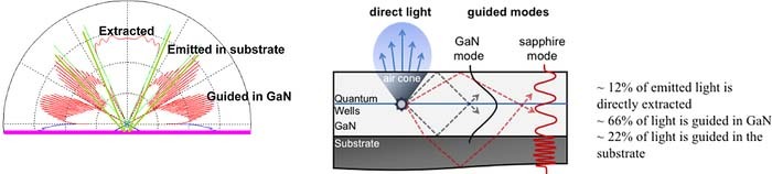
Figure 8. Schematics of light emission and extraction from an emitting QW embedded in a GaN thin film on a sapphire substrate. (left) angular emission diagram. (right) schematics of the modes into which light is emitted: modes directly extracted, modes guided in the GaN layer, modes guided in the sapphire substrate (not shown are modes extracted through the substrate).
Table I shows the various approaches that can be used for high ηLEE. As can be seen, beyond changing directions of light propagation in multiple reflections, some solutions act on the emission source itself, changing the directionality of emission so that more light is concentrated in the escape angle, or controlling/suppressing spontaneous emission and its directionality. Finally, one could at once increase spontaneous emission rate (thereby diminishing the relative importance of NR recombination) and directing emission, as in plasmons/polaritons, concepts not yet demonstrated at high efficiency.
Table I. Opportunities for improved ηLEE and solutions to improve light extraction and efficiency in semiconductor structures. Note that most of the solutions rely on photon mode control and very little on electron quantization (quantum dots). PhC stands for photonic crystals.
| Potential improvement | Concept | Realization | Present state-of-the-art | Challenges |
|---|---|---|---|---|
| Control spectral and spatial emission | - Redistribute spontaneous emission | Planar QW microcavity | Spectral control determined either by beam aperture or linewidth.114,115 | LEE limited to 40%, with optimal mirrors.114–116 |
| - Mode control | Large spectral brightness | |||
| Increase efficiency by control of emission modes | Control & suppress spontaneous emission | Needs 3D optical mode control. | Demonstrated in PL117 | Low power for single emitting area |
| 2D PhC in slab/3D PhC | ||||
| Increase spontaneous emission rate | Rely on Purcell effect by increased local photonic density of states | 3 D microcavity: pillars, photonic crystal | Pillar microcavities well demonstrated – single photon sources118 | Reduced active volume means low power. |
| Plasmons | Plasmon effects seen in PL, no EL device | Requires fine tuning and positioning.120,121 | ||
| Strong coupling-polaritons | Laboratory demos.119 | |||
| Increase light extraction efficiency | Get all rays (geometrical optics) or modes (wave optics) out of material | Change ray direction (chip shaping or surface disorder) or diffract out (PhC) | Surface disorder or growth on patterned substrate. 90+ LEE routine in industry. | 98% + required for 100% WPE.122 |
Improving the directionality of light emission has been widely studied either through the use of microcavities or photonic crystals. Planar microcavities have been shown to have an extraction efficiency limit of ηLEE = 44% into silicone encapsulants in the nitride materials system.116 In conventional III-Vs, a record performance of ηLEE 28% in air has been demonstrated.123 The performance limit is due to waveguided light that is not extracted. Photonic crystals (PhCs) have been used to increase light extraction by diffracting guided modes into air. Quite high extraction efficiencies have been demonstrated including ηLEE = 73% for a high efficiency un-encapsulated surface PhC LED124 and ηLEE 94% for an encapsulated embedded PhC LED.125 Design rules have been defined, such as optimal depth (surface LEDs) or thickness (embedded PhC LEDs), as well a PhC symmetry.126 The main difficulty of PhC LEDs is their delicate required fabrication. Also compared to geometrical optics extraction solutions, light travels much longer in-plane paths in PhC LEDs (typically 40–100 μm)127 compared to only 2–3 roundtrips across the LED thickness for patterned LEDs. Therefore, PhC LEDs are much more sensitive to internal losses than patterned LEDs.
For the sake of completeness, we note that PhCs consisting of a 2D array of periodic holes pierced throughout semiconductor slabs can lead to ultra-high extraction efficiencies of photoluminescence as the slab in-plane optical modes that are not extracted are forbidden to propagate thanks to the photonic bandgap of the PhC, hence avoiding losses.117,128 However, reduction of such structures to practical uses has not been demonstrated.
As mentioned above, the solution for highest ηLEE relies on redirection of light rays, either through surface roughening, or through growth on patterned sapphire substrates (PSS)129 the most widely used solution. A simple and powerful simulation method which encompasses the details of the LED geometry (Figure 9) is provided by ray-racing softwares.130 Such tools facilitate computation of the extraction efficiency of full LED structures, taking into account the materials parameters and the exact geometry of the structure.
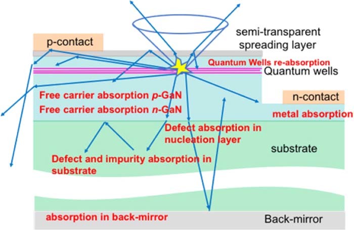
Figure 9. Schematic of showing the main sources of optical losses in LEDs.
Therefore, the different sources of losses can be evaluated (Table II) which in turn provides guidance for new designs for reduced optical loss.
One might wonder what happens if the light extracting features are sufficiently small to require wave analysis instead of geometrical propagation of rays. Full EM computations have been carried out for simple structures by David.131 A comparison of the wave optics vs. optical ray tracing is shown in Fig. 10. It can be seen that the differences in angle-integrated single pass extraction (i.e. transmission) or reflection are quite small, meaning that ray-tracing can be used safely for structure optimization, even though absolute values might be off by several percent in cases of patterning with sizes of the order of the wavelength (clearly not the case for PSS).
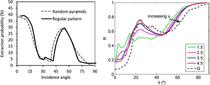
Figure 10. (left) Computation of transmission in air and reflection coefficient R of a roughened GaN surface in high-index material, n = 1.4 (right) along ray-tracing.130 (right) electromagnetic131 computations. Also shown is the convergence of wave optics calculations toward geometrical optics as a function of relative feature size u = a/λ. The full curves are wave calculations with increasing values of u = 1.5–4.5. They slowly converge toward the geometric limit (dashed line). From David.131
The simulations also demonstrate that the extraction efficiencies are only weakly or moderately sensitive to the variations of the extracting features (sizes, filling factors, etc.).130,131
Let us describe how surface roughening and PSS operate: the former relies on both ray randomization and increased single pass extraction (Fig. 11) while the latter only relies on ray randomization only.130 A drawback for surface roughening is that it is not well adapted to p-side up LEDs on sapphire substrates because it is difficult to etch the p materials, and it requires a current spreading layer on top of the p-GaN, usually ITO or a semi-transparent metal because of the poor p-GaN conductivity. The high performance surface roughened LEDs are therefore realized either using a p-side up LED on GaN substrate with back roughened n-type surface or in flip chip geometries using a substrate lift off.
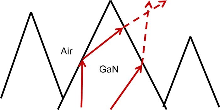
Figure 11. The change in direction of a totally internally reflected beam inside the pyramid of a surface roughened LED leads to approximately double the escape probability because there are typically two chances for an incident ray to escape the material.
Although based on somewhat different mechanisms, simulations show that both surface roughening and PSS lead to high ηLEE (Tables 9.2, 9.3, 9.4 in Lalau-Keraly130), using the same device parameters. The simulations in Ref. 130 yield lower ηLEE's than in industry, either due to conservative values of materials parameters (industry has lower absorption, in particular for ITO and metals) or less aggressive designs (larger lossy contact areas than in industry).
Compared to these disordered designs, photonic crystals also lead to remarkable LEEs,133 but their main advantage is emission directionality,134,135 which does not seem yet a large enough advantage to offset the demanding fabrication technology. The one case where PhCs are really at an advantage is their use as polarization-preserving light extractors: in the case of light emission into a preferred linear polarization, such as for m-plane LEDs, roughening would not preserve the polarization as light undergoes multiple random depolarizing light scatterings. Using 1D embedded PhCs, Matioli136 realized a 1.8x directional extraction enhancement with a high polarization degree of 88.7% at 465 nm for m-plane GaN LEDs.
Simulations of Electrical and Electro-Optical Properties
The development of simulation tools has two main drivers: they are needed to optimize device structures, in particular to optimize performance. In an ideal situation, they could also provide directions for new device architectures. Another use which was clear along the many preceding topics is their use for deciding which internal mechanisms are at play in LED operations, although one often relies then on circular arguments, the parameters used in the simulations having ad-hoc values to adjust simulations results to experiments.
1D simulations
There are several 1D LED simulations tools such as Silense,137 Tibercad,138 Comsol,139 Crosslight.140 However, these tools, when used with standard parameters such as energy band discontinuities and spontaneous polarization values and piezoelectric coefficients, fail in describing the blue LED forward voltage, yielding 3.4 V or more, while observed values are well below 3 V, quite smaller than the built-in junction voltage, about 3.2 V, and related to the photon energy by eVturn-on ≈ hν. To improve the simulation software results, the relative conduction band and valence band offsets (CBO and VBO, respectively) between GaN and InGaN are adjusted and the polarization charge at the heterointerfaces is also adjusted between 30 and 70% of the calculated value.141 There is no clear justification for this adjusted polarization value. A quantum correction to the drift-diffusion equations has been invoked but it is itself adjusted to fit results.142
With such essential ad-hoc adjustments made, relying on modeling results to support carrier escape or overshoot models of droop is questionable, with results being also very dependent on the structure being modeled, most often quite different from the real commercial, optimized structures.
3D simulations
The widely used commercially available 1D device simulation tools fail to account for alloy disorder of InGaN QWs and AlGaN barriers. It is however clear that due to the large differences in atom potentials in the InGaN system the effects of alloy disorder will be strong, and that relying on the usual virtual crystal approximation (VCA) used in common II-V alloys will be insufficient.143,144
For optical properties such as absorption or emission, i.e. when not including 3D transport modeling, random alloy effects can be calculated by solving Schrödinger equation for electrons and holes in the disordered potential due to compositional fluctuations. The potential is either computed from first principles145,146 or from the effective mass approximation (EMA).147–149 Such computations are already extremely demanding on computing resources, with the number of mesh nodes in finite elements computations exceeding a few ∼105 for typical blue LED structures.
Even taking disorder into account, there are still discrepancies between simulations and experiments. At high In contents beyond blue emission, one cannot retrieve the correct emission wavelength. For green LEDs, green emission is experimentally obtained with 24% of In while computations require more than 30% In to reach green wavelengths.150,151 A first explanation could be a large Stokes shift between computed bandgap and luminescence, increasing nonlinearly with In concentration.152,153 It is however difficult to identify the mechanisms leading to Stokes shifts as large as 300meV, maybe due to relaxation into deeply localized states, so far not identified. It rather seems that such large Stokes shift values are due to incorrect determination of the bandgap. Other explanations invoke large interface roughness or QW thickness fluctuations.154 The discrepancy could also be due to the use of a too small bowing parameter b (which describes the quadratic variation of bandgap with In concentration154) which would then underestimate the size of energy fluctuations (one usually takes b = 1.4 eV whereas some computations point to much larger values145). The accurate experimental determination of the bowing parameter is itself a challenge due to the differences obtained when choosing the PL emission wavelength, the absorption edge (an ill-defined quantity for disordered semiconductors) or reflectivity measurements as defining the bandgap. While clustering, observed by TEM, was early on disregarded as due to TEM measurement artifacts (observable clustering was created under strong electron irradiation), a recent paper suggests the existence of short range clustering, not to be seen in TEM and not detected in Atomic Probe Tomography (APT) analysis due to the limited detection efficiency of most APT systems.155
Calculations are limited to small volumes and to the first few quantum states, not allowing for simulations of transport properties in full devices due to the extreme demand on computing resources when calculating solutions of the Schrödinger equation. It was recently shown that a simplified model of disorder computations can account for many properties of nitride alloys such as the Urbach tail of absorption149 or the low turn-on voltage of blue LEDs.67 This novel theoretical and modeling tool of disorder is based on the Filoche-Mayboroda localization landscape theory,156 extracting from the original disordered energy map an effective potential, which allows use of standard transport equations while accounting for quantum effects due to the microscopic disorder.
For full heterostructure LED devices the 3D simulations must self-consistently account for the carrier-induced modifications of internal potentials and the changing 3D potential over a wide range of diode biases. A Schrödinger-Poisson drift-diffusion solver should be used to calculate energy levels, density of states, and transport properties under such circumstances. Compared to computations of optical properties, an electro-optical computation of LED operation requires typically 45 different voltage values and 16 iterations on average to achieve self-consistency. One uses the 3D Drift-Diffusion Charge Control (3D-DDCC) solver157 to simulate the electrical behavior of semiconductor devices by self-consistently solving the Poisson, landscape, and drift-diffusion equations in 3D structures. In the 3D-DDCC solver, the Schrödinger equation is replaced by the landscape equation:
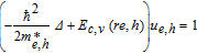
where m*e, h is the effective mass of the electron/hole, Ec, v is the conduction/valence band energy, and ue, h is the landscape function for the electron or hole, respectively.148 The landscape equation is used to predict the energy levels and local density of states (LDOS) in place of the Schrödinger equation. Its solution is much faster as it is a linear differential equation instead of an eigenvalue differential equation. The quantity 1/u is interpreted as the effective potential for the carriers, accounting for their quantum nature and particular behavior, such as confinement in a quantum well or tunneling through a barrier.67 The use of the landscape equation in lieu of Schrödinger's equation leads to a gain of 103 in computing speed, making 3D self-consistent computations possible (Table III). The complete description of the method and parameters used can be found in Reference 67. All simulations presented use 100% of the known values for the spontaneous and piezoelectric polarization parameters.141 It enables the description of transport in full blue LEDs, forward voltage and emission wavelength, without adjustment of parameters, only considering random alloy fluctuations.57,101 The lowering of bias voltage is due to carriers being transported preferentially through regions of lower effective bandgap, leading to percolative-type carrier transport. The same simulation displays a strong enhancement of droop due to Auger recombination because of the enhanced carrier concentrations due to carrier localization in lower energy regions.62
Table III. (left) Comparisons of computational times of energy levels by solving Landscape67 or Schrödinger equations147,150,159,160 in disordered nitride structures; (right) full LED electro-optical simulation times for classical (3D Poisson, 3D drift diffusion) single iteration (top) or (bottom) self-consistent 3D Poisson-DD-classical67), 3D Poisson-DD- Schrödinger or 3D Poisson-DD- Landscape in disordered nitride alloys and LEDs (After Li67).
| Node number | Computation | LED-One Iteration | Node number | Computation | |
| One Iteration | (matrix size) | time (s) | no disorder | (matrix size) | time (s) |
| 3D Localization landscape (e & h) | 428,655 | 50 | 3D Poisson | 428,655 | 25 |
| Schröd. Eq. Li | 428,655 | 63,650 | 3D Drift-diffusion (e & h) | 428,655 | 50 |
| Schröd. Eq. Watson-Parris | 1,500,000 | 60,000 | |||
| Schröd. Eq. Schulz | 328,000 | 7,500 | "Self-consistent" solver for | "Estimated" Total | |
| Schröd. Eq. Auf DerMaur | 100,000 | 24,000 | 45 bias point of LED | computation time (s) | |
| 3D Poisson-DD classical disorder | 54,000 | ||||
| 3D Poisson-DD-Schrödinger | 45,882,000 (531 days!!) | ||||
| 3D Poisson-DD-1/u | 90,000 (∼1 day) |
A few results of such computations are shown in Figs. 12 and 13. The experimental J-V curve is well reproduced with known polarization parameters. The electrons and holes are unevenly distributed among QWs (Fig. 12b). One recovers the hole transport mostly limited to the p side of MQW LEDs structures. The electron current through the LED structure undergoes complex trajectories, similar to percolation paths in disordered systems, as carriers transport in the perpendicular directions to QW planes through regions with lower energy barriers (Fig. 13).62,67
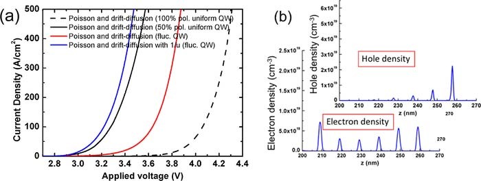
Figure 12. (a) I-V computations; dashed curve: classical Poisson-DD equations assuming full polarization in the LED structure; red curve: Poisson-DD equations with classical treatment of disorder; black curve: no disorder, classical Poisson-DD equations assuming 50% polarization; blue curve: Landscape theory treatment of disorder with classical Poisson-DD equations; (b): Carrier distributions in a 6 well MQW blue LED, J = 20 A/cm2 (from Li67).
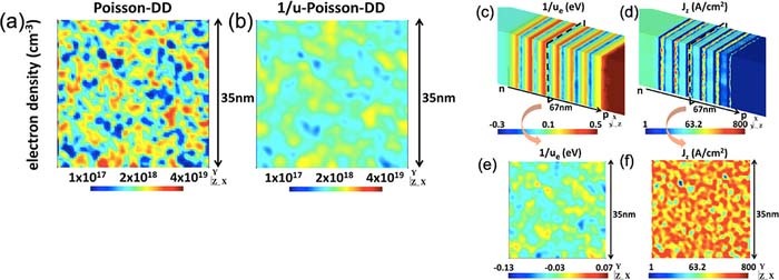
Figure 13. (a), (b) Computed self-consistent in-plane electron density in the midplane of the third QW of a 6 QW LED with compositional disorder at 20 A cm−2 current density using: (a) the classical Poisson and drift-diffusion models; (b) the landscape theory implemented in Poisson-DD. The true carrier density map is smoother as the quantum effects of confinement and tunneling diminish the amplitude of the effective potential fluctuations; (c,d) Perspective views of the localization landscape (1/u) and the normal component of current (Jz) calculated for a multiple quantum well LED. (e), (f) 1/u and Jz value maps in the midplane (x-y plane) of the third QW, LED current density is 20 Acm−2 (from Li67).
For the sake of completeness, it must however be mentioned that even this 3D model including disorder does not describe well green LED results for two important parameters: the computed turn-on voltage is too high by about 0.5 V, and the wavelength for a typical experimental In concentration of 24% is too short by about 30 nm compared to experiment. Tentative reasons for such disagreements could be incomplete description of the real commercial structures with advanced doping or compositional schemes, or oversimplified theoretical analysis. This is clearly an ongoing challenge, as it is a prerequisite for the rational design of long wavelength LEDs.
The localization of carriers by alloy fluctuations has been directly observed recently by scanning tunneling luminescence (STL).161
The Future: Reaching the Limits, and More ...
Possible solutions for current droop
The assignment of droop to an intrinsic mechanism indicates that remedies must address the mechanism itself, by reducing the carrier density for a given current density, i.e. that it is not solved by better quality materials or simple changes in designs, as would be for instance required if droop were due to defects87 or to carrier overshoot.64 The clear path to diminish the impact of Auger NR recombination is to diminish the carrier density by using larger active regions. This is the most widely attempted technique so far. An obvious solution, coming at a cost, is to incorporate in LED lamps many LED chips as a given total current will be spread over a larger area.
The volume carrier density can also be reduced by using thicker active layers. Gardner et al. demonstrated early that the use of a thick double heterostructure active layer could lead to a higher current density for the onset of droop.162 However, this solution does not seem to be implemented industrially, most certainly because the peak IQE is lower than for thin multi QW active layers because of poorer materials quality. Another way to increase the active volume thickness is by increasing the number of QWs. There is however a limit to uniform carrier injection and it seems that this is reached by industry for 5 to 9 QWs. A recent elegant proposal to increase the number of QWs while still retaining efficient carriers throughout the LED is to stack LED structures connected together via tunneling junctions.163 Multijunction LEDs have been demonstrated.164
Solving the green gap, and beyond
A first component of the poor WPE of green LEDs is the excess supply voltage compared to the photon energy. It is due to the poor inter-well transport in vertical stacks in MQW LEDs.165 A nice solution could be the use of lateral V-pits as demonstrated in Jiang82 (see the impact in Fig. 5). However, in such structures, the issue of droop is still not solved, most certainly due to the short lateral diffusion length of holes which leads to inhomogeneous carrier distributions, locally enhancing Auger NR recombination. Droop in green LEDs, similarly to blue ones, will require designs that lead to uniform carrier populations in the whole active volume. The IQE should also be improved by better growth, and the discovery of novel recombination mechanisms95,102 should help direct growth efforts.
Realization of > 100% WPE LEDs!
Physical limits of LED efficiency: a brief historical note
This question started with concerns about the efficiency limit of fluorescence and phosphorescence studies in the 1920s. It seemed at the time that anti-Stokes emission (emission at a shorter wavelength than the absorbed light) violated the second law of thermodynamics if sustained continuously (the first law, energy conservation, could be satisfied by the emitting material drawing energy from the environment). A controversy erupted with Lenard,166 Pringsheim,167,168 Vavilov169,170 being the main actors. The discussion evolved around the question whether the transformation of incoming light into anti-Stokes light could be a reversible or irreversible process, as if reversible (the claim of Vavilov169,170), it would contradict the second law. Vavilov identified light to work in the sense of thermodynamics, neglecting its entropy. The matter was settled by Landau171 in a remarkable analysis of the thermodynamics of luminescence where he considered the light entropy, and showed that the light entropy was increased from the directional exciting light to the spontaneously emitted light in all directions, thus obeying second law (for a more complete discussion of the controversy, see Mungan172). Therefore, surprisingly, one can have an efficiency of fluorescence above 100% by transforming some heat into photons, the luminescence of materials playing the role of a heat engine, like the compressor in a refrigerator.173
The path to 100%+ LEDs
The same question of physical limits exists, of course, for LEDs with their direct conversion of electricity into light. We saw in 2.1 that the WPE is equal to ηEQE x hν/qVbias. Normally, one expects the maximum WPE as a function of bias to be somewhat below unity, as both ηEQE and hν/qVbias are usually below unity. This is obvious for ηEQE. hν/qVbias, should also be <1 as one expects energy losses of injected e-h pairs to the lattice. However, through the carrier-lattice interaction, the LED carriers could gain energy from their environment, leading to hν > qVbias. One could then expect power efficiency larger than unity for emitted photons if injected electron hole pairs get an energy boost from the lattice thermal energy. As mentioned above, already in 1953, Lehovec33 remarked that emitted photons could have an energy larger than that of the energy of electrically injected electron hole pairs, eVbias. The energy gain was attributed to the energy drawn from the lattice thermal energy (Fig. 14).
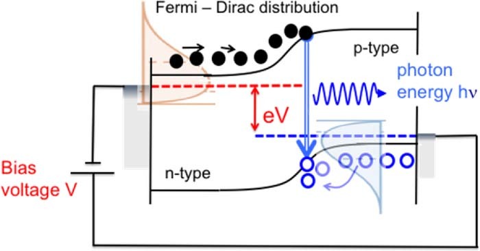
Figure 14. Illustration of light emission at the bandgap energy for an LED electrically injected at an electron-hole pair energy lower than the bandgap. Electrons and holes are "boosted" to energies higher than their injected energies thanks to the high-energy thermal tail of e-h distributions created by the thermal phonons of the lattice at finite temperature.
In 1956 Bradley applied already for a quite complete patent on a cooling device from a high efficiency light emitting p-n junction.174 He discussed applying the concept to Ge and Si, and ways to improve their efficiency, but he also mentioned that direct gap semiconductors might have higher recombination efficiency, hence a better chance of absorbing more heat from the lattice than releasing heat through NR recombination, thus indeed cooling the lattice. The issue of reabsorption for bulk materials was to be solved by placing the emitting volume near the surface of the device. More experimental data came in 1962 when Keyes and Quist175 remarked that injection of carriers near the band edges in GaAs could result in cooling. The first evidence that the average photon energy could be larger than the supplied energy came in 1964176 in a forward biased GaAs diode. However, the IQE was too small to prevent overall heating of the diode. The fact that the LED can overall act as a refrigerator conversely meant that the overall electrical energy efficiency (WPE) could be higher than unity by drawing thermal energy from the surroundings.
It should be noted that, due to the need to have alternatives to the existing cooling techniques in microelectronics (thermo-electrics, cryo-generators, cryo-fluids), the search for photoluminescence or electroluminescence cooling has attracted much more efforts than increasing LED WPE by thermoelectric carrier pumping.177
The tackling of cooling by light emission has thus drawn huge efforts, the most well-known being that of laser cooling of atoms. A pioneering analysis was given by Kastler178 in the context of optical pumping which could be used to cool down the internal degrees of freedom of optically pumped atoms and further cool down by collisions atoms of a buffer gas, an effect which he calls "lumino frigorifique". He extended his concept so far applied to magnetic sublevels of atomic vapors to the Stokes and anti-Stokes lines due to crystal fields in rare earth ions in crystalline matrix, reviving the concepts of Pringsheim.167,168 As we know, optical pumping quickly developed into a major tool for the study of atomic spectroscopy, for which Kastler received the Nobel prize in 1966. The other major cooling method in atomic physics, for which Chu, Cohen-Tannoudji and Phillips received the Nobel prize in 1997, was the use of detuned laser excitation for atomic vapors leading to the progressive slowing down of the translational motion.
In solids, net radiative cooling was much more difficult to observe because of the parasitic effect of non-radiative recombination. The first demonstration of cooling of a solid was performed in 1995 on Yb+3 doped heavy metal fluoride glass179 where the losses associated with electrical carrier injection are avoided through laser optical excitation.
As for semiconductor LEDs, it is interesting to note that while lattice cooling was invoked as early as 1953,33 the first demonstration of overall LED cooling was very recently done indirectly by observing an LED power efficiency larger than unity in infrared LEDs, which by difference implies that energy has been taken from the surroundings.180 This relies on the inspection of the equation for WPE, WPE = ηEQE x hν/qVbias, which can be made arbitrarily large by diminishing Vbias. The price to pay is a vastly diminishing current density, varying roughly exponentially according to Shockley diode equation. Also, the IQE diminishes as
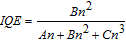
It would then seem that the radiative efficiency would diminish to zero with voltage as the carrier density would vanish, but at extremely low bias such that Vbias < kT/q, the active region excess carrier concentrations become negligible compared to the equilibrium carrier concentrations n0 and p0, and the IQE
becomes independent of voltage. Then, considering the ηIE, ηEE, and ηLEE as independent of voltage, the WPE will vary as 1/Vbias and can reach values above unity. This is seen in Fig. 15 for the case of mid-IR LEDs.180
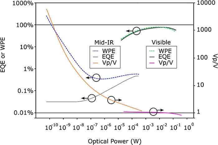
Figure 15. Relationship for EQE, WPE, and electrical efficiency Vphot/V on emitted optical power for the mid-IR LED reported in Ref. 180 and for the nitride blue LED reported in Ref. 132. The IR LED WPE curve has two peaks, the conventional peak near the EQE peak, and the other at low bias where the EQE saturates as Vphot/V continues to rise with diminishing V. The WPE exceeds 100% at an EQE of 0.03% and Vphot/V of ∼700%. (figure reprinted from Ref. 122).
From this discussion, it would seem that WPE larger than 100% can only be reached at vanishingly small, useless currents. There is however another operating point with qV < hν, for which WPE might be larger than unity provided the ηEQE is large enough, at useful current densities (Fig. 15).122,132,181–183 This would occur at voltages near but less than Vphot = hν/q, such that a sizeable thermal energy pumping from the lattice hν-qVbias per e-h pair is obtained, but not too far from hν/q so that the EQE is large enough to have WPE = ηEQE x Vphot/Vbias >1 although operating the LED below its peak EQE. A first attempt was done on nitride LEDs by Xue et al.181 More recent nitride measurements132 are shown in Fig. 15. A discussion on how to reach 100% WPE nitride LEDs is given in Ref. 122.
Conclusions
The field of nitride LEDs has seen remarkable progress in both performance and understanding. There are however still a number of open questions, and room for improvement, would it only be for a simulation tool which would describe LED operational features at all wavelengths. Central is the correct description of alloy compositional fluctuations. It is also remarkable that new recombination mechanisms and measurement techniques are being discovered which will allow optimization of LEDs for all demands. Finally, the search for 100% WPE LEDs opens an intriguing challenge.
Acknowledgments
This work has been partially supported by grants No. 601954 and 601952 from the Simons Foundation, by the NSF RAISE-TAQS grant DMS 1839077, and by the U.S. Department of Energy under award No. DE-EE0007096. The author acknowledges a long collaboration and many useful discussions with Prof. J. Speck, And Dr. A. David for discussions about many items in this paper.
ORCID
Claude Weisbuch 0000-0001-5403-5274