Abstract
The electrochemical engineering aspects of high aspect ratio cells, such as those used in in situ electrochemical scanning transmission microscopy (ec-S/TEM) were examined, focusing on aspects that could cause non-uniform current distribution. Having a uniform current distribution across the working electrode is important for any spectroelectrochemical technique in order to provide accurate electrochemical information as well as structural electrolyte-electrode interface information. An analytical model was developed to determine current density distribution and a Wagner number was derived for a small cell height with coplanar electrodes. The main assumptions of this analysis are: 1) mass transport effects are negligible, 2) a uniform potential distribution in the direction of the cell height due to their small size, and 3) the working electrode potential is constant across its length. With our analysis, the assumptions were found to be reasonable. In addition, the effect of the conductivity and thickness of the thin film electrode and its potential effect on current density distribution have been analyzed. Now, with this work, high aspect ratio cells with a small cell heights and coplanar thin electrodes can be analyzed to determine their current density distribution.
Export citation and abstract BibTeX RIS

This is an open access article distributed under the terms of the Creative Commons Attribution 4.0 License (CC BY, http://creativecommons.org/licenses/by/4.0/), which permits unrestricted reuse of the work in any medium, provided the original work is properly cited.
In situ surface probing of the electrode-electrolyte interface is of interest when characterizing surface intermediates and phenomena such as electronucleation and electrodeposition. Some of these methods have the ability to elucidate electrode-electrolyte interfaces of interest and they bypass problems inherent to ex situ analysis such as surface restructuring and ex situ surface reactions. Existing in situ methods include: in situ atomic force microscopy (AFM),1 in situ spectroelectrochemistry2 (such as Raman spectroscopy3,4 and UV/Vis5), in situ electrochemical scanning tunneling microscopy,6 and the more recently developed in situ electrochemical scanning/transmission electron microscopy (in situ ec-S/TEM).7–23 In situ ec-S/TEM has the unique capability of a performing quantitative electrochemical measurements while simultaneously acquiring real time, high spatial resolution images. In situ ec-S/TEM has been used for observing time-resolved electrochemical nucleation in nanometer resolution,7,8,12,13 dendrite formation,16,17 solid-electrolyte interface formation and life cycle,14,18,19,21,22 and has been shown to yield verifiable diffusion coefficients.8,20 These techniques can be used to develop electronucleation models which give insight with regards to the nucleation density, nucleation rate, and nucleation mechanism.24–30 Controlling electronucleation is critical to developing electronics, batteries, protective coatings, and other application that utilize thin film technologies. In contrast, ex situ analysis encounters various issues include surface restructuring and the inability to verify nucleation density and initial spatial distribution of nucleation sites.
In situ ec-S/TEM is a relatively new characterization technique that utilizes MEMS fabricated microchip devices. The working, reference, and counter electrodes are coplanar and have been micro-fabricated on a single microchip otherwise known as the electrochemical chip. The working electrode is fabricated over SixNy which acts as an electron transparent medium and a barrier to the TEM vacuum. A spacer chip is placed facing the electrochemical chip with the liquid electrolyte sandwiched between the spacer and electrochemical chip. The spacer chip dictates the height of the cell and thus the electrolyte layer thickness. An assembly view of a commercially available in situ ec-S/TEM system (Protochips, Inc. Morrisville, NC) is shown in Figure 1.
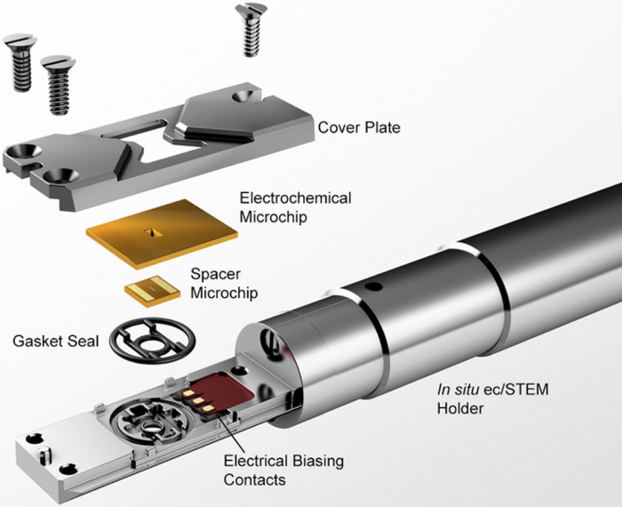
Figure 1. Illustration of the in situ ec-S/TEM holder. The electrochemical and spacer chips are sealed within the tip of the in situ ec-S/TEM holder and encapsulate electrolyte that is delivered by microfluidic tubing (not shown). The microfabricated electrochemical chip contains the working, reference, and counter electrodes that interfaces with a potentiostat via electrical biasing contacts and wires.
An in situ ec-S/TEM cell has a very thin cell height (on the order of 10 and 1000s of nanometers from the surface of the electrode to the window above it) compared to the length of the working electrode (10 μm) and distances from the working electrode to the reference and counter electrodes (on the order of 50 μm and 500 μm). This is due to the electron beam pathway needing to be small to mitigate scattering which is detrimental to image resolution.15 Due to the high aspect ratio (length of working electrode relative to distance from electrode to window above) this type of cell design is very likely to yield non-uniform current distribution as compared to conventional electrochemical cell designs. However, in order to correlate electrochemical overpotential with current density at the interface under observation (e.g. nucleation or morphology characteristics), it is desirable to have a uniform current distribution along the electrode. This way the applied potential can be corrected in a simple manner for ohmic drop, and the correlation of activation overpotential with current flux is known. If the current distribution is non-uniform, then it is much more difficult to correlate observed nucleation and morphology mechanisms with the measured current and overpotential, thus causing measurements and observations to be ambiguous. However, the current and potential distributions in these types of co-planar high aspect cells have not yet been rigorously examined.10,11,23,31–34
This work aims not only to understand the implications of in situ ec-S/TEM cell geometries on current density distribution but it is generally applicable to any spectroelectrochemical technique using similar cell designs. Once the effects of cell design and operating factors are better understood, then in situ imaging and electrochemical data can be correlated with confidence and mechanisms such as electronucleation can be studied more rigorously. A cuprous bromide electrolyte at high concentration is examined in the experimental studies because of recent interest in this chemistry due to its potential use in flow batteries.35,36
Experimental
Electrochemical chip processing
A Protochips electrochemical chip with a carbon working electrode, silver reference electrode, and platinum counter electrode were used in conjunction with a windowless 500 nm high spacer chip. The electrochemical chip was cleaned by first soaking in acetone to remove the protective photoresist then rinsed with methanol. The spacer chip was cleaned with methanol. Both chips were then argon plasma cleaned for approximately 30 seconds to make the Si3N4 window hydrophilic.
After plasma cleaning, the chips were then assembled into the Protochips Poseidon 210 cell. An electrolyte of 4M NaBr/0.1M HBr was then pumped through the cell at approximately 5 to 10 μL min−1 until the cell completely wetted. The reference electrode was then converted by anodic polarization from a silver pseudo reference electrode to a silver-silver bromide reference electrode. A 50 nA oxidative current was set to a square wave cycle of 0.5 seconds on and 0.5 seconds off for 3000 cycles. (Note that since a high bromide electrolyte was used, a silver-silver bromide reference electrode was necessary. It is important to note that, in a chip-type cell like this, the reference electrode is exposed to the same electrolyte as the working and counter electrodes, and therefore has to be compatible with the electrolyte for a stable reference electrode. After the reference electrode was processed, the electrolyte containing 4M NaBr/0.1M HBr/0.1M CuBr was then pumped through the cell.
In situ electrochemical optical microscopy experiments
A Biologic SP-200 potentiostat was used to conduct electrochemical measurements. A Mitutoyo optical microscope was used in conjunction with Camtasia software to visualize and record electrochemical growth, and a Harvard Apparatus Pico Plus syringe pump was used to pump electrolyte.
An electrolyte of 4M NaBr/0.1M HBr/0.1M CuBr was pumped at 1 μL min−1. A potentiometry scan was then conducted, to estimate the standard potential of the reaction, from -0.5 to -0.85 volts at a scan rate of 1 mV s−1. The experiment was stopped after approximately 10 nA of reductive current was observed. The approximate standard potential was estimated to be the potential when 5 nA of reductive current was achieved. This was the potential at which the current would consistently stay reductive. A chronopotentiometry experiment was conducted at 20 nA of oxidative current for 3 minutes or 0.36 μC to oxidize the copper electrodeposited during the potentiometry experiment. Then, the chronoamperometry experiment was conducted at the desired overpotential until 0.306 μC of reductive charge was passed. This amount of electrodeposition allowed easy visualization of the growth in the optical microscope. A second chronopotentiometry experiment was then conducted with the same parameters as the previous chronopotentiometry experiment to remove the electrodeposited copper. This process was repeated for each desired overpotential.
Results and Discussion
The approach to cell analysis taken here is to assume adequate reactant availability for reaction assume negligent reactant concentration effects, and to solve the primary/secondary current distribution problem. To test these assumptions, the concentration of a one electron reactant needed to sustain a current density of 3000 A m−2 on a 2500 μm2 electrode in a typical commercial ec-S/TEM cell is estimated. In situ ec-S/TEM experiments can be conducted with flow rates of 1−20 μL min−1. Larger flow rates may be limited by SixNy window strength. The amount of current that can be sustained as a function of flow rate and concentration is estimated in Figure 2. A current density of 3000 A m−2 corresponds to a total current of 7.5 μA in this example. A flow rate of 3 μL min−1 of a 5 mM solution is equivalent to a current of 24 μA (approximately 9600 A m−1), which should be adequate for most studies. An example calculation for a one electron process 'n' with a concentration of 5 mM and a flow rate of 3 μL min−1 is shown in Equation 1. The unit conversions were neglected for ease of readability. Therefore, reactant stoichiometry limiting effects are negligible. Using the gap distance (height) between the working electrode and the window as a conservative estimate of the boundary layer thickness, then for a one-electron transfer reaction assuming a diffusion coefficient of 10−5 cm2 s−1 and an entering reactant concentration of 5 mM, the limiting current density is estimated to be 965 A m−2 for a 0.5 μm gap, and 9650 A m−2 for a 0.05 μm gap, respectively. These limiting currents could be higher by an order of magnitude for developing boundary layers due to electrolyte flow. Consequently, the assumption is reasonable that mass transfer effects are negligible as well because of the flowing electrolyte in a thin gap and suggest that tertiary current distribution effects can be ignored.
![Equation ([1])](https://content.cld.iop.org/journals/1945-7111/166/4/H126/revision1/d0001.gif)
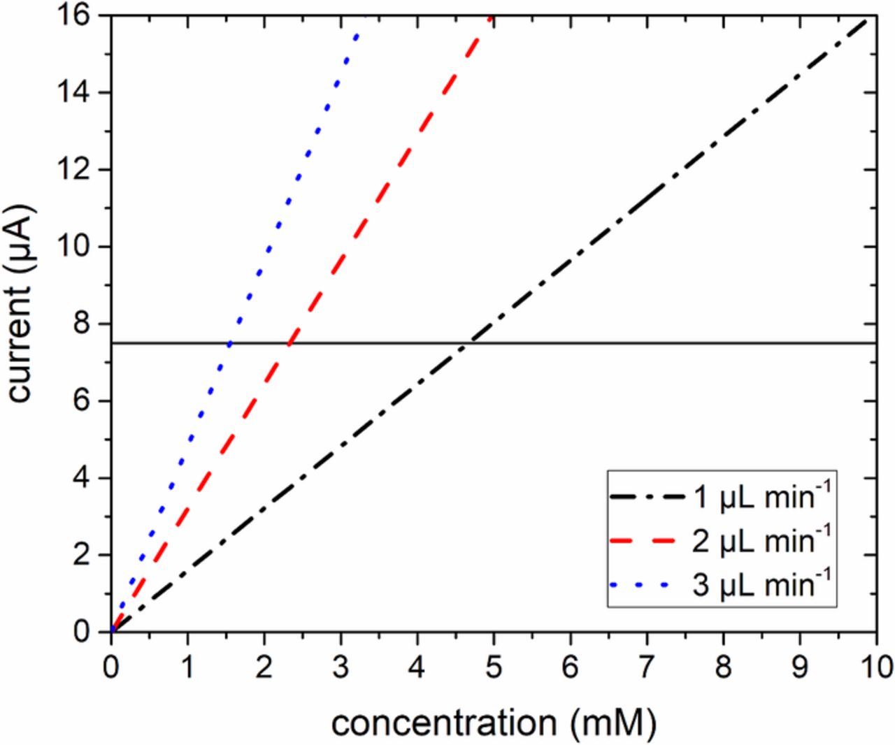
Figure 2. The amount of a 1 electron reaction reactant current capable of sustaining 3000 A m−2 on a 2500 μm2 working electrode as a function of concentration and flow rate: flow rate of 1μL min−1 (black dash dotted line), 2 μL min−1 (red dashed line), and 3 μL min−1 (blue dotted line). The black horizontal line corresponds to a current density of 3000 A m−2 on a 2500 μm2 working electrode.
Analytical current distribution analysis
The in situ ec-S/TEM cell consists of an electrochemical chip, the spacer chip that defines the cell height between the electrode surface and the window above it, with liquid electrolyte encapsulated between. A typical electrochemical chip is shown in Figure 3. Because the gap between the electrode surface and the parallel window above is so small, on the order of nanometers-to-microns, the normal placement of counter and reference electrodes must be on the same plane as the working electrode at distances much greater than the cell height (channel gap). The geometry in Figure 3 has been simplified for ease of analytical evaluation as shown in Figure 4. The simplified geometry is as follows: the working electrode is an ellipse with the a-axis = 12.5 μm and the b-axis = 50 μm giving a working electrode area of 1964 μm2. The reference electrode is formed by two ellipses: an inner ellipse with a-axis = 100 μm b-axis = 137.5 μm, and an outer ellipse with a-axis = 110 μm and b-axis = 147.5 μm. The counter electrode is comprised of two circles the inner circle radius is 500 μm and the outer circular radius is 600 μm. The origin is in the center of the working electrode. The cell height (h) is in the direction normal to the electrode, and the commercial cell has a silicon nitride window with h = 0.5 μm or with h = 0.05 μm.
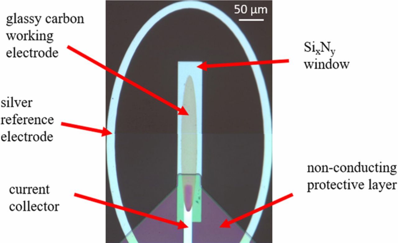
Figure 3. Light optical micrograph of a commercial electrochemical chip. The working electrode is glassy carbon, the reference electrode is silver, and a silicon nitride window allows electrons to pass through. The working electrode connection to the current collector and the entire current collector is covered in a non-conductive protective coating. The counter electrode is not shown in this image.
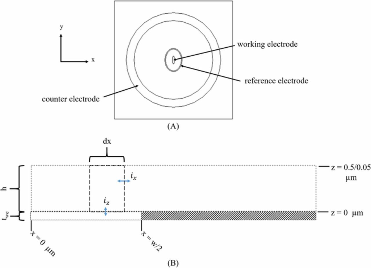
Figure 4. (A) A representation of the Protochips electrochemical chip. The working electrode is an ellipse with an area of 1964 μm2 and the center of the working electrode is the origin with (x, y, z) = (0,0,0). The reference electrode is an ellipse geometry and the counter electrode is a circular geometry. Typical dimensions are given in the text. (B) The geometry and current directionality of the analytical model. h is the height of the cell and the volume element, dx is the incrementally small portion of the width of the volume element in the x direction, iz is the current density in the z direction entering or leaving the volume element from the electrode, ix is the current in the x direction entering or leaving the volume element, and d is the width of the volume element in the y direction (normal to the page).
For this analysis, further simplification of geometry takes into account symmetry as shown in Figure 4. There are three main assumptions to this analysis:
- (1)There is no reactant stoichiometric or mass transport limitations as shown in the previous section.
- (2)The potential along the z axis is constant due to the small cell height size. The reasonableness of this assumption is examined by comparing to a rigorous numerical solution without this assumption.
- (3)The working electrode metal-phase potential is constant along its length. This will be discussed in detail below.
A current balance over the volume element as shown in Figure 4 can be written as
![Equation ([2])](https://content.cld.iop.org/journals/1945-7111/166/4/H126/revision1/d0002.gif)
where the symbols are defined above and in Figure 4.
At the limit of dx→ 0, the current balance simplifies to:
![Equation ([3])](https://content.cld.iop.org/journals/1945-7111/166/4/H126/revision1/d0003.gif)
Assuming linear kinetics:
![Equation ([4])](https://content.cld.iop.org/journals/1945-7111/166/4/H126/revision1/d0004.gif)
where io is the exchange current density, n is the number of electrons in the reaction, F is Faradays constant, R is the gas constant, T is the temperature, Φ1 is the potential in the electrode phase (assumed to be constant), and Φ2 is the potential in the electrolyte phase. When assuming the cell height is so small that an ohmic drop in the z axis is non-existent, Ohms law in the electrolyte simplifies to:
![Equation ([5])](https://content.cld.iop.org/journals/1945-7111/166/4/H126/revision1/d0005.gif)
where k is the conductivity of the electrolyte. Combining Equations 3–5 and arbitrarily setting Φ1 = 0, with dimensionless parameters defined below yields
![Equation ([6])](https://content.cld.iop.org/journals/1945-7111/166/4/H126/revision1/d0006.gif)
where the dimensionless potential and x-dimension are defined as:
![Equation ([7])](https://content.cld.iop.org/journals/1945-7111/166/4/H126/revision1/d0007.gif)
and
![Equation ([8])](https://content.cld.iop.org/journals/1945-7111/166/4/H126/revision1/d0008.gif)
In Equation 6, the dimensionless Wagner number, Wa, is defined as:
![Equation ([9])](https://content.cld.iop.org/journals/1945-7111/166/4/H126/revision1/d0009.gif)
where w is the width of the electrode (symmetry assumed in the center of the electrode). Note that in a classical secondary current distribution problem, the Wagner number comes from the boundary conditions only of the field equation, but in this analysis it comes into the current balance equation. Note that the characteristic length of this Wagner number is the ratio of the square of the electrode width to the height of the channel. As the characteristic length becomes larger, or the ratio of ohmic resistance (inverse to k) to kinetic resistance (inverse to io) increases, then the Wagner number decreases, and approaches a primary current distribution (the kinetic effects are negligible).
The boundary conditions for this geometry in dimensionless units are the following:
![Equation ([10])](https://content.cld.iop.org/journals/1945-7111/166/4/H126/revision1/d0010.gif)
![Equation ([11])](https://content.cld.iop.org/journals/1945-7111/166/4/H126/revision1/d0011.gif)
The first boundary condition above assumes symmetry along the center-line of the electrode (current in both directions to a surrounding counter electrode), and the second boundary condition assumes an arbitrarily chosen potential at the outer edge of the electrode that is constant along the z-direction. The solution of the above equation under these boundary conditions is given below:37
![Equation ([12])](https://content.cld.iop.org/journals/1945-7111/166/4/H126/revision1/d0012.gif)
The current distribution along the x axis is given by referring to Equation 4 with Φ1 = 0:
![Equation ([13])](https://content.cld.iop.org/journals/1945-7111/166/4/H126/revision1/d0013.gif)
To obtain the dimensionless current distribution, the current can be integrated along the electrode from x' = 0 to x' = 1 (Equation 9) to obtain the average current in the z direction (iz, avg):
![Equation ([14])](https://content.cld.iop.org/journals/1945-7111/166/4/H126/revision1/d0014.gif)
And the ratio of the local current at the electrode surface to the average current becomes:
![Equation ([15])](https://content.cld.iop.org/journals/1945-7111/166/4/H126/revision1/d0015.gif)
This dimensionless current density distribution as a function of the Wagner number is shown in Figure 5. As one might expect, as the Wagner number increases then the current distribution becomes more uniform. It was found that a Wagner number greater than 5 yields an essentially uniform current density distribution.
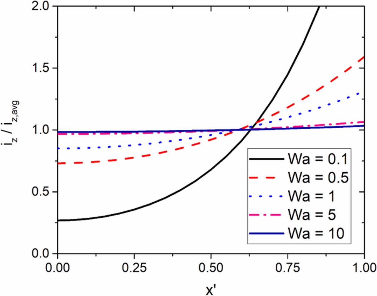
Figure 5. Normalized current density distribution of the analytical model shown in Figure 3 as a function of the derived Wagner number. A Wagner number greater than 5 yields a uniform current density distribution.
The cell parameters in the Wagner number are bounded by practical S/TEM image limitations. The cell height is limited to 1 μm due to loss of image resolution as a result of electron beam scattering.15 Assuming a temperature of 298 K and a 1 electron process, the maximum exchange current densities that yield a uniform current distribution are estimated as shown in Table I for cases satisfying a criterial of: a minimum Wagner number equal to 5, several practical values of cell height, typical values of conductivity (high to low salt/acid concentrations), and typical electrode widths. As shown, higher conductivities allow for faster electrochemical reactions (as noted by the exchange current density). However, increasing w2/h, by increasing the width or decreasing the height, decreases the allowable rate of an electrochemical reaction that can be studied.
Table I. Maximum exchange current density for an electrochemical reaction that will yield a uniform current distribution for various cell dimensions and conductivities in an ec-S/TEM cell.
| w2/h (μm) | k (S m−1) | io,max (A m−2) |
|---|---|---|
| 1250 | 34 | 560 |
| 1250 | 3.9 | 64 |
| 1250 | 0.41 | 6.7 |
| 12500 | 34 | 56 |
| 12500 | 3.9 | 6.4 |
| 12500 | 0.41 | 0.67 |
| 20000 | 34 | 35 |
| 20000 | 3.9 | 4.0 |
| 20000 | 0.41 | 0.42 |
| 200000 | 34 | 3.5 |
| 200000 | 3.9 | 0.40 |
| 200000 | 0.41 | 0.042 |
Examining the second assumption of the analytical model using a numerical method
Assumption two of the analytical model is examined here. This was done by relaxing assumption two, and numerically solving the field equation with appropriate boundary conditions for the two-dimensional case. The full model for the numerical approach, assumptions, boundary conditions, and method of solution are given in the appendix. Figure 6 is shows the potential distribution in the channel above the electrode for the case of the primary distribution, i.e. where kinetic resistances are negligible. As shown in Figure 6, the electrolyte potential is uniform across the cell gap, except near the edge of the electrode where there is some z-direction dependency.
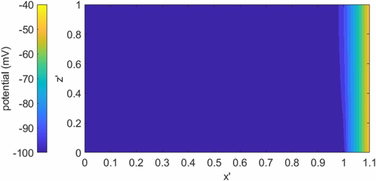
Figure 6. Potential profile in the primary current distribution numerical model for a conductivity of 4 S m−1 and a working electrode potential of 100 mV. Where x' = 1 is the edge of the working electrode and h' = 1 is the top of the cell and h' = 0 is the working electrode plane.
Table II shows the comparison of the secondary numerical current distribution model and the analytical current distribution model for a Wagner number of 0.1 at various positions along the x-axis. The highest normalized current difference is 0.021 which is a 2.4% difference indicating the analytical model is a good representation of the actual distribution of current and potential in the ec-S/TEM cell.
Table II. Comparison between the numerical and analytical model of normalized current density along normalized x axis.
| Wa = 0.1 | |||
|---|---|---|---|
| iz/iz,avg | |||
| x' | numerical model | analytical model | % difference |
| 0.2 | 0.327 | 0.324 | 0.92 % |
| 0.4 | 0.517 | 0.513 | 0.77% |
| 0.6 | 0.893 | 0.914 | -2.4% |
| 0.8 | 1.702 | 1.694 | 0.47% |
| 1 | 3.153 | 3.174 | -0.67% |
Examining the third assumption of the analytical model
The third assumption in the model above is that the working electrode potential is uniform across its width. However, a potential drop may occur in thin electrodes, as found in in situ ec-S/TEM configurations, due to electrode ohmic effects. An estimate of the potential drop in the working electrode is given by Equation 16 where ΔΦwe is the maximum potential drop along the working electrode in the y-direction in Figure 4 iz, avg is the average current density normal to electrode-electrolyte interface and is assumed to be uniform, σwe is the conductivity of the electrode material, Dwe is the distance along the working electrode away from the current collector, and twe is the thickness of the working electrode. If there is a high ohmic drop in the working electrode, then there will likely be a non-uniform current due to the electrode ohmic effects and consequently electrodeposition will likely occur closer to the current collector.
![Equation ([16])](https://content.cld.iop.org/journals/1945-7111/166/4/H126/revision1/d0016.gif)
Several conductivities for common working electrode materials are shown in Table III. The length (Lwe) of the working electrode is set by the design of the chip and is often approximately 100 μm. The average current density (iz, avg) depends on the applied overpotential and exchange current density. The maximum working electrode thicknesses is often limited to be less than 100 nm in order to prevent electron beam scattering. Potential drops in the working electrode were calculated for an average current density of 300 A m−2, which is well within the stoichiometric and mass transport limitations calculated previously, for several material conductivities as a function of working electrode thickness. The results are shown in Figure 7. A conductivity of 2 × 10⁴ S m−1 and an electrode thickness of approximately 40 nm with a maximum current density of 300 A m−2 and a distance of 200 μm (the likely total length of the electrode) represents a likely worst-case scenario where electrode ohmic effects might be an issue. As shown in Figure 7, in general electrode ohmic losses with electrode thicknesses greater than 40 μm are small and not likely to be a significant factor in these geometries.
Table III. Conductivities of various working electrode materials at 25°C.
| Working Electrode Material | σ (S m−1) |
|---|---|
| Glassy Carbon38 | 2 × 10⁴ |
| Platinum39 | 9.35 × 10⁶ |
| Gold39 | 4.43 × 10⁷ |
| Silver39 | 6.18 × 10⁷ |
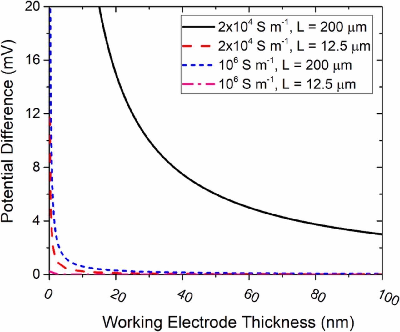
Figure 7. Potential drop along a working electrode at conductivities representative of typical electrode materials and for an electrode length of 200 μm and a current density of 300 A m−2.
Electrochemical measurements and results with an in situ ec-S/TEM cell
Electrochemical measurements in a one electron reaction process of cuprous bromide reduction were investigated using the in situ ec-S/TEM cell and imaged with optical microscopy in order to avoid any deleterious effects of electron beam induced radiolysis.40–43 These cells exist to check chemical stability and ascertain electron beam effects and these experiments can confirm the cell modeling results reported above. Optical images of the electrodeposits after plating are shown in Figure 8 with their respective approximate overpotentials. The lighter particle-like spots on the electrode are copper deposits growing from nucleation sites. Chronoamperometry scans for each overpotential can be found in Figure A2 located in the appendix. These experiments, per Table I, are within the w2/h and conductivity regimes of 1250 μm and 3.9 S m−1, respectfully. This indicates that uniform current density distribution will be observed along the width if the exchange current density is less than 64 A m−2. The exchange current density for copper electrodeposition is around this magnitude, and thus uniform current density distribution should be observed and, as seen in Figure 8, this is the case.
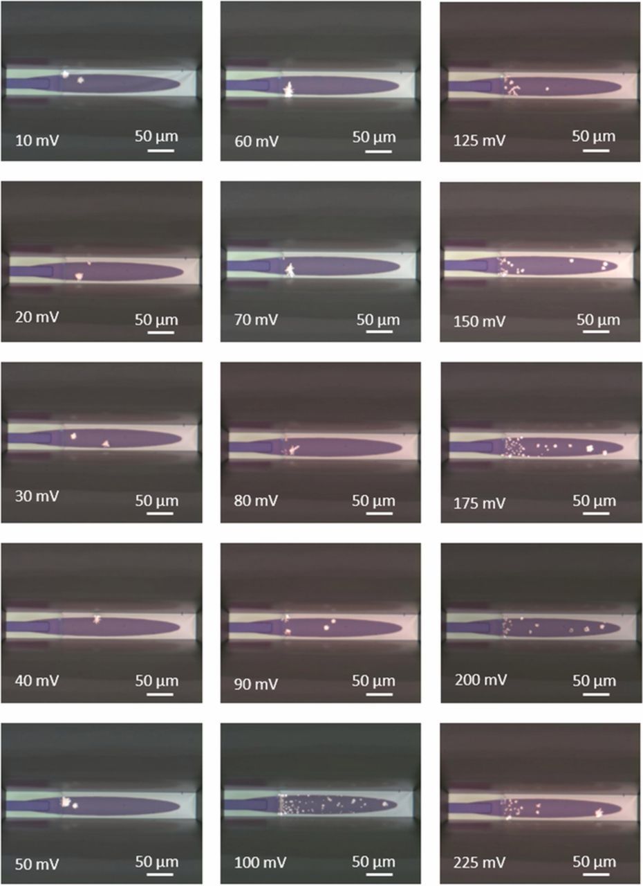
Figure 8. Light optical images following chronoamperometry experiments after plating 0.36 μC. Higher overpotentials tended to yield smaller but more numerous copper deposition growth areas than the lower overpotentials which yielded larger and less numerous copper deposition growth areas. In addition, it appears that copper deposition growth is favored near the current collector - near the left edge of each image. Overpotentials shown are approximate total overpotentials.

Figure A2. In situ electrochemical data of chronoamperometry of 10–50 mV (A) 60–100 mV (B) and 125–225 mV (C).
There are two major observations from these data sets worth noting.
- (1)Low overpotentials yielded less numerous and larger copper deposition growth areas whereas higher overpotentials yielded more numerous but smaller optically discernable copper deposition growth areas.
- (2)There is a higher propensity for copper to electrodeposit near the current collector than at the far end of the working electrode opposite the current collector in the in situ ec-S/TEM configuration.
Some explanations for these observations are examined here:
- 1) Low overpotentials versus higher overpotentials observation.
This result is to be expected. According to classical theory, low overpotentials have been seen in literature to have a lower number density of sites than higher overpotentials.44 However, there were some experimental anomalies; there were more deposits at the 100 mV overpotential observed than the 125 mV and 150 mV. The potentials for each chronoamperometry experiment were randomly selected. The 100 mV experiment was conducted chronologically after the 125 mV and 150 mV experiments which may indicate that the electrode surface morphology may be changing throughout the course of the experiments and creating more sites favorable for nucleation.
- 2) Electrochemical deposits near the current collector.
As indicated previously, electrode ohmic potentials drops of an electrode of a conductivity of 2 × 10⁴ S m−1 along a distance of 100 μm should be negligible. However, the electrode ohmic effect calculated previously assumes a homogenous electrode. Non-uniform electrodeposition might be related to non-uniformity of the fabricated electrode thickness or non-uniform distribution of active nucleation sites on the surface due to impurities. Surface impurities or fabrication processes that do not yield uniform surface coverage could lead to conductivities or resistivities that are a function of length and morphology45 of the surface that are not the bulk phase conductivities used to make the calculations above. The conductivities needed to explain the observed preferential electrodeposition near the current collector have been estimated. For this estimate, we assume that the potential difference due to electrode ohmic effects must be greater than the ohmic and kinetic overpotentials. With a Wagner number greater than 5, the kinetic overpotential dominates over the potential drop in the electrolyte. Therefore, the potential drop due to the resistance of the thin electrode only needs to be compared to the kinetic overpotential.
Rearranging Equation 4 to obtain activation or kinetic overpotential (ηa):
![Equation ([17])](https://content.cld.iop.org/journals/1945-7111/166/4/H126/revision1/d0017.gif)
The activation overpotential can now be calculated. iz is 300 A m−2 which is the current density used in the ohmic effects as a function of electrode thickness, n is 1, T is 298 K, and io of 30 A m−2 and 3000 A m−2 are used to show a range of kinetic overpotentials. The activation overpotentials are 0.26 mV and 26 mV for 30 A m−2 and 3000 A m−2, respectively. Therefore, the conductivities of 40 nm thick working electrodes must be less than 57,700 S m−1 and 577 S m−1, respectively, to see the preferential deposition near the working electrode.
Conclusions
An analytical model was developed to determine the current density distribution and the Wagner number for high aspect ratio cells with small cell heights that have coplanar electrodes. A uniform current distribution was found when the Wagner number was greater than 5. The three main assumptions of the analytical model were explored and found to be reasonable. Experimental results indicated that an effect other than kinetic and electrolyte ohmic effects was present due to the higher propensity to electrodeposit near the current collector. Electrode conductivities of 104 S m−1 for electrodes having a thickness on the order of 40nm should allow for a uniform current density distribution. However, experimental results indicate the actual thin film conductivities may be lower than known bulk conductivities and should be determined prior to experimentation.
Acknowledgments
This material is based upon work supported by the U.S. Department of Energy, Office of Science, Office of Workforce Development for Teachers and Scientists, Office of Science Graduate Student Research (SCGSR) program. The SCGSR program is administered by the Oak Ridge Institute for Science and Education (ORISE) for the DOE. The in situ ec-STEM work was conducted at Oak Ridge National Laboratory's Center for Nanophase Materials Sciences (CNMS), a U.S. Department of Energy Office of Science User Facility. ORISE is managed by the ORAU under contract number DE-SC0014664. Additional graduate support was covered by the Great Lakes Energy Institute Think Energy Fellowship and Walter J. Culver endowment and the UL graduate fellowship.
ORCID
Elizabeth A. Stricker 0000-0003-3251-3292
Robert F. Savinell 0000-0001-9662-2901
: Appendix
Appendix. Finite element numerical model: primary and secondary current distribution
The MUMPS solver in COMSOL Multiphysics Package and Electrochemistry Add-On was used to build a numerical finite element model. This study considers the spacer heights of 0.5 μm and examines the potential and current distribution in this high aspect ratio system. A goal of this analysis is to examine the assumptions of the analytical model in estimating the local current distribution. In this analysis, concentration effects were neglected and focus was on primary (controlled by ohmic resistances) and secondary (controlled by ohmic and kinetic resistances) current and potential distributions.
The governing equations in the finite element primary secondary/secondary current distribution model are conservation of current:
![Equation ([A1])](https://content.cld.iop.org/journals/1945-7111/166/4/H126/revision1/d0018.gif)
ohms law:
![Equation ([A2])](https://content.cld.iop.org/journals/1945-7111/166/4/H126/revision1/d0019.gif)
and for secondary current distribution, Butler-Volmer kinetics are assumed at the electrode boundary:
![Equation ([A3])](https://content.cld.iop.org/journals/1945-7111/166/4/H126/revision1/d0020.gif)
where i is the current density, σ is conductivity, Φ is potential, iloc, is the local current density of reaction at the working electrode surface, i0 is the exchange current density of reaction, αa is the anodic transfer coefficient for reaction, αc is the cathodic transfer coefficient for reaction, F is the Faraday constant, R is the gas constant, and T is temperature, and ηa is the overpotential at the interface of the reaction. The overpotential at the interface is defined as:
![Equation ([A4])](https://content.cld.iop.org/journals/1945-7111/166/4/H126/revision1/d0021.gif)
Where Φ1 is the potential of the solid or working electrode, Φ2 is the potential of the electrolyte. In the electrolyte phase, the variables and parameters in Equation A2 become:
![Equation ([A5])](https://content.cld.iop.org/journals/1945-7111/166/4/H126/revision1/d0022.gif)
i2 is the current density in the liquid phase, σl is the ionic conductivity of the liquid phase, Φ2 is the potential in the liquid phase electrolyte.
The boundary conditions:
Table AI. Parameters used in secondary current distribution model.
| σ | 3.912 S m−1 |
| T | 293 K |
| Φwe | −100 mV |
| i0 | 3214 A m−2 |
| αa | 0.5 |
| αc | 0.5 |
No current flows through the top and bottom of the cells at the non-electrode surfaces (z = 0 and z = 500 or 50 nm). In addition, it is assumed no current flows beyond the edge of the chip at x = 750 μm and no current flows at x = 0 along the y-direction due to symmetry. The boundary conditions of zero current or symmetry can be written as (as shown in Figure A1):
![Equation ([A6])](https://content.cld.iop.org/journals/1945-7111/166/4/H126/revision1/d0023.gif)
where  is the normal vector to these insulating surfaces and lines of symmetry. The potential in the electrolyte near the counter electrode (Φ2, counterelectrode) is assumed to be zero with no kinetic effects at the counter electrode:
![Equation ([A7])](https://content.cld.iop.org/journals/1945-7111/166/4/H126/revision1/d0024.gif)
The primary current distribution is the case when the potential in the electrolyte near the working electrode surface is assumed to be the metal phase potential, or,
![Equation ([A8])](https://content.cld.iop.org/journals/1945-7111/166/4/H126/revision1/d0025.gif)
where Φ1, applied is the applied working electrode potential. If the electrode is very conductive, then the applied potential is uniform across the working electrode. This assumption will be examined closer later. The current at the working electrode surface can then be integrated to give the total applied current, or:
![Equation ([A9])](https://content.cld.iop.org/journals/1945-7111/166/4/H126/revision1/d0026.gif)
where Iapplied is the controlled current at the electrode. These variables on the respective geometry are shown in Figure A1, but not to scale as the high aspect ratio makes visualization difficult. The model contained a free triangular mesh that had 240,012 elements with a relative tolerance of 0.001.
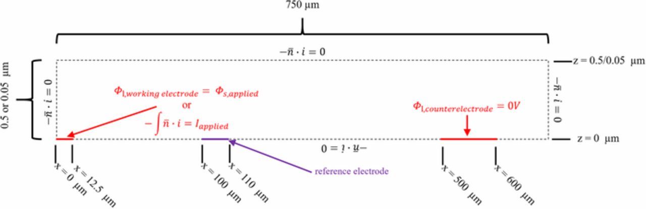
Figure A1. 2-dimensional modeled geometry, not to scale, of the modeled geometries of (A) x-z plane crossing the y = 0 axis from the center of the working electrode (x = 0) to the edge of the chip (x = 750 μm). The working and counter electrodes are solid red and the boundaries of the model are dashed black lines. There is no flux of current along the boundaries of the cells noted by the black dotted lines.
Define variables primary current density distribution Model
The conductivity examined was 3.912 S m−1 which corresponds to 0.1M HBr.46 Temperature was held at 293K. The working electrode was held at 100 mV cathodic potential.
Defined variables secondary current density distribution Model
Variables for this model are shown in Table AI and were exchange current densities (i0) of 3214 A m−2. The exchange current density was chosen to show a Wagner numbers of 0.1. The transfer coefficient was 0.5 for αa and αc. These variables can be found in Table AI. All other variables were the same as the primary current density distribution model.
Appendix. In situ optical microscopy current time transients
Chronoamperometry scans for each overpotential can be found in Figure A2.