Abstract
Perovskite La0.9Sr0.1Ga0.9Mg0.1O3-δ (LSGM) is one of the fastest known oxide ion conductors, with reported enhanced p-type electronic transference numbers at grain boundaries, attributed to space charge effects. As this material is applied as a solid oxide fuel/electrolysis cell electrolyte, it is of interest to learn how its mixed conductivity may be tailored. Field assisted sintering technique/spark plasma sintering (FAST/SPS) and conventional sintering without field or pressure were employed to prepare pellets with various grain sizes, in order to systematically assess the influence of processing route on the mixed conductivity. AC-impedance spectroscopy and the brick layer model were applied to determine local conductivities as a function of temperature, oxygen partial pressure, and dc bias. With increasing sintering temperature and grain size, the following trends were observed: larger electrical grain boundary (GB) widths, higher GB potentials, lower specific GB conductivity, greater dc-bias dependence of GB conductivity, higher pO2-dependence of GB conductivity indicating higher electronic transference numbers, and lower pre-exponential factor for specific GB conductivity. These results suggest an increasing GB space charge effect with increasing sintering temperature/grain size, which coincided with increasing compositional uniformity by TEM and EDS. The results confirm that sintering route is an important variable for tailoring mixed conduction.
Export citation and abstract BibTeX RIS

This is an open access article distributed under the terms of the Creative Commons Attribution Non-Commercial No Derivatives 4.0 License (CC BY-NC-ND, http://creativecommons.org/licenses/by-nc-nd/4.0/), which permits non-commercial reuse, distribution, and reproduction in any medium, provided the original work is not changed in any way and is properly cited. For permission for commercial reuse, please email: oa@electrochem.org.
Reversible solid oxide cells (R-SOCs) are of interest for their dual energy conversion/fuel cell and energy storage/electrolysis cell capability, with high round-trip efficiency, enabling continuous use of intermittent renewable electricity sources. One degradation mechanism that limits their lifetime is the delamination between the oxygen electrode and electrolyte under electrolysis mode, which has been extensively studied in recent years1–3 and attributed to the high oxygen chemical potential at the oxygen electrode/electrolyte interface.1,4 Recently, Virkar et al. reported that higher electronic conductivity within the predominantly ionically conducting electrolyte would lead to a lower tendency to form a high internal oxygen pressure,5 then demonstrated increased stability of cells containing mixed ionic-electronic conducting (MIEC) electrolytes (e.g., YSZ doped with 8mol% CeO2) compared to cells with a purely ion conducting electrolyte (e.g., YSZ).6 Therefore, an electrolyte permitting a small amount of electronic conduction may be beneficial for stabilizing the oxygen electrode-electrolyte interface in R-SOCs. On the other hand, significant electronic conduction in the electrolyte of SOCs is traditionally avoided, as it can lead to shorting of the cell and lower open circuit voltages. Presumably an optimal electronic transference number (whether homogeneous or spatially varying across the electrolyte) exists to address this trade-off, suggesting that understanding how to tailor mixed conduction of electrolytes is an important research task.
Strontium- and magnesium-doped lanthanum gallate, La1-xSrxGa1-yMgyO3-δ (LSGM), has been widely investigated as a perovskite-structured electrolyte for intermediate temperature (400-650°C) SOCs owing to its superior ionic conductivity and thermo-mechanical and chemical compatibility with various perovskite electrodes.7–9 Compared to well-established fluorite-structured yttria stabilized zirconia electrolytes, which have ionic transference numbers close to 1 across a wide range of oxygen partial pressures,10 LSGM can exhibit non-negligible p-type electronic conductivity under oxidizing conditions.11–13 In LaGaO3, the process of ionic compensation with oxygen vacancies (v••O) for Sr- and Mg-acceptor doping can be presented in Krӧger-Vink notation by:
![Equation ([1])](https://content.cld.iop.org/journals/1945-7111/166/10/F569/revision1/d0001.gif)
In intermediate oxygen partial pressures, a high concentration of oxygen vacancies is essentially fixed by the dopant concentration ([Sr'La] + [MgGa'] = 2[v••O]), which coupled with the high vacancy mobility in the perovskite structure, supports the high oxide ion conductivity. However, under more oxidizing conditions, acceptor doping may result in some electronic compensation, through the oxidation reaction:
![Equation ([2])](https://content.cld.iop.org/journals/1945-7111/166/10/F569/revision1/d0002.gif)
![Equation ([3])](https://content.cld.iop.org/journals/1945-7111/166/10/F569/revision1/d0003.gif)
Then, holes contribute to a low but non-negligible electronic conductivity with a linear dependence on (pO2)1/4 (based on Eq. 3, assuming that the hole concentration is relatively low and therefore the oxygen vacancy concentration is not significantly changing with pO2).
Owing to differences in point defect thermodynamics at/near interfaces vs. in the bulk, the ratio of oxygen vacancies to holes can be inhomogeneous at a microstructural level. For example, in LSGM, grain boundaries have been identified as a site of enhanced electronic transference numbers, i.e., the fraction of conductivity deriving from holes. Park et al. have reported higher electronic transference numbers, in O2, at grain boundaries (∼0.093-∼0.32) compared to the grains (∼0.037-∼0.05), in lightly 1 mol% Sr-doped LaGaO3 with an average grain size of 5.8 ± 2 μm by dc polarization studies and oxygen partial pressure dependent measurements of impedance spectra; the latter measurements yielded the higher transference numbers.14,15 For co-doped LSGM compositions similar to that of the present work (e.g., La0.9Sr0.1Ga0.85Mg0.15O3-δ with an average grain size of ∼80 nm, and La0.9Sr0.1Ga0.87Mg0.13O3-δ with grains <50 nm), limited studies have demonstrated again enhanced electronic transference numbers (up to 0.3 in O2) in the grain boundaries.13,16 These investigations have attributed the locally varying electronic transference number to grain boundary space charge effects.
As shown in Figure 1, in the space charge model, electrical grain boundaries consist of a central grain boundary core (GBC) and adjacent space charge zones (SCZs). The SCZs may be crystallographically similar to the bulk of the grains but differ in terms of defect populations. The GBC in LSGM is thought to be positively charged, resulting in the depletion of positively charged species (e.g., oxygen vacancies, holes) and accumulation of negatively charged species (e.g., electrons, and/or possibly mobile acceptors) in the SCZs. The singly charged electron holes (h•) are depleted less than the doubly charged oxygen vacancies (v••O) in the SCZs; therefore, barring extreme changes in local carrier mobilities, the electronic transference number is expected to be higher in the grain boundary compared to in the bulk of the grains, under oxidizing conditions.13,16 Additionally, since all of the relevant charge carriers under oxidizing conditions are depleted in the SCZs, the local (or "specific") grain boundary conductivity is expected to be lower than that of the grain interiors (the "grain core conductivity"). When such potential barriers are present at grain boundaries, the grain boundary current-voltage behavior can become highly non-linear, if the local grain boundary voltage exceeds the thermal voltage.17–19
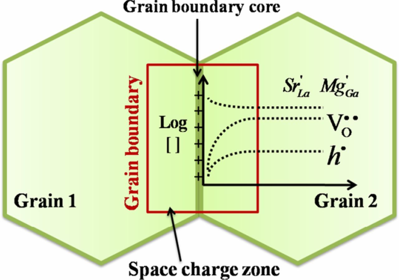
Figure 1. Schematic representation of a grain boundary and grains in LSGM based on space charge model.
The reports mentioned above helped to demonstrate that the grain boundary electrical behavior of high purity LSG/LSGM is consistent with this space charge model. Further support for the space charge model comes from the observed non-linear ("super-ohmic") current-voltage behavior of grain boundaries under high electric fields, studied only in the lightly-doped samples so far.18 On the other hand, Park's more recent study of micro-grained La1-xSrxGaO3-δ suggests that the grain boundary electronic conductivity and moderate grain boundary electronic transference numbers observed for low doping levels become negligible for high doping levels (x > 0.05),20 in contrast to his earlier study mentioned above for nanocrystalline samples with high doping levels. This recent work questions whether the space charge effect is still dominant in highly doped cases, and the extent to which grain size and doping level interact to modify grain boundary structure. Grain boundaries can exhibit blocking behavior to transport for reasons other than (or in addition to) space charge effects, such as current constriction by pores or insulating phases at grain boundaries or structurally-induced charge carrier mobility changes.
Moving forward, further studies of highly doped samples with a range of grain sizes could be beneficial to better understand whether space charge effects play a role in the grain boundary behavior, e.g., via current-voltage measurements, and what magnitude of electronic transference number exists in the grain boundaries. Taken in the context of the existing work, such information can ultimately aid rational tailoring of the grain boundary structure to gain some control over the resulting mixed conductivity. Manipulation of defect equilibria and associated properties, via grain boundary tailoring, is also of significant interest in the broader MIEC perovskite field, where grain boundaries can influence not only ionic/electronic transport but also oxygen surface exchange kinetics. For example, grain boundaries in Sr-doped LaMnO3 have been shown to exhibit higher oxygen surface exchange kinetics and bulk oxygen diffusivity compared to bulk material.21,22 Processing method, microstructure (such as grain size), and composition (such as homogeneous doping contents and heterogeneous local grain boundary chemistry) would be expected to affect the electronic properties in the grain boundaries of perovskites like LSGM, and their study, particularly in the relevant low-to-intermediate temperature range (up to 500°C), would be beneficial to inform design of optimal grain boundary structures. In a variety of other electrolyte materials, grain size has been reported to influence the local or specific grain boundary conductivity,23–26 typically increasing it with decreasing grain size in the nanoscale, via changes in grain boundary space charge potential, local impurity concentrations, and/or other effects. In this work, we therefore applied different processing methods to fabricate pellets with a range of grain sizes at a relatively significant doping level (10% Sr and 10% Mg on the A- and B-sites, respectively), consistent with LSGM used in SOC applications.
Two methods - field assisted sintering technique/spark plasma sintering (FAST/SPS) and pressureless sintering - were applied to prepare highly dense La0.9Sr0.1Ga0.9Mg0.1O3-δ (LSGM9191) pellets with different grain sizes. The FAST/SPS method was chosen because of the benefits of high density and small grain size at a low sintering temperature.27 The ionic/electronic transport was measured by 2-point ac-impedance spectroscopy over a range of temperatures. Equivalent circuit fitting with analysis by the brick layer model (BLM)28 approach was applied to evaluate the electrical responses arising from different microstructural features and to determine average electrical grain boundary widths. The impact of processing route and grain size on grain core (GC), grain boundary (GB), total, and specific GB conductivity was studied. Additionally, the dependence of the conductivities on oxygen partial pressure (pO2) and applied dc bias was investigated to assess any electronic contribution to the conductivity. A space charge model was invoked to estimate the magnitude of grain boundary potential barriers from the measured grain core/specific GB conductivity ratio. The microstructure was evaluated by scanning electron microscopy (SEM) and transmission electron microscopy (TEM), combined with energy dispersive spectroscopy (EDS) mapping and line scans across grain boundaries to evaluate the compositional homogeneity. The results demonstrate tailoring of space charge effects and local electronic transference numbers in LSGM through varying the synthesis conditions and resulting grain size.
Experimental
Pellets fabrication
The La0.9Sr0.1Ga0.9Mg0.1O3-δ (LSGM) nano-powder was synthesized by a modified Pechini method. The stoichiometric amount of starting reactants of La(NO3)2•6H2O (Sigma Aldrich, 99.9%), Sr(NO3)2 (EMD Millipore Corporation, 99.99%), Ga(NO3)3•xH2O (Sigma Aldrich, 99.999%), and Mg(NO3)•6H2O (Sigma Aldrich, 99.999%) were dissolved into distilled water at room temperature in a beaker, followed by adding citric acid and ethylene glycol with the molar ratio of 1 (metals):2:1. The solution was then heated and stirred on a hot plate, at a solution temperature of 80°C. After the polyesterification, the resin was dried at 120°C for 12 h in an oven (EO-300B, ETTAS, Japan). Then the product was gound by agate mortar and pestle, and calcined at 800°C in flowing air for 3 h.
The densification of LSGM powders was performed by two methods, field assisted sintering technique/spark plasma sintering (FAST/SPS) and traditional pressureless sintering. Samples #1-#3 were fabricated by the FAST/SPS method. The densification was performed at 950°C with a holding time of 5 min to obtain dense pellets, with a heating rate of 200°C/min and a pressure load rate of 50 MPa/min. The preload and final pressures were 15 MPa and 100 MPa respectively. Then samples #2 and #3 were annealed (without pressure, in air) at 1200°C for 20 min and 1300°C for 2 h respectively again to achieve larger grain sizes. LSGM pellet #4 was prepared by uniaxial pressing and pressureless sintering. The white powder that resulted from the modified Pechini approach after burning out the solvents was loaded into a 20 mm die, then uniaxially pressed at 125 MPa, and sintered at 1500°C in air for 6 h surrounded by sacrificial powder of the same composition to minimize cation volatilization, with a heating and cooling rate of 3°C/min. Before the electrochemical measurements, the surfaces of all LSGM pellets sintered by FAST/SPS were ground with SiC grinding paper and annealed at 750°C for 8 h in a dry oxygen atmosphere covered by platinum mesh in order to restore the oxygen stoichiometry, due to the strongly reducing environment while performing the FAST/SPS with graphite dies under a high uniaxial pressure.29 Thermal history of the four samples is summarized in Table I.
Table I. Sintering route and nomenclature of the four LSGM samples.
| Sample name | #1-950 | #2-1200 | #3-1300 | #4-1500 |
|---|---|---|---|---|
| Sintering | SPS/FAST at 950°C, 5 min | SPS/FAST at 950°C, 5 min | SPS/FAST at 950°C, 5 min | Sintering with no field or pressure in air at 1500°C, 6h |
| Re-oxidation step | Anneal at 750°C, 8h in dry O2 | Anneal at 750°C, 8h in dry O2 | Anneal at 750°C, 8h in dry O2 | - |
| Grain growth step | - | Anneal at 1200°C, 20 min in air | Anneal at 1300°C, 2h in air | - |
Characterization
The phase purity of LSGM pellets was examined by X-ray powder diffraction (XRD, Rigaku Corp., Japan, Cu kα-radiation). The microstructure and grain size of nanocrystalline and microcrystalline pellets were characterized by scanning electron microscopy (SEM, Hitachi Corp., Japan) and transmission electron microscopy (TEM, JEM-2100HC, JEOL Ltd., Japan). In order to obtain clear SEM images for determining grain sizes, after polishing with polycrystalline diamond suspension (1-9 μm, BUEHLER, USA), thermal etching was performed at a temperature 50°C lower than the final sintering temperature of each sample for 30 min in air before the microstructure characterization. The TEM specimens were prepared by Ar ion milling using Gatan PIPS model 691, with a cold specimen stage, low ion-beam voltages of 0.5–4 keV and small incident beam angles of 3–5° for final thinning to minimize the damage of ion milling on samples. High resolution images near/at different grain boundaries were examined by STEM (JEM-ARM200F, JEOL, Japan) operated at 200 kV, combined with energy dispersive X-ray spectroscopy (EDS) to evaluate the local structure and atomic compositions. The high resolution images of grain boundaries were taken in multiple regions. The average grain size was determined by a line-intercept method (repeated ∼8 times per sample) with the help of Gwyddion image analysis software.
For the electrical measurements, ∼ 20 nm of porous Pt was first sputtered on both faces of each LSGM pellet, and then Ag paste was painted on both faces as porous electrodes. Pt wires were attached with the Ag paste as the current collector. The purposes of the sputtered Pt interlayer were twofold: to prevent Ag paste delamination from the pellet during the measurement and to hinder possible Ag diffusion into the pellets (which however is not expected at significant levels given the low measurement temperatures). We found that without the Pt interlayer, the impedance results were often not reversible, which we attributed to deterioration of the Ag-LSGM interface integrity over time. Two point AC impedance spectroscopy measurements were carried out at 250–450°C in N2/O2 mixtures controlled by mass flow controllers over a range of oxygen partial pressures, with a frequency range of 0.1 Hz to 10 MHz and ac amplitude of 0.5 V, using a Novocontrol Alpha-A impedance analyzer (Novocontrol Technology, Germany). The DC bias measurements were conducted at 21% O2 and pure N2 (pO2 ∼ 0.0012 atm) with a superimposed dc voltage of 0.01-40 V at 250°C and 450°C. The impedance spectra were analyzed by the Zview program (Scribner Associates, USA) to fit the resistance of grain core and grain boundary using an (RQ)(RQ) equivalent circuit (using Boukamp notation).30,31 The average uncertainty in resistance values is estimated as < 5–10%, considering any equivalent circuit fitting or geometry measurement error.
Results
Structural characterization
The final relative densities of LSGM pellets #1-#4 were 96.3%, 97.5%, 91.6%, and 96% respectively. We tentatively attribute the lower density of pellet #3 to the gaseous loss of residual volatile impurities during the pressureless sintering step, which were trapped in the initial pressure-assisted step; this hypothesis is discussed further in the section entitled "Grain boundary conductivity changes vs. microstructure and processing route." Figure 2 shows the diffraction patterns of the densified La0.9Sr0.1Ga0.9Mg0.1O3-δ (LSGM9191) pellets. Two small peaks corresponding to the secondary phase La2Ga4O9 were observed for all LSGM9191 pellets (FAST/SPS and traditional pressureless sintering) and an additional minimal LaSrGa3O7 peak was observed for samples #1-3 (by FAST/SPS method). These are common impurity phases observed in highly Sr- and Mg-doped LaGaO3,32,33 and based on the peak intensities, their volume fraction is estimated to be in the range of ∼2–5%. Previous research has shown that the minor presence of secondary phases did not impact the ionic and electronic conductivities significantly in LSGM.34 We also confirmed by microscopy that these phases appear randomly distributed, rather than occurring solely at grain boundaries, as described further below. Therefore, the slight effect of a small volume fraction of impurity phases was neglected in this study.
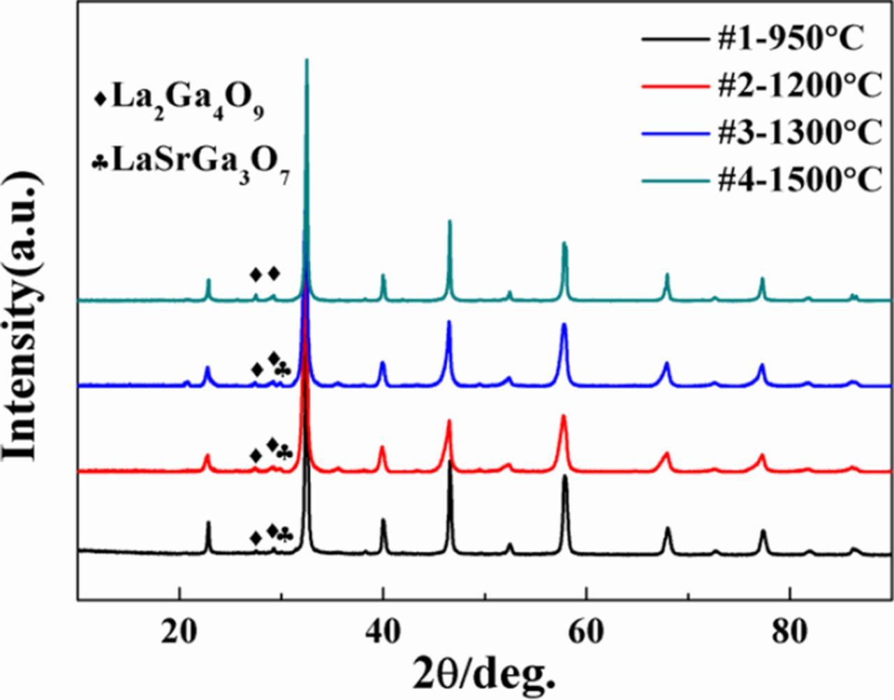
Figure 2. X-ray diffraction patterns of LSGM9191 pellets, prepared at different temperatures and by different methods (SPS/FAST with or without post-annealing at 950–1300°C; pressureless sintering at 1500°C).
The microstructure of representative pieces of the LSGM9191 pellets was examined by TEM and SEM as shown in Figure 3. Sample #1-950°C with an average grain size of ∼98.5 ± 5.9 nm was characterized by TEM with a mild prior thermal treatment at 500°C for 30 min. The average grain sizes of samples #2-1200°C, #3-1300°C, and #4-1500°C were ∼280.9 ± 20.5 nm, ∼649.5 ± 110.4 nm and ∼6.42 ± 0.58 μm, determined by SEM of thermally etched samples, using the line-intercept method. The histograms of grain size distributions of samples #2-4 are also provided in Figure S1. No visible impurity or secondary phase was observed on these samples by SEM; however, the grain boundary morphology of sample #4 appeared slightly different, due to the high thermal etching temperature. The results confirmed the previously-reported benefit of the FAST/SPS method, i.e., smaller grain size at lower sintering temperature with good phase purity and crystallinity.27,35
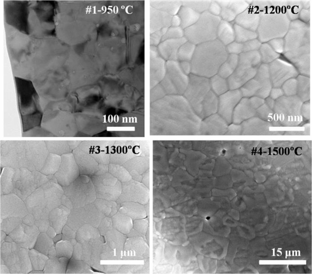
Figure 3. Microstructures of four highly dense LSGM pellets. The average grain sizes are approximately ∼98.5 ± 5.9 nm, 280.9 ± 20.5 nm, 649.5 ± 110.4 nm and 6.42 ± 0.58 μm, using the line-intercept method.
Electrical measurements
Electrical measurements were performed prior to the thermal etching and microstructure analysis. Figure 4 shows typical impedance spectra of LSGM pellets measured at 250°C in 21% O2 atmosphere, consisting of two almost semicircular arcs at high and intermediate frequencies and a more depressed third arc at low frequencies. The black lines represent the fitting for the spectra. These three features are typically attributed to the grain core (GC or bulk, high frequency), grain boundary (GB, intermediate frequency), and electrode (low frequency) responses, respectively. The capacitance of the high frequency arc yields relative permittivity values that are expected for bulk (GC) LSGM,36 and the more depressed shape of the low frequency arc is typical of an electrode response; additionally, the intermediate and low frequency arcs are the most responsive to dc bias (shown later) as expected for interfacial behavior. Therefore, these GC, GB, and electrode attributions seem appropriate.
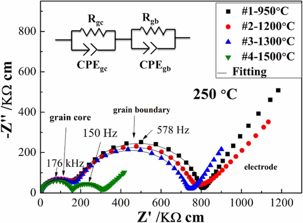
Figure 4. Impedance spectra measured at 250°C under dry 21% O2 for all LSGM9191 samples, corrected for sample geometry. The inset shows the equivalent circuit used to fit the high frequency and intermediate frequency portions of the spectra in this work. CPE means the constant phase element. The black lines represent the fitting.
The high- and intermediate-frequency features of the impedance spectra were analyzed by using a (RQ)(RQ) equivalent circuit (as seen the inset image) in order to extract the GC and GB conductivities. CPE or Q denotes a constant phase element. Because the spectra have been corrected for pellet geometries, each arc diameter is related to its resistivity: GC resistivity or effective (overall) GB resistivity (ρ = RS/L, Ω cm, R is the resistance, S is sample electrode area, and L is sample thickness), because the porosity correction is negligible with such dense samples. As can be seen in Figure 4, a clear difference in the intermediate frequency arc diameter among samples was observed. The effective (overall) GB resistivity decreases monotonically with increasing sintering temperature, as the grain size increases. On the other hand, no changes in GC resistivity were observed by changing the sintering temperature or grain size.
Figure 5 shows the effective conductivities (σ = 1/ρ) as a function of pO2 for dense LSGM pellets with different average grain sizes (∼98.5 nm to ∼6.42 μm). The effective GB conductivity is lower than GC conductivity in the temperatures of interest in all but one condition shown. The repeatable GC and GB conductivity behavior upon lowering and then increasing pO2 confirmed the reversibility of LSGM9191 pellets' behavior at 250°C, 425°C and 450°C. The slight fluctuations (∼4%) at 450°C in Figures 5a, 5c and 5e may have been caused by uncertainty from fitting or slight temperature variations; these fall within our uncertainty estimate of <5–10%. It should be mentioned that the GC arc was absent at high temperature (it lies at higher frequencies than those measured) and therefore the modified fit process could be one of the error sources. As expected from the almost invariant impedance spectra vs. pO2 (not shown), almost no pO2 dependence was found for both GC conductivity and GB effective conductivity in Figures 5a–5f, in which the LSGM pellets were fabricated by the FAST/SPS method. Figures 5g and 4h show GC and effective GB conductivity at different pO2 for #4-LSGM9191 prepared by traditional pressing, measured at 450°C and 250°C, respectively. A positive pO2 dependence was found for the effective GB conductivity while not for the GC conductivity, which is more consistent with the previous reports of acceptor-doped LaGaO3 grain boundary behavior.13 The ionic conductivity is pO2-independent in this range, while the hole conductivity is expected to show a pO21/4 dependence (Eq. 3). From that relationship, electronic transference numbers can be estimated, assuming that the conductivity is purely ionic in the most reducing condition. The grain boundary electronic transference number th.gb (th.gb = 1-σi,gb/σtotal,gb, σi,gb is grain boundary ionic conductivity and σtotal,gb is grain boundary total conductivity) is about 0.067 and 0.034 at a pO2 of 1 atm at 450°C and 250°C for the first series of pO2 change measurements, respectively. However, some apparent decrease of the GB conductivity response was observed during the reverse re-oxidation process, especially for the low operating temperature. Consequently, for that reverse measurement, the th.gb also demonstrated an apparent decrease, which might reflect a kinetic limitation of the redox reaction at low temperatures. To our knowledge, none of the previous studies reported on the reversibility of the GB and GC conductivity under different oxygen partial pressures in LSGM.
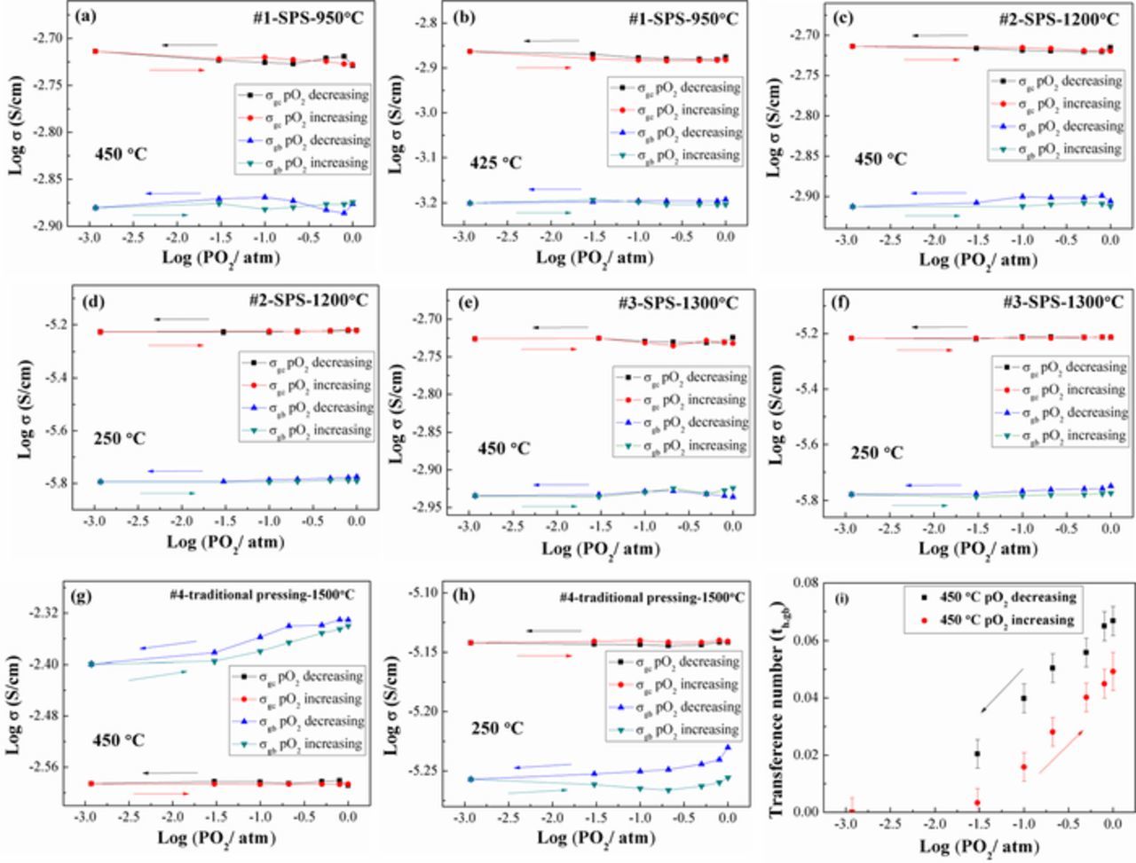
Figure 5. The pO2 dependence of grain core and effective grain boundary conductivity of (a) & (b): #1-950°C, (c) & (d): #2-1200°C, (e) & (f): #3-1300°C, and (g) & (h): #4-1500°C measured at different temperatures, measured first in decreasing pO2 steps and then in reverse with increasing pO2 steps. (i) The electronic transference number in the grain boundary, th,gb, of #4-1500°C measured at 450°C. Note: log indicates log base 10.
The effective conductivities σgc and σgb,eff, total conductivity σtotal, and specific GB conductivity σgb,sp are plotted as a function of temperature in Figure 6. The specific GB conductivity σgb,sp was calculated based on the Brick Layer Model (BLM), given the relatively large grain sizes, and it represents an intrinsic property specific to a single grain boundary rather than the previously shown effective/overall GB ensemble response, which depends significantly on microstructure. (Attempts to apply the nano-Grain Composite Model28 to determine a local GB conductivity without requiring the assumptions of the BLM were less successful given the low GB volume fraction, suggesting smaller grain sizes or wider grain boundaries are needed for LSGM to apply that approach accurately.) The grain boundary width was estimated with the BLM using the equation:
![Equation ([4])](https://content.cld.iop.org/journals/1945-7111/166/10/F569/revision1/d0004.gif)
where dgb, Dg, Cgc, and Cgb are grain boundary width, average grain size, grain core capacitance, and grain boundary capacitance, respectively.34 The obtained GB specific conductivity (σgb,sp) is comparable with previous reports for similar compositions of LSGM prepared by the FAST/SPS method.27 This was calculated from the following equation:
![Equation ([5])](https://content.cld.iop.org/journals/1945-7111/166/10/F569/revision1/d0005.gif)
where σgb,eff is the effective grain boundary conductivity. There was no significant change in grain core conductivity for LSGM9191 vs. grain size in the range ∼98.5 nm to ∼6.42 μm, as shown in Figure 6a. As noted earlier, the effective grain boundary conductivity increases with increasing grain size, although as seen in Figure 6b the effect is most pronounced when transitioning from the SPS/FAST samples to the pressureless-sintered samples with a grain size increase of ∼280.9 nm to ∼6.42 μm. Figure 6c presents the plot of the total conductivities vs. measurement temperature, which exhibits the same trend as that of the effective grain boundary conductivity (6b), suggesting that the effective grain boundary resistance was significantly limiting the total conductivity (σtotal = σgcσgb (σgc+σgb)). As demonstrated in Figure 6d, the specific σgb increased with decreasing grain size, which is consistent with other studies on La0.95Sr0.05Ga0.9Mg0.1O3-δ37 or La0.9Sr0.1Ga0.9Mg0.1O3-δ38 compositions and with reports on other oxide ion conducting electrolyte materials.23,25,26
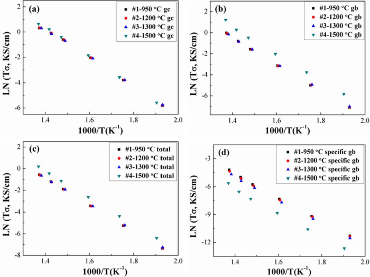
Figure 6. The σgc (a), effective σgb (b), σtotal (c), and specific σgb (d) at different temperatures (250–450°C) for samples with different grain sizes in 21% O2. Y-axis is natural log of conductivity multiplied by temperature, and K represents the temperature unit Kelvin.
The activation energies (Ea, extracted from the Arrhenius conductivity equation σ = (σ0/T)exp ( − Ea/kT)) and the pre-exponential factor (Lnσ0) of each type of conductivity for LSGM are listed in Table II. Only very small differences from sample to sample were observed, which is consistent with the small conductivity changes. The Ea of the effective GB conductivity σgb,eff is higher than that of σgc, which indicates that grain boundaries exhibit higher barriers for the mobility (migration plus dissociation) of charge carriers (consistent with the lower σgb,sp than σgc). For LSGM9191 densified by FAST/SPS, all the Ea slightly decreased with increasing grain size, while microcrystalline sample #4 prepared by traditional pressing demonstrated the highest Ea. The same trend seen with Ea can be observed for the GC, total, and effective GB pre-exponential factors of different LSGM samples, which show a slight decrease when increasing the grain size from ∼98.5 - ∼649.5 nm, while sample #4 exhibited the highest Lnσ0. On the other hand, the pre-exponential factor for the specific GB conductivity showed a monotonic decrease with increasing sintering temperature and increasing grain size among all samples. A number of terms form the pre-exponential factor, including carrier concentrations.
Table II. Conductivity activation energies (Ea) and pre-exponential factors (Lnσ0) for all LSGM samples in 21% O2.
| Sample | σgc / eV | σgb & σgb.sp / eV | σtotal / eV | Ln σ0 (GC) | Ln σ0 (GB) | Ln σ0 (total) | Ln σ0 (GB specific) |
|---|---|---|---|---|---|---|---|
| #1 | 0.97 | 1.09 | 1.06 | 16.03 | 17.23 | 16.26 | 13.04 |
| #2 | 0.96 | 1.08 | 1.04 | 15.87 | 16.99 | 16.06 | 12.70 |
| #3 | 0.96 | 1.07 | 1.04 | 15.72 | 16.95 | 16.00 | 12.36 |
| #4 | 1.02 | 1.11 | 1.06 | 16.89 | 18.60 | 17.00 | 11.72 |
From the measured grain core and grain boundary conductivities, further information about grain boundaries can be inferred. From the BLM Equation 4, electrical grain boundary widths can be estimated, if both the grain core and grain boundary portions of the impedance spectra are present in the frequency range, enabling fitting of both the capacitive and resistive contributions for each. In the present work, this condition was met for only the lowest temperatures (245-323°C), leading to electrical grain boundary widths of ∼1.5, 3.9, 6.8, and 7.3 nm for samples 1–4 respectively; see Figure 7. Further, if the grain boundary blocking effect results solely from space charge carrier depletion, and grain boundaries are treated as back-to-back Schottky barriers, one can estimate the potential at the grain boundary core from the ratio of the specific grain boundary and grain core conductivities:39
![Equation ([6])](https://content.cld.iop.org/journals/1945-7111/166/10/F569/revision1/d0006.gif)
where z = 2 for oxygen vacancies, given predominant ionic conduction, e is the electronic charge, and Δφ(0) is the grain boundary potential relative to the grain core. Applying Eq. 6 to the present data, the corresponding grain boundary potentials similarly increase with increasing grain size/ sintering temperature as well as with increasing measurement temperature, as shown in Figures 7 and 8. Figure 7 also summarizes the main trends observed for the grain boundaries in the four samples, in terms of their grain size: specific grain boundary conductivity increases, specific grain boundary conductivity pre-exponential factor increases, grain boundary width decreases, and apparent grain boundary potential decreases with decreasing grain size / decreasing sintering temperature. There is a pronounced difference in the grain size and grain boundary behavior of the FAST vs. conventionally sintered samples without field or pressure.
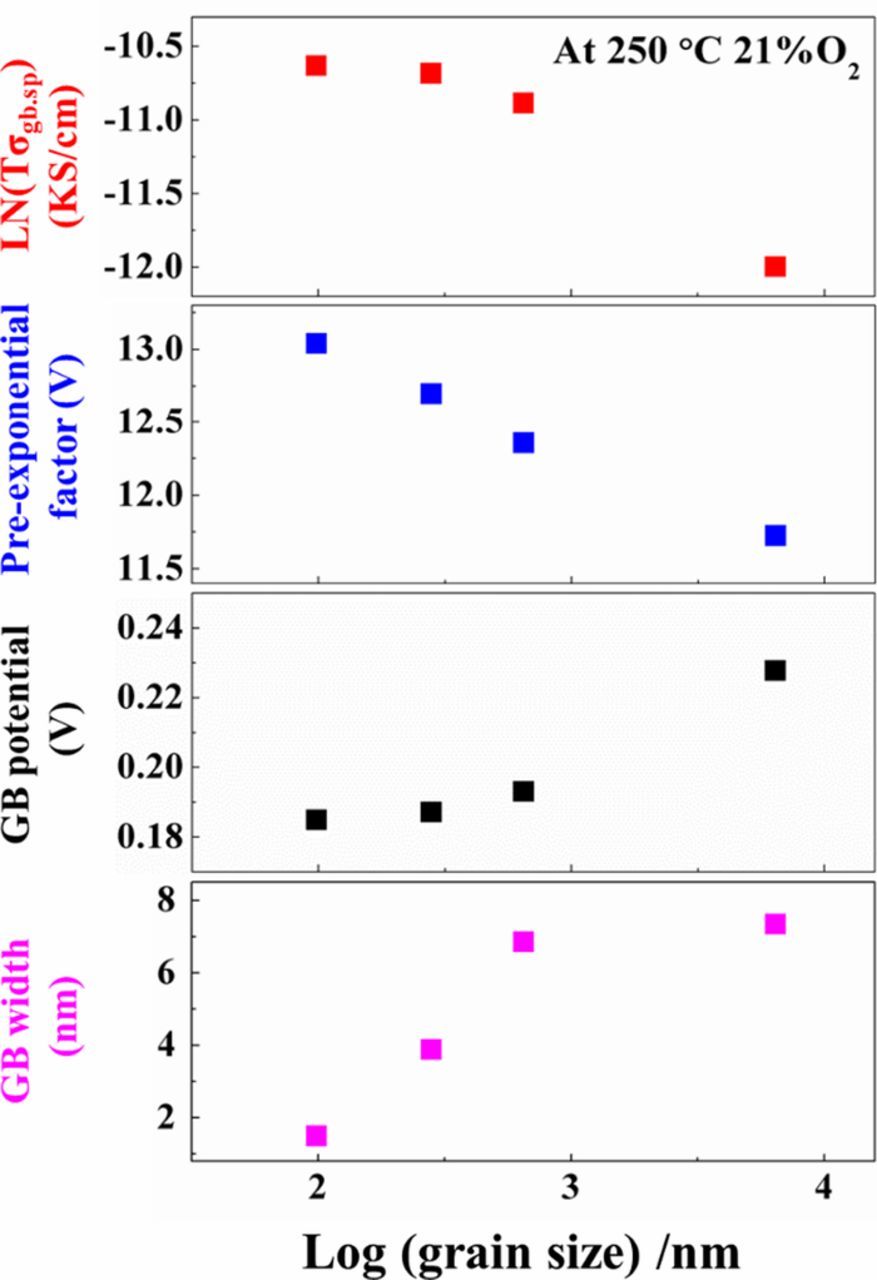
Figure 7. Summary of grain boundary properties as a function of sintering temperature / grain size at 250°C in 21% O2. Top panel: natural log of specific grain boundary conductivity; 2nd panel: specific grain boundary conductivity pre-exponential factor; 3rd panel: grain boundary potential relative to grain core (assuming that grain boundary blocking effects arise solely from space charge carrier depletion); 4th panel: electrical grain boundary width.
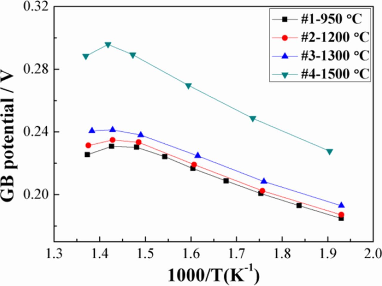
Figure 8. Grain boundary potentials as a function of temperature, estimated from the grain boundary/grain core conductivity ratio, assuming that grain boundary blocking effects arise solely from space charge carrier depletion.
In order to further compare the grain boundary response of LSGM9191 pellets prepared by different methods, their response to dc bias was studied. Nyquist plots of the complex impedance of LSGM pellets #3 and #4 measured at 250°C under different dc bias values ranging from 0.01 V to 40 V (0.052 V/cm – 208.9 V/cm for sample #3 and 0.047 V/cm – 187.1 V/cm for sample #4) are shown in Figure 9. As noted, the diameter of the high frequency arc corresponds to the grain core resistance and the diameter of the intermediate frequency region corresponds to the grain boundary resistance (in this case not corrected for geometry). When dc bias was applied to LSGM pellet #3 (prepared by FAST/SPS), no resistance change was observed in the grain core response, while a limited decrease in grain boundary resistance was observed upon increasing the dc bias voltage, both under 21% O2 and N2, as shown in Figures 9a and 9b. In Figures 9c and 9d, much larger changes in grain boundary resistance were observed for microcrystalline LSGM pellet #4 (prepared by pressureless sintering) under the same dc bias. The larger effect in the microcrystalline sample may be caused by the lower density of grain boundaries in that sample, resulting in a much larger electric field per boundary. In that sample, the dc bias resulted in changes in the grain core response also (Figs. 9c and 9d), which has occasionally been reported for other materials;17 this impedance change recovered slowly after removing the dc bias. A decrease in grain boundary impedance with increasing dc bias is consistent with previous studies demonstrating the existence of a potential barrier at GBs: if we apply a dc voltage, the energy landscape becomes 'tilted' so that for grain boundaries with components normal to the applied field, the barriers become asymmetric in the field,18,19 leading to non-linear current behavior with sufficient voltage. If the local voltage across a given grain boundary is lower than the thermal voltage, the behavior is ohmic, but if the voltage exceeds that value, then the response enters a "super-ohmic" range with a steeper increase in current.
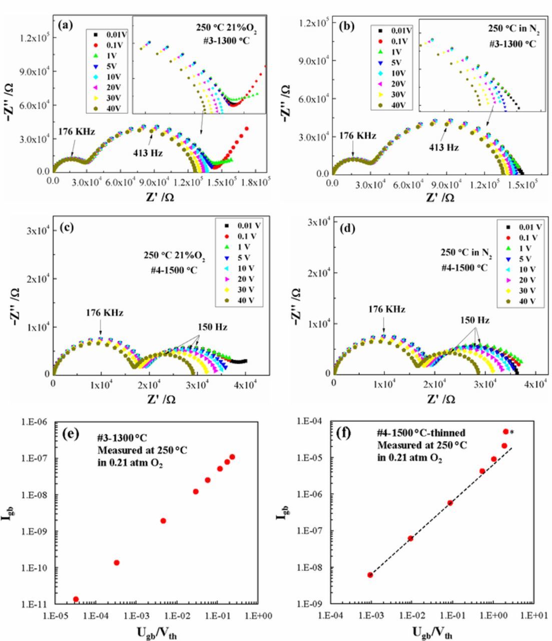
Figure 9. Representative Nyquist plots measured from samples #3 and #4 at 250°C under different dc bias: (a) #3-1300°C in 21% O2; (b) #3-1300°C in N2; (c) #4-1500°C in 21% O2 and (d) #4-1500°C in N2. Grain boundary current-voltage plots for #3-1300°C (e) and #4-1500°C after further thinning (f); dashed line is a guide for the eye showing deviation from ohmic behavior at high voltages; asterisk indicates a point with more uncertainty, given slight distortion in the impedance spectrum. Corresponding impedance spectra for plot (f) are given in figure S3.
From the impedance spectra vs. dc bias it is possible to determine the grain boundary current-voltage behavior.18,19 The grain boundary voltage (Ugb) was determined as:
![Equation ([7])](https://content.cld.iop.org/journals/1945-7111/166/10/F569/revision1/d0007.gif)
Where L/D = Ngb, i.e., the number of grain boundaries across the pellet thickness within the electric field. Then the grain boundary current was determined (Igb) as:
![Equation ([8])](https://content.cld.iop.org/journals/1945-7111/166/10/F569/revision1/d0008.gif)
Figure 9e shows that the grain boundaries of pellet #3 remained ohmic over the full range of dc bias; the power law exponent for the grain boundary current (Igb) vs. the grain boundary voltage (Ugb) normalized to the thermal voltage (Vth = kT/e) was 1.01. Pellet #4 was measured twice; after mechanically thinning it to increase the electric field by a factor of ∼2–3, the sample showed a transition to a "super-ohmic" regime for the highest applied electric fields, as shown in Figure 9f; corresponding impedance spectra are shown in supporting information figure S3. In this case, the power law exponent at low voltages was 1.00 and at higher voltages was ∼1.27–2.10; more data at high voltages would be needed to obtain a more precise value. It is possible to estimate the grain boundary potential from this super-ohmic regime power law exponent (np):
![Equation ([9])](https://content.cld.iop.org/journals/1945-7111/166/10/F569/revision1/d0009.gif)
where fKL is a numerically-determined constant with a value of 0.41±0.05,19,40,41 as long as the grain boundary potential is less than a factor of 12 larger than Vth. This approach yields values of 0.12-0.26 V for pellet #4, which (within the large uncertainty) are consistent with the earlier determined value of 0.23 V (from the conductivity ratio) for this sample at this temperature and gas atmosphere.
Grain boundary microscopy
In order to better understand the variable grain boundary transport behavior in the samples, TEM imaging followed by STEM-EDS mapping and line scans were performed to examine the grain boundary structure and the composition distribution. Figure 10 shows representative high-resolution TEM images of samples #1-950°C, #2-1200°C and #4-1500°C. In these images, the grain boundary zones appear well-ordered with lattice fringes of both grains visible right up to the interface. No obvious secondary phases, nor amorphous/ glassy grain boundary regions are evident. Figure 11 shows the STEM-EDS mapping results of particular (not necessarily representative) regions of LSGM9191 pellets. In these figures, the presence of isolated regions of a Sr-rich secondary phase was observed in both samples #1 and #2 which were prepared by FAST/SPS (Figures 11a and 11b), and some inhomogeneity in Mg distribution is apparent in this particular region of sample #1. The Sr- or Mg- rich regions appear to be limited to isolated second-phase grains, rather than uniformly segregated to grain boundaries. Based on the XRD results of Fig. 2, we understand that these isolated secondary phases are present in all of the samples in similar concentrations but were not captured in all of the particular regions selected for STEM. In addition, small pores (∼20 nm) were found in selected grain core or grain boundary regions of sample #1 (Fig. 11a), although the overall pellet density is still very high. Pores at the grain boundary would affect the measured grain boundary resistance and potentially the electronic transference numbers;42 however, based on our other imaging (not shown), we suggest that such grain boundaries are not representative and would not significantly participate in the current pathway. Very uniform composition was observed in the selected region for sample #4 with a micro grain size which was prepared by traditional sintering, as shown in Figure 11c. Figure 12 shows EDS line scans taken across several grains of sample #1 and across a single grain boundary of samples #2 and #4. Some small regions of enhanced Sr concentration are apparent for sample #1. It is not possible to determine clearly from Figure 12 whether the enhanced Sr concentration corresponds to grain boundary locations or nanoscale secondary phases within grains. Additionally, coupled fluctuations of La, Ga, and O signals across the line scan occur. These latter three concentrations each change in the same way with respect to location, suggesting that the fluctuations of those species may originate in thickness variations. For samples #2 and #4, at least within the spatial resolution and sensitivity of these measurements, no significant cation concentration changes in the grain boundary regions are observed.
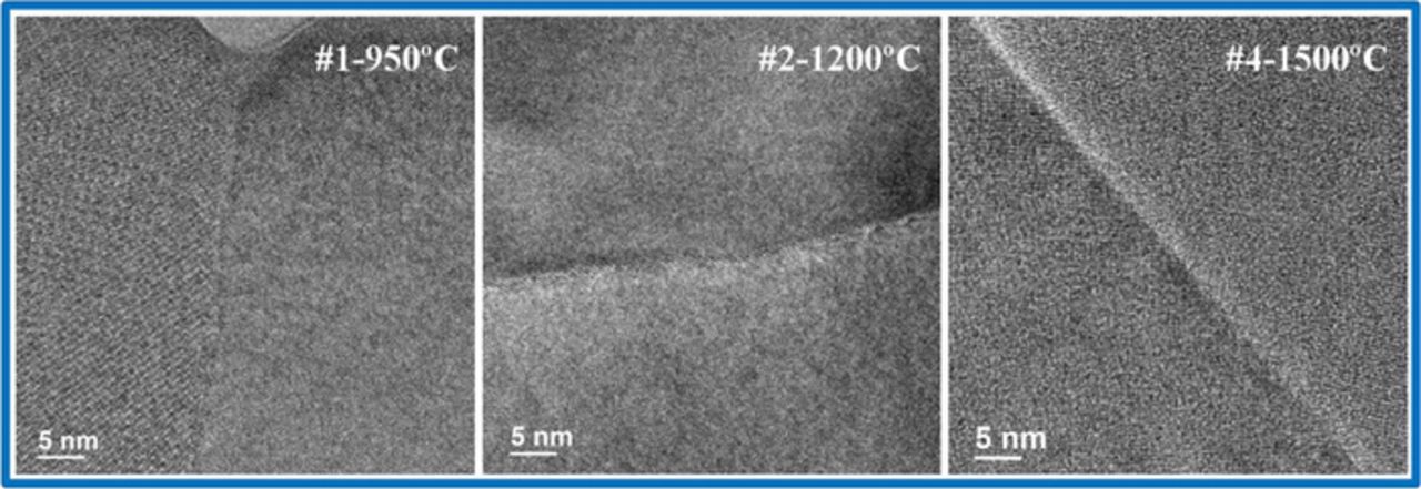
Figure 10. High-resolution TEM images of grain boundaries in three LSGM samples.
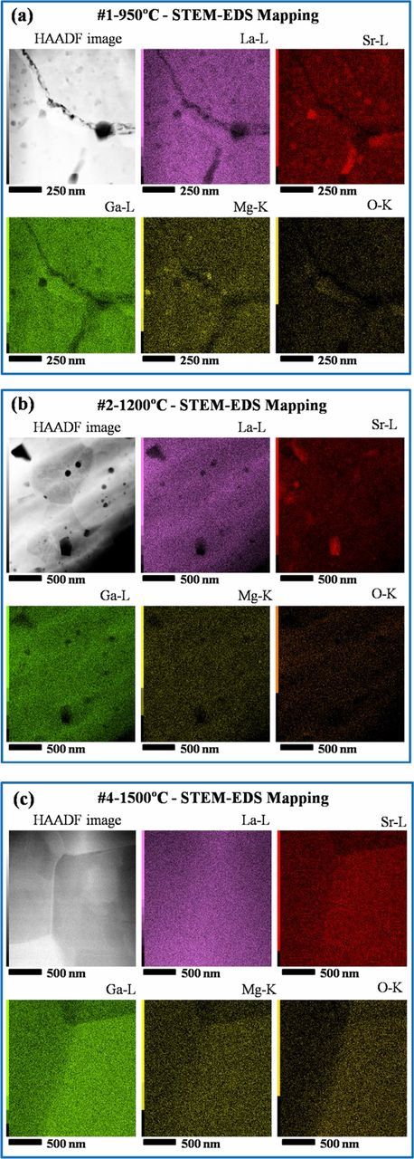
Figure 11. STEM-EDS mapping of selected regions for (a) #1-950°C;(b) #2-1200°C; (c) #4-1500°C
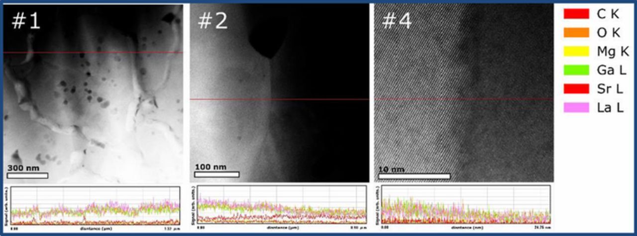
Figure 12. STEM-EDS line scans of three samples. For sample #1 with an average grain size of ∼100 nm, the line scan covers multiple grains, whereas for samples #2 and #4 a single grain boundary is traversed.
Discussion
Grain boundary conductivity changes vs. microstructure and processing route
Systematic changes in electrical behavior took place as the grain size and sintering temperature decreased: total conductivity decreased, effective grain boundary conductivity decreased, and specific grain boundary conductivity increased, while the grain core conductivity remained unchanged. These trends are consistent with other reports of grain size effects in LSGM37,38,43 and in oxide ion conducting electrolytes more broadly.23,25,44 The total and effective grain boundary conductivity changes primarily arise from the increase in grain boundary volume fraction as the grains are smaller at lower sintering temperatures, as grain boundaries are blocking relative to grain cores. The increase in specific grain boundary conductivity with decreasing grain size in other materials has been attributed to a dilution of grain boundary-segregated impurities as the grain boundary volume fraction increases and/or to a decrease in grain boundary core potential.16,24 In the present work, if Schottky barriers at grain boundaries are deemed responsible for the lower specific grain boundary conductivity relative to that of the grain cores, then the calculated grain boundary potential is found to decrease with decreasing grain size (Figs. 7 and 8). On the other hand, compositional inhomogeneity and occasional porosity observed in selected regions of sample #1 might also contribute to the differences in specific grain boundary conductivity. Additionally, it is possible that some residual organic impurities from the nanopowder fabrication process could have been trapped in the grain boundaries of the FAST/SPS samples during sintering, given the applied pressure and confined environment. From thermogravimetric analysis of the calcined precursor powder (Figure 13) it can be seen that there is a small amount of mass loss on heating, which can be attributed to both adsorbed water loss at lower temperatures and organic residue at higher temperatures. Post-annealing of FAST/SPS pellets in a pressureless environment sometimes led to a decrease in their relative densities and appearance of a roughened surface, suggesting internal gas generation, which could arise from trapped volatile impurities. No evidence of residual carbon at grain boundaries was observed by STEM-EDS, however, and so this remains just a hypothesized possibility.

Figure 13. Thermogravimetric analysis showing mass loss of pre-calcined LSGM nanopowder upon heating.
Other changes that were observed with decreasing grain size are suggestive of decreasing space charge effects. Notably, the grain boundary electrical width decreased significantly with decreasing grain size, and the pO2-dependence of the grain boundary conductivity diminished. Additionally, the pre-exponential factor for grain boundary conductivity was the only conductivity-related parameter to monotonically change with grain size, increasing smoothly as the grain size decreased. While the pre-exponential factor contains a number of terms, this trend would be consistent with an increase in charge carriers in the grain boundary, as would be expected from a decreasing space charge effect; i.e., carriers become less depleted as the grain boundary potential decreases.
Limited space charge effects
In the smallest-grained nanocrystalline FAST/SPS samples, the electrical grain boundary widths were quite small, even below 2 nm for sample #1, and there was very little pO2-dependence of the grain boundary conductivity. As the grain size/ sintering temperature increased, there was more evidence of space charge effects, as discussed above. Nonetheless, the magnitude of the effect even in the large-grained case seems to be limited compared to other studies of doped LaGaO3. Grain boundary electronic transference numbers of up to 0.3 have been reported elsewhere,13 compared to the maximum value of 0.067 in the present work. (On the other hand grain boundary potentials of 0.16-0.4 V, increasing with decreasing dopant content, have been listed in other work,13,14 which are not so different from the range of 0.18-0.3 in this work.) The present results therefore raise two questions: 1) Why could space charge effects diminish with decreasing grain size? 2) Why are the space charge effects limited in the present work compared to prior doped LaGaO3 studies?
First, it is expected that the space charge effect may be very sensitive to the concentration profiles of cations, particularly dopants, in the grain boundary regions, which can be influenced by processing route.45,46 For example, at high enough temperatures where dopant cations are mobile, segregation to grain boundaries may occur during cooling in a de-mixing process, if solubility becomes lower as the temperature decreases. The rate at which the sample is cooled will impact the kinetically-limited grain boundary concentration profiles, with implications for local conductivity.16,47,48 Additionally, processes during sintering, such as solute drag, could also in principle lead to changes in cation concentration in grain boundary regions.49 Grain size tends to be coupled to processing variables such as sintering temperature and time in most studies, and so the different processing routes could, in principle, lead to different cation segregation profiles as a function of grain size. Furthermore, the grain boundary chemistry could be affected by the presence of the applied field and pressure in the SPS/FAST technique.50,51 The overall doping concentration could also play a role in the availability of dopants to segregate to grain boundaries and in modifying the equilibrium space charge profiles via changes in bulk properties such as relative permittivity. Recent work by Park showed diminishing evidence of space charge effects as the dopant concentration increased in Sr-doped LaGaO3. For non-dilute Sr concentrations, small electrical grain boundary widths with no pO2-dependence of grain boundary conductivity were observed in that work, accompanied by possible Sr segregation and/or structural asymmetry adjacent to grain boundaries.20 From a theoretical standpoint, Mebane et al. have shown how space charge profiles can evolve as a function of dopant concentration from the dilute to the non-dilute case.52
Second, the space charge effect must be sensitive to the structure/chemistry of the grain boundary core, determining the grain boundary potential. The positive grain boundary potential in LSGM has been attributed to trapped oxygen vacancies at the grain boundary core that do not contribute to long range transport. The grain boundary core structure and corresponding trapped oxygen vacancy concentration may plausibly change with grain size and/or temperature during sintering at which structure becomes frozen.
Caveats and limitations in the analysis
There are several limitations in the analysis that should be noted. First, the Brick Layer Model, which was applied to determine specific grain boundary conductivities and grain boundary electrical widths, is based on several simplifications. It treats the microstructure as a uniform array of cubic grains separated by uniform grain boundary layers, whereas in reality there is a distribution of grain sizes in each sample. It neglects conduction along grain boundary paths that lie parallel to the applied field and any spatial variation of conductivity within grain boundary regions. Determination of the grain boundary thickness involves the assumption that the grain core and grain boundary dielectric constants are equal, which may not be the case.16 An alternative approach to the brick layer model for nanocrystalline samples is the nano-Grain Composite Model.28 We applied that analysis to the data for sample #1 with the smallest grain size, but found that the resulting grain core volume fraction was very high. In this condition, the nano-Grain Composite Model is at its limit of applicability; however, the result does suggest that grain boundaries are indeed very thin in that sample, as also determined by the Brick Layer Model approach. In determining the specific grain boundary conductivity and grain boundary potential, we made the assumption that the grain boundary width does not significantly change with temperature. Based on our determination of grain boundary widths in the low temperature range, this seems to be a valid assumption. Finally, it should be noted again that the grain boundary potentials estimated in this work from the conductivity ratio would only be valid if there are no contributions to grain boundary resistance (vs. grain core values) beyond the Schottky barrier-like charge carrier depletion. If there are any other blocking effects, such as diminished mobility or current constriction from pores or impurities, then the potential values will not be representative of the physical processes occurring at the grain boundaries. These other contributions may be present for the smallest grained samples. For pellet #4, the consistency of the grain boundary potential estimated from the conductivity ratio with the grain boundary potential estimated from the dc bias-dependent impedance supports the presence of a space charge carrier depletion origin.
Conclusions
In this work, we sought to understand how the processing conditions and grain size could affect the mixed ionic/electronic conductivity at the grain boundaries of the fast oxide ion conductor La0.9Sr0.1Ga0.9Mg0.1O3-δ (LSGM9191). Pellets with different grain sizes were prepared by two methods, FAST/SPS and traditional sintering without field or pressure at various temperatures after cold uniaxial pressing. The grain core and grain boundary conductivities were investigated as a function of oxygen partial pressure, temperature, and dc bias by ac impedance spectroscopy. Grain size did not affect the grain core conductivity, while the effective grain boundary and total conductivity increased with grain growth. By applying the brick layer model to interpret the data, the specific grain boundary conductivity of LSGM was shown to be significantly lower than the grain core conductivity and to increase upon decreasing the grain size from ∼6.4 μm to ∼100 nm. Correspondingly the pre-exponential factor for specific grain boundary conductivity increased. In this same range, the electrical grain boundary width decreased with decreasing grain size, and the estimated grain boundary potential (invoking a space charge interpretation of the blocking effect) also decreased with decreasing grain size. The grain boundary conductivities of pellets (#1-#3) prepared by FAST/SPS with different grain sizes due to post-annealing (ranging from ∼98.5 nm to ∼649.5 nm) did not exhibit a clear pO2 dependence, while a pellet prepared by traditional sintering without field or pressure (∼6.42 μm grains) did show a slight pO2 dependence, indicating partial hole conductivity in the grain boundaries with a maximum grain boundary electronic transference number of 0.067 in these conditions. The response of the grain boundary resistance to different dc bias values (0.01 V- 40 V) in N2 or 21% O2 atmosphere was smaller for sample #3 (∼650 nm) compared to sample #4 (∼6.4 μm). When all these results are taken together, they suggest that a space charge effect is present in the sample with largest grain size, enabling local mixed conductivity, and the space charge effect diminishes as the grain size decreases / sintering temperature becomes lower. The space charge effect overall was smaller to that reported in some work with more dilute doping of LaGaO3, suggesting that the high dopant concentration in the present work is partly responsible.
In order to understand these changes, TEM and STEM-EDS mapping were performed on samples #1-950°C, #2-1200°C, and #4-1500°C. All high resolution TEM images showed "clean" grain boundaries with no evidence of significantly amorphous or disordered grain boundary phases. On the other hand, the STEM-EDS mapping showed isolated areas of cation inhomogeneity (e.g., Sr-rich phases, nanoscale Mg-rich areas) and small pores both in grain core and grain boundary regions of samples prepared by FAST/SPS (#1 & #2), suggesting that the grain boundary conduction and space charge effects may be impacted by these local inhomogeneities; nonetheless, given their expected blocking/constricting effect, we do not expect such regions to dominate the current pathway. The results underline the understanding that factors such as grain size, doping level, grain boundary chemistry, and processing routes are interconnected variables that can be adjusted to tailor mixed conduction in LSGM for R-SOC applications.
Acknowledgments
This research has been primarily supported by the U.S. NSF and by JSPS through a Partnerships in International Research and Education (PIRE) Program (NSF grant # 1545907). TC acknowledges a JSPS Doctoral Fellowship (# 201702103). GFH acknowledges a JSPS Kakenhi Grant-in-aid for Young Scientist (B) Award (No. JP16K18235), Progress-100 funding for Kyushu University-MIT-collaboration, and KS and GFH acknowledge the Center-of-Innovation program. NHP, TC, GFH, and KS would also like to acknowledge the support of the International Institute for Carbon Neutral Energy Research (WPI-I2CNER) sponsored by the Japanese Ministry of Education, Culture, Sports, Science and Technology.
ORCID
Kazunari Sasaki 0000-0002-3174-9087
Nicola H. Perry 0000-0002-7207-2113