Abstract
Surface electrical characterization of metals and semiconductors with extensive geometry continues to be of interest. This work explores the electrical information that can be extracted from the electrokinetic (zeta) potential of metallic surfaces, and proposes an analytical model based on streaming potential/current data. In particular, our study focuses on the alloy Ti6Al4V, which is capable of modifying its surface electrical properties after excitation with ultraviolet irradiation due to the semiconductor properties of its TiO2 passivation layer. Evidence is presented for the first time of electronic activity inside the passivation layer following UV excitation. Charge displaced through sample (Q), electrons density (evol), surface charge density (σ) and current density (J) are extracted from the proposed model. The amount of displaced charge through Ti6Al4V disks not exposed to UV irradiation was similar to that displaced inside the thin TiO2 excited layer. Relative conductivity of the TiO2 excited layer versus Ti6Al4V showed a difference of up to five orders of magnitude between the two samples. The model is suitable for application to any metal and any excited semiconductor, thus increasing the usefulness of electrokinetic characterization based on streaming potential/current measurements.
Export citation and abstract BibTeX RIS

This is an open access article distributed under the terms of the Creative Commons Attribution 4.0 License (CC BY, http://creativecommons.org/licenses/by/4.0/), which permits unrestricted reuse of the work in any medium, provided the original work is properly cited.
Relevance of the electrical surface charge
Zeta potential is one of the most important magnitudes to determine stability of suspensions in different industries, such as ceramic casting, cements and plaster, brickmaking and pottery, paper coatings, catalyst supports, water treatment and food processing, amongst others. Rani et al.1 have recently reported, in environmental sciences, that photocatalytic degradation of toxic phenols from water using bimetallic metal oxides increases as the negative zeta potential of the oxides is greater. In the food industry, zeta potential also plays a fundamental role in the quality control of new nanoparticles designed for the encapsulation of active substances2 or in molecular studies involving proteins such as ovomucin.3 In marine science, in the absence of macromolecular interactions, adhesion forces between sea-water bacteria and titanium surfaces are governed by (unspecific) electrostatic interactions,4 which are stronger in the areas of the titanium surface with a higher amount of microstructures.
It is also known that electrical surface charge has an important influence on bioadhesion processes on the surface of medical devices. In particular, electrical interactions can promote osseointegration and prevent bacterial colonization of an implant surface. Lee et al.5 have recently demonstrated that grafting of different polymers on PMMA (Poly(methyl methacrylate)) was effective against bacterial adhesion because these coatings increased the negative surface charge of PMMA and so caused coulomb repulsion between the negatively charged bacteria and the grafted surfaces. Teranaka et al.6 have also reported that zeta potential was involved in the generation of polymicrobial biofilms on mirror-ground oral materials. With regard to osseointegration, Aminian et al.7 have shown that modification of alumina and zirconia surfaces with alkaline phosphatase made the surfaces more negatively charged and more hydrophilic, which resulted in greater cell adhesion, more pronounced cell spreading and a higher number of focal contact points. Electrical interactions, or more specifically small surface currents, are also likely to be behind bactericidal effect and improved osseointegration presented by the surface of the biomaterial Ti6Al4V after irradiation with ultraviolet light. This electronic activity inside the UV-excited TiO2 passivation layer on the Ti6Al4V has not yet been quantified and therefore cannot be specifically attributed to the bactericidal effects of the titanium alloy after excitation.8
Large vs. colloidal electrical surface characterization of materials
In most applications, electrical characterization of surfaces is performed on samples in colloidal form, using electrophoresis to obtain the electrical interaction potential or zeta potential of the samples. However, electrical charge is also of importance in other fields where it works on a large surface area. This is the case, for example, of membranes used in ultrafiltration processes or biomaterials for the manufacture of medical devices. A recent publication has reported in this respect that zeta potential measurements are widely used for the characterization of colloidal suspensions, but have scarcely received attention in the study of large solid surfaces.9 It is not only the composition of the bulk which influences the electrical properties of the surface, but also the geometry of the material. Small spherical-like particles and extended surfaces made from the same material can have different electrical surface properties,10 and for this reason, electrical characterization of a material must be carried out with samples whose geometry is as close as possible to the real situation of its final use.
Bearing this in mind, it would appear from the literature that there are two aspects which need to be improved for characterized surfaces to better reflect the system they represent:
- (i)The electrical information of large surfaces, through zeta potential, is often assumed to be similar to that obtained from the same materials but in colloidal format. Schulz et al.,11 for instance, assumed that the electrical information of flat films (13 mm) was the same as that of 50 μm particles made from the same material when studying the influence of the surface charge of large poly(amidoamine)-alginate hydrogels in adhesion and proliferation of human mesenchymal stem cells. Dwivedi et al.12 also performed an interesting study in which they first electrically characterized through zeta potential vancomycin-loaded niosomes and then coated the surface of large medical devices (bone plates) with these nanoparticles to control bacterial colonization and biofilm formation, finding that the electrical information obtained for the niosomes was close to that of the large coated surfaces.
- (ii)The extended-large surfaces characterized in the literature are usually dielectric surfaces: polymers, glasses, ceramics, etc.13–15 with minimal information on conductive surfaces. In particular, it is difficult to find information on the surfaces widely used in the manufacture of orthopaedic devices such as titanium or its alloys. Electrical characterization of large metallic surfaces through zeta potential is not well understood, probably because of the particularities of streaming potential and streaming current techniques.16 As reported in the work of Roessler et al.,17 electronic conduction of metal had an influence on the overall value of the measured streaming potential while operating with an electrokinetic analyser, which resulted in different zeta potential values from those obtained from streaming current. Underestimation of the zeta potential from streaming potential was then directly related to the conductivity of the metal in another study carried out by our group,16 leading us to recommend determination of the zeta potential through streaming current, rather than streaming potential measurements.
Continuing the above research, we explored how electrical information about the bulk metal could be obtained from the underestimated value of the streaming potential, and within this framework, the objectives of the present paper were established.
The first objective was to quantify, for the first time, the electrical contribution of the bulk metal to the measured value of the streaming potential. We then proposed a new model of electrical analysis which would permit the determination of magnitudes such as surface charge density, displaced charge, volumetric density of displaced charge and current density inside the metallic samples. The model has been validated using Ti6Al4V and aluminum and can be used to detect, for the first time, the huge electrical change that the TiO2 passivation layer of the alloy undergoes after excitation with UV light.
Materials and Methods
Dielectric samples and L/Q factor determination
Three dielectrics were employed: Poly(methyl methacrylate) (PMMA), borosilicate glass and polydimethylsiloxane (PDMS). Two disks of 25 mm diameter were used in each experiment to configure the electrokinetic channel.
We used the dielectrics to obtain the geometrical factor of the cell. Briefly, the geometrical factor is defined as the ratio between the channel length (L) and the cross section of the electrokinetic channel (Q): L/Q. It provides information on the compression of the channel and, since the electrokinetic cell is adjustable, it should be maintained constant to achieve a better comparison between the results from the different samples. We monitored channel compression level by plotting pump voltage versus pressure (p) between both ends of the electrokinetic channel. Equal plots guaranteed the same compression inside the electrokinetic channel, and therefore the same flow path. In the electrokinetic analyser software (EKA, Anton Paar), this process is called "flow check". Calculations made with dielectrics were transferred to the conductor samples under the same flow check conditions.
To obtain the value of L/Q, the electrokinetic cell resistance (Rcell) was obtained through the ratio between Vstr (streaming potential) and Istr (streaming current),16 which accounts for the conductivity of the flow path (Kcell).
![Equation ([1])](https://content.cld.iop.org/journals/1945-7111/166/16/H871/revision1/d0001.gif)
The value of Kcell was taken as that of the electrolyte (liquid conductivity). Theoretically, an electrolyte with high ionic strength should be used to obtain a liquid conductivity higher than the surface conductivity of the sample (in the case of dielectrics). This is guaranteed in 10−1 M KCl but the limit for neglecting surface conductivity versus liquid conductivity can be established at 10−3 M.16 We made estimations of L/Q by using both ionic strengths: 10−1 M and 10−3 M. The values of L/Q were similar but in the case of 10−1 M the dispersions of streaming potential (Vstr) and streaming current (Istr) were very high, and so it was necessary to analyze the plots of Vstr-p and Istr-p in sections, by considering only the slope of the section where ΔVstr or ΔIstr had a clear linear relationship with Δp.
With this information, the average L/Q value used in this work is 5369 m−1. The liquid conductivity values, Kcell, ranged between 17–19 mS/m.
Metallic samples and electrical information from streaming potential and current
We performed the electrical analysis with three different metallic materials: Ti6Al4V (disks of 25 mm diameter, 2 mm thickness), aluminum (disks of 25 mm diameter and 1.36 mm thickness) and UV-irradiated Ti6Al4V (UV-Ti6Al4V) (disks of 25 mm diameter, 2 mm thickness). In the case of Ti6Al4V, the spontaneous passivation layer on its surface, mainly composed of amorphous TiO2,18 was taken into account. This layer, with about 5–10 nm thickness, has semiconductor properties and can be activated under irradiation with UV-C light. In the present work, we carried out activation using a Philips UV lamp of 257 nm wavelength for 15 h, as previously described.8
To clarify the presentation of results, we analyzed the metallic samples with two comparison groups:
Ti6Al4V versus aluminum (Group 1)
Ti6Al4V versus UV-Ti6Al4V (Group 2)
Ti6Al4V was used as reference in both comparisons. The first group (Ti6Al4V versus aluminum) was used to validate the electrical model. The second group was used to evidence the electrical changes occurring on the Ti6Al4V surface after irradiation with UV light.
As previously stated, we measured the streaming current to obtain the real zeta potential of the metallic samples from the following expression:16
![Equation ([2])](https://content.cld.iop.org/journals/1945-7111/166/16/H871/revision1/d0002.gif)
ɛr, ɛ0 and η being relative permittivity of the electrolyte solution, vacuum electric permittivity and solution viscosity. Since the compression of the electrokinetic channel was equal to that of dielectrics (same flow check), L/Q value was taken as the value for dielectrics.
dIstr/dp was the slope of the streaming current (Istr) vs. pressure (p) plot. Pressure was applied in a differential form (ramp form) from 0 to 600 mbar.
The value of ζ from Equation 2 was used to obtain the real value of the streaming potential (Vstr-real) and this was compared to the value measured with the EKA system (Vstr).16 Thus,
![Equation ([3])](https://content.cld.iop.org/journals/1945-7111/166/16/H871/revision1/d0003.gif)
In order to obtain absolute values of the measured streaming potential (Vstr) and to relate them with the values of Vstr-real, curves of Vstr vs. p were displaced to the zero origin after being fitted to a straight line (R2 always close to 1).
The difference between Vstr-real and Vstr was the potential difference between the extremes of the metallic disk as a consequence of the electronic displacement inside the metal disks during the streaming potential measurement process in the EKA (Vmetal). That is to say:
![Equation ([4])](https://content.cld.iop.org/journals/1945-7111/166/16/H871/revision1/d0004.gif)
Vmetal has not been previously quantified and its value can be related to the electric field generated by the electronic density accumulated at both extremes of the metallic disks. This information was the starting point for the electric field model that we propose.
Electric field model
Fig. 1a shows a schematic representation of the charge distribution proposal inside the metallic samples. EKA operation under the streaming potential option (open circuit) generated electronic displacements inside the two metal disks which made up the electrokinetic channel. These electron movements provoked the accumulation of charge at both ends of each disk and, consequently, a new potential difference appeared, Vmetal. The measured potential difference between the electrodes (Vstr) was affected by this electronic distribution and so the real streaming potential (Vstr-real) was expressed as the sum of Vstr and Vmetal (Equation 4).

Figure 1. Schematic representation of: (a) charge distribution at both ends of each one of the metal disks which make up the electrokinetic channel under streaming potential (Vstr) operation. Vmetal is the potential difference between the two ends of the metal disks due to the electronic displacements inside the sample; (b) top view of the charge distribution at one end of the metal disk which makes up the electrokinetic channel, d and L being the width and length of the charged strip; (c) Schematic representation of the electric field differential element (dE) due to a charge differential element, dq, of a charged line, at a point P located in the bisector line.
As can be seen, both ends of the disks closest to the electrodes become charged with the opposite charge due to the electron movement inside the metal, that is, each metal disk becomes polarized and a surface charge distribution appears at each end of the disk.
In the approximation used in this study, we assume that each surface charge distribution has the height of the disk thickness, represented by "d", and a small width, represented by "L", as in the scheme in Fig. 1b.
If L is small, the curvature is also negligible and can be approached to a thin rectangular strip with dimensions d*L. This strip can also be considered to consist of many segments of L lengths.
The electric field caused by any charged segment along the bisector line (Fig. 1c) is given by:
![Equation ([5])](https://content.cld.iop.org/journals/1945-7111/166/16/H871/revision1/d0005.gif)
λ being the linear charge density along the segment, x the minimal distance from the segment to the point where the electric field is calculated, and θ the angle represented in Fig. 1c.
This electric field is directly related, through the gradient function, with the potential difference between two points.
![Equation ([6])](https://content.cld.iop.org/journals/1945-7111/166/16/H871/revision1/d0006.gif)
By relating x with θ:
![Equation ([7])](https://content.cld.iop.org/journals/1945-7111/166/16/H871/revision1/d0007.gif)
Thus setting the reference potential far from the segment where θ ≈ 0°, then
![Equation ([8])](https://content.cld.iop.org/journals/1945-7111/166/16/H871/revision1/d0008.gif)
In the case of a strip of length L and width d, the strip can be assumed to be composed of many segments of the same length distributed in a continuous form. If d is small in comparison to the distance x, where the electric field is calculated, the electric field can be said to be the sum of the electric fields due to the infinite segments inside the strip, so:
![Equation ([9])](https://content.cld.iop.org/journals/1945-7111/166/16/H871/revision1/d0009.gif)
σ being the surface charge density of the strip.
Consequently, the potential can be expressed by:
![Equation ([10])](https://content.cld.iop.org/journals/1945-7111/166/16/H871/revision1/d0010.gif)
The potential difference between the two ends of the disk is the difference between the potential at the positive end (V+) and the potential at the negative end (V−) and both potentials are obtained through the Equation 10. Consequently, Vmetal is equal to this potential difference,
![Equation ([11])](https://content.cld.iop.org/journals/1945-7111/166/16/H871/revision1/d0011.gif)
Then if Vmetal is known from Equation 4, it would be possible to obtain the surface charge density (σ) accumulated at both ends and, consequently, the charge (electrons) displaced through the metal (Q), the volumetric displaced electrons density (evol) and the current density inside the conductor (J).
![Equation ([12])](https://content.cld.iop.org/journals/1945-7111/166/16/H871/revision1/d0012.gif)
![Equation ([13])](https://content.cld.iop.org/journals/1945-7111/166/16/H871/revision1/d0013.gif)
![Equation ([14])](https://content.cld.iop.org/journals/1945-7111/166/16/H871/revision1/d0014.gif)
![Equation ([15])](https://content.cld.iop.org/journals/1945-7111/166/16/H871/revision1/d0015.gif)
t being the time and S the cross section of the conductor.
Although exact quantification of the above magnitudes: σ, Q, evol, J, is impossible because they are based on the electrical model and exact quantification of parameters such as L, comparisons between samples provide valuable information. Deviations from this assumption would introduce certain variations to the specific value of the electric field in any conductor, although comparisons between samples would not be affected.
In particular, θ (directly related with L) in the calculations of V+ and V− was taken as 5°, which gave an L value of about 4 mm (x = 25 mm, diameter of the disks). Calculations with higher angles such as 10°, or lower such as 2°, did not produce significant changes in the relationships obtained (data not shown).
Operation with EKA
The EKA was operated in a pressure ramp form, from 0 to 600 mbar. Within each measurement, the direction of the flow was changed alternately (10 times in total) to avoid accumulation of charge on the electrodes. Experiments were carried out with 10−3 M KCl electrolyte. Streaming potential and streaming current were measured for both dielectrics and metals. Two disks of 25 mm diameter, in parallel form, made up the electrokinetic channel of the cell. At both ends of the electrokinetic channel there were two aligned silver electrodes. These electrodes were chlorinated (coated with AgCl) prior to each experiment to discard any deterioration of the AgCl coating layer. They were also short-circuited for 24 h in 10−3 M KCl to avoid any residual potential difference between them, so that measurements gave only electrical information from the electrokinetic cell.
We exported the data on Vstr vs pressure to an Excel sheet to make the corrections as outlined previously. We then adjusted the data to a straight line, ignoring fluctuations at low pressures (almost always data between 0 and 100 mbar) and made corrections so that zero coincided with the origin of the ordinates. Only under these conditions were the results of all experiments comparable. The values of Vstr were different at any selected pressure but the comparative analysis at each pressure always showed the same trend and, therefore, the same conclusions. Any pressure (avoiding initial values) could be chosen for future study. We present two values in this work, those obtained at 300 mbar and at 500 mbar. The 300 mbar value was sufficient to guarantee stability of the measurement from the outset, and 500 mbar was close to the end of the measuring process, with high stability.
We repeated the experiments at least three times to confirm the results. Repetitions implied the preparation of new electrolyte, new chlorination of the electrodes, and new pairs of samples.
Results and Discussion
Group 1: validation of the model
Table I shows the absolute values of Istr and Vstr from EKA of Group 1 at 300 mbar and 500 mbar. The calculated values of Vstr-real and Vmetal from Equations 3 and 4 are also given.
Table I. Absolute values of measured streaming current (Istr) and streaming potential (Vstr). Real streaming potential value (Vstr-real) obtained from streaming current and calculated potential difference between the ends of the metal disks (Vmetal) under the streaming potential operation of EKA.
| Vstr-real | Vmetal | |||
|---|---|---|---|---|
| Metal | Istr [mA] | Vstr [mV] | [mV] | [mV] |
| 300 mbar | ||||
| Ti6Al4V | (6.3 ± 0.3)·10−5 | 5.2 ± 0.2 | 19 ± 1 | 14 ± 1 |
| Aluminium | (1.14 ± 0.06)·10−4 | 13.2 ± 0.7 | 35 ± 2 | 22 ± 2 |
| 500 mbar | ||||
| Ti6Al4V | (1.14 ± 0.06)·10−4 | 12.0 ± 0.8 | 34 ± 2 | 22 ± 2 |
| Aluminium | (1.55 ± 0.07)·10−4 | 19.5 ± 0.7 | 47 ± 2 | 28 ± 3 |
All obtained values were negative, thus indicating the negative charge of the surface inside the electrolyte. Since the sign of the zeta potential is not relevant in the future analysis, because it is based on the changes in the magnitudes, absolute values are easier to work with, and for this reason all the data in the tables are positive.
Results demonstrate the higher values of Vstr-real versus Vstr regardless of the conductor or the pressure. It is of interest to note that the potential difference generated at both ends of the conductors due to electronic conduction was always higher than the measured streaming potential ΔVmetal > Vstr, which reveals the important contribution of electron movements inside the metals during the streaming potential measurements.
As expected, streaming currents and streaming potentials increased with pressure, and consequently so did Vstr-real and Vmetal. This means that electronic currents inside the metals were higher as the pressure increased.
Regardless of the pressure selected, currents and potentials were higher for aluminum than for Ti6Al4V. In particular, the potential difference between the two ends of the metallic disks (Vmetal) was higher for aluminum than for Ti6Al4V and the changes between both metals appeared to be greater at 300 mbar (8 mV) than at 500 mbar (6 mV). In other words, Vmetal for Al was 1.6 and 1.3 (±0.2) times higher than for Ti6Al4V at 300 mbar and 500 mbar, respectively. This result is in agreement with the higher conductivity of aluminum versus Ti6Al4V, KAl = 3.78·107 S/m; KTi6Al4V = 6·105 S/m,19 implying greater capability of aluminum, compared to Ti6Al4V, to internal electronic displacements.
Table II summarizes the magnitudes obtained with the electrical model from the value of Vmetal. Surface charge density at both ends of the disks (σ), displaced charge (Q) and electron density, associated to surface charge density, over the conductor volume (evol) also increased with pressure and were higher for Al than for Ti6Al4V, regardless of the pressure. The differences between Al and Ti6Al4V were similar at both pressures: Δσ≈3 C/m2; ΔQ≈1 C; Δevol≈1.7 e−/m3. The final column of Table II compares the current density between both metals, indicating that electrical activity for Al was double that for Ti6Al4V.
Table II. Magnitudes derived from Vmetal using the electrical model proposed in this study. Surface charge density (σ) accumulated at both ends of the metals, amount of charge displaced through the metals (Q), electrons density (evol) and ratio of current density (JAl/JTi6Al4V).
| Metal | σ [C m−2] | Q [C] | evol [e− m−3] | JAl/JTi6Al4V |
|---|---|---|---|---|
| 300 mbar | ||||
| Ti6Al4V | (2.2 ± 0.2)·10−9 | (1.9±0.1)·10−14 | (1.2 ± 0.1)·1011 | 2.3 ± 0.4 |
| Aluminium | (5.1 ± 0.6)·10−9 | (3.0 ± 0.3)·10−14 | (2.8 ± 0.3)·1011 | |
| 500 mbar | ||||
| Ti6Al4V | (3.5 ± 0.5)·10−9 | (3.1 ± 0.3)·10−14 | (1.9 ± 0.2)·1011 | 1.9 ± 0.4 |
| Aluminium | (6.5 ± 0.7)·10−9 | (3.9 ± 0.4)·10−14 | (3.6 ± 0.4)·1011 | |
Group 2: model on photo-activated TiO2 layer (UV-irradiated Ti6Al4V)
Table III presents the absolute values of Istr and Vstr from EKA and the calculated Vstr-real and Vmetal at 300 mbar and 500 mbar for Ti6Al4V and UV-Ti6Al4V.
Table III. Absolute values of the measured streaming current (Istr) and streaming potential (Vstr). Real streaming potential value (Vstr-real) obtained from streaming current and calculated potential difference between the ends of the samples (Vmetal) under the streaming potential operation of EKA. Samples refer to non-excited Ti6Al4V and Ti6Al4V after irradiation with UV-light (UV-Ti6Al4V).
| Metal | Istr [mA] | Vstr [mV] | Vstr-real [mV] | Vmetal [mV] | Vexcited-TiO2 [mV] |
|---|---|---|---|---|---|
| 300 mbar | |||||
| Ti6Al4V | (6.3 ± 0.3)·10−5 | 5.2 ± 0.2 | 19 ± 1 | 14 ± 1 | 15 ± 2 |
| UV-Ti6Al4V | (1.59 ± 0.06)·10−4 | 14.2 ± 0.3 | 42 ± 1 | 28 ± 1 | |
| 500 mbar | |||||
| Ti6Al4V | (1.14 ± 0.06)·10−4 | 12.0 ± 0.8 | 34 ± 2 | 22 ± 2 | 19 ± 4 |
| UV-Ti6Al4V | (2.59 ± 0.03)·10−4 | 27.8 ± 0.5 | 69 ± 1 | 41 ± 1 | |
Similar to what is seen in Table I, the magnitudes in UV-Ti6Al4V increased with pressure, Vstr-real being always higher than Vstr measured from EKA and Vmetal also higher than Vstr.
On comparing aluminum, Ti6Al4V and UV-Ti6Al4V, the highest absolute Vstr-real was for UV-Ti6Al4V, with a value of 69 mV at 500 mbar. This was also associated to the highest Vmetal for this sample, regardless of the pressure.
The differences between Ti6Al4V and UV-Ti6Al4V must be associated to the electrical changes occurring on the TiO2 layer after irradiation. The difference between Vmetal(Ti6Al4V) and Vmetal(UV-Ti6Al4V) informs about the contribution of the electronic activity inside the excited TiO2 layer after irradiation with ultraviolet light since the irradiation only affects the passivation layer of TiO2. The potential difference between both ends of the excited TiO2 layer is expressed in the final column of Table III and is denoted as Vexcited-TiO2.
The electrical model developed in Materials and Methods to obtain information on the electronic displacements inside the metal from the data of Vmetal can be also applied to the activated TiO2 layer, taking as input value that of Vexcited-TiO2. In this case, the charge distribution at both ends of the TiO2 layer, closest to the electrodes, can be placed close to a strip with a thickness of about 5 nm. Results are collected in Table IV.
Table IV. Magnitudes derived from Vmetal using the electrical model proposed in this study. Surface charge density (σ) accumulated at both ends of the samples, amount of charge displaced through the samples (Q), electron density (evol) and ratio of current density (Jexcited-TiO2/JTi6Al4V). TiO2 layer refers to the passivation layer on Ti6Al4V excited after UV treatment.
| Metal | σ [C m−2] | Q [C] | evol [e− m−3] | Jexcited-TiO2/JTi6Al4V |
|---|---|---|---|---|
| 300 mbar | ||||
| Ti6Al4V | (2.2 ± 0.2)·10−9 | (1.9 ± 0.1)·10−14 | (1.2 ± 0.1)·1011 | (4.2 ± 1.0) ·105 |
| Excited-TiO2 layer | (9.2 ± 1.5)·10−4 | (2.0 ± 0.3)·10−14 | (5.1 ± 0.9)·1016 | |
| 500 mbar | ||||
| Ti6Al4V | (3.5 ± 0.5)·10−9 | (3.1 ± 0.3)·10−14 | (1.9 ± 0.2)·1011 | (3.4 ± 1.1) ·105 |
| Excited-TiO2 layer | (1.2 ± 0.3)·10−3 | (2.6 ± 0.5)·10−14 | (6.7 ± 1.4)·1016 | |
The amount of charge (Q) displaced between both ends of the excited TiO2 layer was similar to that for Ti6Al4V. This charge moves through a much more reduced area than the whole disk of Ti6Al4V and, for this reason, the surface charge densities at both ends of the layer must be much higher than those of the Ti6Al4V disk and so, consequently, must the electronic displacements. As shown in the first column of Table IV, σ(excited-TiO2) was five orders of magnitude higher than σ(Ti6Al4V), regardless of the pressure selected for analyzing the results. These large differences were also evident in the volumetric electronic density evol, responsible for the appearance of the surface charge at both ends of the layer and, similarly, in the ratio between the current density inside the irradiated TiO2 layer as compared to that inside the Ti6Al4V disk (Jexcited-TiO2/JTi6Al4V).
The results of Table IV show, for the first time, the huge electronic activity inside a thin layer of TiO2 after irradiation with UV-C. Conductivity of the TiO2 layer before irradiation was that of a dielectric, in the range between 10−11 and 10−16 S/m (TiO2 material information from Goodfellow Catalogue). However, after irradiation, conductivity of the TiO2 layer changed drastically to that of conductor values. As far as we know, these conductivity values of the excited semiconductor have not been reported in the literature, but we can estimate their values by taking into account the relationship between the current density and the electric field:

at 300 mbar:
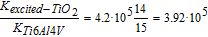
and at 500 mbar:
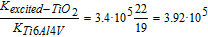
Despite the fact that the above magnitudes are affected by experimental uncertainties (Tables III and IV), it is of interest to highlight the practically identical values obtained in the equations even with input values that depended on pressure. This is what was expected, since the ratio between the conductivities should be intrinsic to the materials and not dependent on surface charge distribution due to the electric field model or on the Vmetal obtained from a specific pressure. This is an indication, therefore, of the reliability of the model developed in this research and of how the data should be analyzed. Consequently,
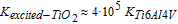
Conductivity of the passivated layer of TiO2 on Ti6Al4V, after irradiation, became five times higher than that of the Ti6Al4V bulk. This result reinforces the idea that the semiconductor was still activated after the ultraviolet lamp was disconnected, and that this electronic activity must be behind the bactericidal effects described for the irradiated Ti6Al4V biomaterial.20 The electrical changes are also in agreement with the previous electrochemical impedance spectroscopic (EIS) results where EIS and Mott-Schottky plots showed that UV treatment caused an initial increase on the surface electrical conduction of this material. In addition, EIS and polarization plots indicated higher corrosion currents at the UV treated surfaces, compared to the non-irradiated samples.21 In line with these results, Deng et al.22 have reported recently that UV-illumination stimulated the nano-TiO2 semiconductor with elevated conductivity in favor of passing corrosion current.
The study of the properties of TiO2 is an issue of great interest in the research community. It is also true that most research focuses on the study of TiO2 nanoparticles with direct application to the manufacture of batteries, solar cells, biosensors, water treatments, cosmetics, etc.23–25 Other applications include neurosciences and the textile industry.26,27
Excitation of TiO2 is key in many of these applications and therefore we consider that it is of great importance to obtain maximum information from the excited state of TiO2. It has been confirmed both by previous works and by this research that excitation of TiO2 is not something instantaneous that disappears when the irradiation ceases but that it is maintained in time and the electrical changes associated with this fact are measurable. For the first time, electrical properties are quantified and the conductivity value of this excited state of TiO2 is provided.
Conclusions
An electrical model to obtain information on the electronic activity inside metals and excited semiconductors while operating under streaming potential-based electrokinetic conditions has been proposed and validated. The model is suitable for application to any metal and any excited semiconductor, thus increasing the usefulness of electrical characterization based on streaming potential and streaming current.
For the first time the value of the conductivity of a thin excited TiO2 film after irradiation with UV light is estimated.
Acknowledgment
The authors gratefully acknowledge financial support from "Ministerio de Economía y Competitividad" (PCIN-2016-146, MAT2015-63974-C4-3-R and RTI2018-096862-B-I00) and "Junta de Extremadura-FEDER: European Regional Development Fund" (IB16117, GR15089 and GR18153). We are grateful to James McCue for assistance in language editing.
ORCID
M. Luisa González-Martín 0000-0002-9207-444X