
Abstract
We found using UV-curable polymer (NOA63 from Norland Optics) film as a passivation layer, which was very simple and convenient to perform, could provide a temporary barrier for the organic light emitting devices (OLEDs). The NOA63 protective layer significantly restricted the moisture that penetrated into the OLEDs, but did not affect its luminescent characteristics. The decay time of device reaching 70% initial luminance was 1860 min, 6.8 folds longer than that of device without encapsulation. The effective water vapor transmission rate achieved 0.031 g/m2/day at 20°C and 50% relative humidity condition.
Export citation and abstract BibTeX RIS
Extensive attention has been paid to organic light-emitting devices (OLEDs) due to their possible use in a wide range of display and lighting applications.1–9 However, the short lifetime is still a critical factor, which greatly limits the industrialization of OLEDs. The organic materials in the light-emitting layer are susceptible to be damaged under air.4,5 Additionally, the electrode materials may be negatively affected by oxidation.6,8 In that case, the evolution of "dark spots" was identified as the principal degradation mechanism. Operating OLEDs in air resulted in a vast majority of loss of electroluminescent (EL) intensity in incipient several hours.10 Therefore, there is a significant demand for techniques that are able to preserve device characteristics for air-sensitive devices during fabrication and testing. Especially for laboratory aim, such as shipping incomplete samples and testing, do not often require the extended lifetimes that commercial products demand. In this study, we reported a solution that is accessible to R&D groups to be able to preserve device characteristics during storage and shipping time. The protection layer was UV-curable polymer (NOA63 from Norland Optics) film formed by using a simple spin coating method. This method does not damage the luminescent characteristics of devices, and has no need of any vacuum or heating process and can be potential utilized for elementary encapsulation. Of the OLEDs
Experiments
NOA63 is a clear, colorless and liquid photopolymer that cross-linked when exposed to ultraviolet light. The solid NOA63 has excellent optical and strong mechanical properties, most commonly used as nanometer-scale contact printing and imprint lithography,11 or a template-stripping photopolymer substrate.12 Here, we will propose another NOA63 application as a passivation layer for OLEDs thin film encapsulation (TFE). This TFE method using generally spin-coating technology to present a straightforward approach to handling air-sensitive OLEDs for laboratory storage and shipping.
To investigate the influence of the NOA63 fabrication process on the Current density–Voltage-Luminance characteristics (I-V-L) of the OLEDs, glass-based small molecular OLEDs were fabricated. As shown in Fig. 1, patterned indium-tin oxide (ITO)-coated glass substrates with the sheet resistance of 10 Ω/□ was cleaned with acetone and ethanol in an ultrasonic bath and then dried in a stream of nitrogen. The device active layer included a 5 nm-thick MoO3 layer, 30 nm-thick 4,4',4''-tris (N-3(3-methylphenyl)-N-phenylamino) triphenyl amine (m-MTDATA) as a hole injection layer; a 20 nm-thick N,N'-biphenyl-N,N'-bis(1-naphenyl)-[1,1'-biphenyl]-4,4'-diamine (NPB) as a hole transport layer; a 50 nm-thick tris-(8-hydroxyquinoline) aluminum (Alq3) as a light-emitting layer and an electron transport layer, and a 1 nm-thick LiF capped with 120 nm-thick Al cathode. The active area of the device was 3 × 3 mm2. The devices were successively deposited by employing the conventional thermal evaporation at 5 × 10⁻⁴ pa without breaking the vacuum, and then transferred to glove box system in nitrogen ambient for the encapsulation. NOA63 used without further purification, was directly dropped onto the samples, which were mounted on Laurell's WS-650 spin processor. The coating preparation process showed in the right side of Fig. 1, firstly, slow spinning distributed the NOA63 viscous solution over the entire surface at spin speed 500 rpm for 10s, then quick spinning at 2000 rpm for 20s to define a final thickness of 16 μm-thick film on the top of the device. Secondly, the film was irradiated to form solid passivation by a high-pressure mercury (Hg) lamp (exposed light energy 50 mW/cm2 at 370 nm). In this work, traditional glass cap encapsulation (GCE) device, which using NOA63 as adhesive to glue glass cap and substrate together, was also made to evaluate the effect of the NOA63 adhesion to the glass. I-V-L characteristics of devices were measured simultaneously with an Agilent 2920 source meter and a Minolta luminance meter LS-110 in air at room temperature.
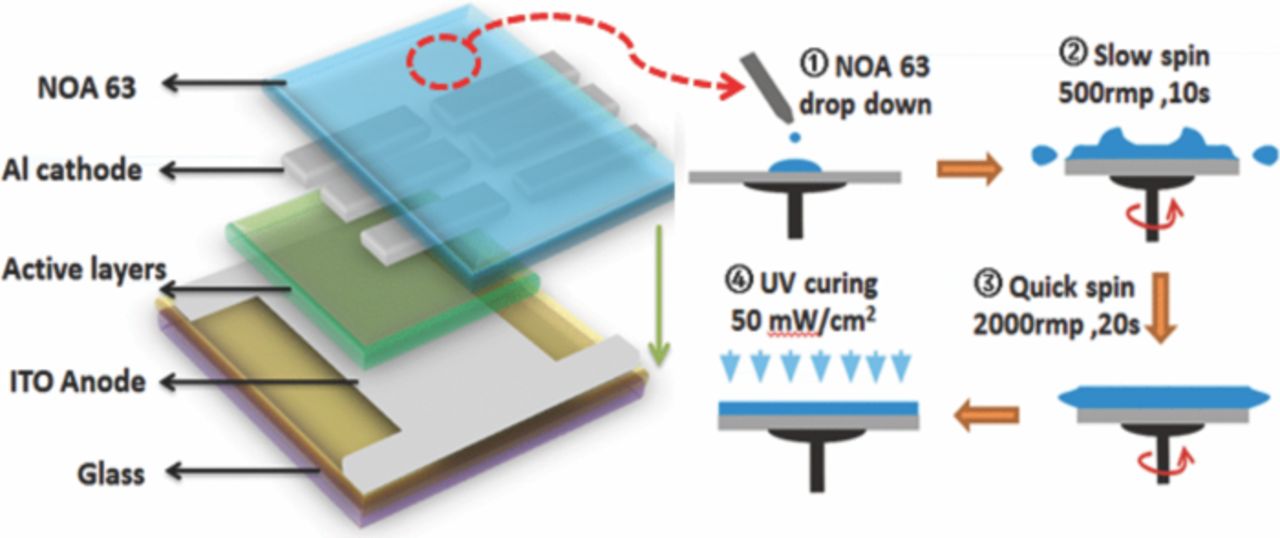
Figure 1. The test OLEDs sample structure: the active layers include MoO3/ m-MTDATA/NPB/ALq3 deposited by thermal evaporation. NOA63 passivation layer was formed by spin coating, its fabrication process is presented on the right side of the figure.
Results and Discussion
The L-V and the I-V characteristics were examined to compare the electrical behaviors of the device before and after encapsulation. As shown in Fig. 2a no notable difference in L–V between the bare device and the encapsulated devices was observed. The turn-on voltages for bare, GCE and NOA63 TFE devices were 3.22 V, 3.35 V and 3.35 V, respectively. All devices showed a luminance of 100 and 1000 cd/m2 at 5.8 and 8.1 V, respectively. Although, in the Fig. 2b, I–V profile of the NOA63 TFE device shifted to high dc voltage, substantial variations in luminance properties were not obvious. In addition, the peaks of EL spectra (not shown in this work), kept steadily at 520 nm, and they were independent on the driving voltage and encapsulation structures. Consequently, the aforementioned phenomena indicated our encapsulation, especially NOA63 TFE that is known to be UV curing and liquid-solid transformation process, did not cause any physical and chemical damages to the OLEDs.
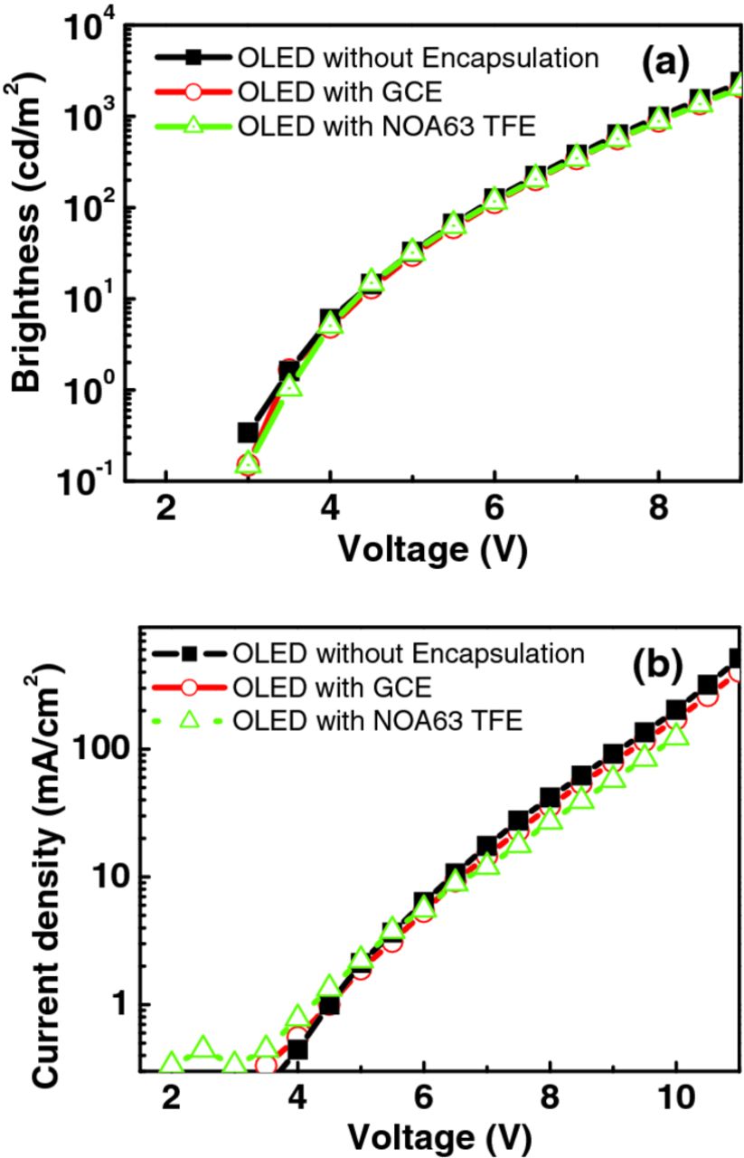
Figure 2. (a) Luminance–voltage and (b) Current–voltage vs. operational voltage characteristics for the bare OLEDs and encapsulation structure of GCE, NOA 63 TFE.
Fig. 3 showed the typical plot of normalized luminance versus operating time for OLEDs with various encapsulations at 20°C and 50% relative humidity testing condition. All luminance measurements versus operating time were carried out non-stop at a dc voltage of 8.1 V. The OLEDs were burned in for 100s to minimize the increase in brightness immediately after turn-on. The lifetimes of the devices were measured from an initial luminance of L0 = 1000 cd/m2. In this work, we defined the lifetime as the decay time of luminance to L/L0 = 0.7, which means the elapsed time of the instantaneous luminance of the OLEDs reaching at 70% of its initial value. As shown in Fig. 3, the lifetime of devices with encapsulation structure was much longer than that of the bare one. The GCE-device, had a lifetime of 2970 min, was comparable with device measured in the nominally O2/H2O-free glove-box. Generally, the luminance decay curves showed gradually decreasing behavior with operating time because of devices inherent instability.13 Considering no desiccant inside GCE structure, the slowly decay curve indicated that NOA63 adhesive exhibits good adhesion to the glass and thimbleful O2/H2O permeating through it from the device perimeter. Thus, remarkable gas barrier performance can be anticipated when using NOA63 as TFE. OLEDs with NOA63 TFE substantially achieve to be 1860 min in comparison 6.8 fold longer than that of the bare device.
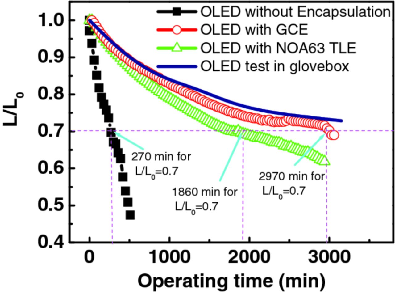
Figure 3. Normalized luminance (L/L0) as a function of continuous operation at 20 °C, 50% RH for the OLEDs with various encapsulations.
To evaluate the permeability of NOA63 film as a water diffusion barrier, water vapor transmission rate (WVTR) measurements were performed by calcium (Ca) corrosion test method.14 The permeability is characterized by using the calcium degradation by monitoring a resistive change in an Ohmic behavior. Fig. 4 showed a plot of the conductance changes with operation time for a Ca corrosion test device, whose schematic diagram was displayed in the inset of Fig. 4. 200 nm Ca layer with area of 1 × 1 cm2 was deposited on clean glass with 120 nm patterned Al as electrodes. The electrical measurement performed with two electrodes connected by a two-point probe SMU to an Agilent 2920 source meter. According to decreasing trend of conductivity with operational time, the lag time of 16 um-thick NOA63 film was 760 min at 20°C, 50% relative humidity condition under standard atmospheric pressure. The corresponding diffusion and solubility coefficient derived from lag time were 9.36 × 10⁻¹² cm2/s and 0.527 g/cm3/atm, respectively. The WVTR of NOA63 TFE was derived to be 0.031 g/m2day, which was among the lowest obtained by single polymer/organic passivation layer, the calculation details was describe in other reports.15,16 We attributed such low water permission rate to the fact that NOA63 is mercapto ester-type solvent-less prepolymer,17 allowing moderate UV-curable cross-linking process, which resulted in lower density of statistical defects. There is a microcosmic observation by AFM Dimension 3100 from Veeco (shown in Fig. 5), 16 um-thick layer possessed an average root-mean-square roughness of 1.2 nm, and the maximum difference in height (peak-to-valley) is about 1.9 nm. This "flatness" film is similar to those reported by several other investigators, who have shown that liquid monomer generated super smooth surface.7,8 Furthermore, topographical SEM image displayed in Fig. 6, showed the surface of the NOA63 film appears unstructured and almost homogeneous. It indicated NOA63 TFE lead to insignificant changes to the under-layer during solid-liquid transformation process. Hammond et al. reported that the remarkably tensile storage modulus of NOA63 (16.2–22.9 MPa) increased linearly, guaranteed a dense network cross-linked elastomeric structure continues to form on top of the under-layer.18 However, this solidification effect gets severely when a thermal-curing of polymer PDMS (2.4–4.5 MPa, Sylgard184, Dow Chemical) was formed. As showed in the inset of Fig. 6, 20 um-thick PDMS film results large wrinkles texture by several micrometers, which caused potential mechanical damages to the test samples.
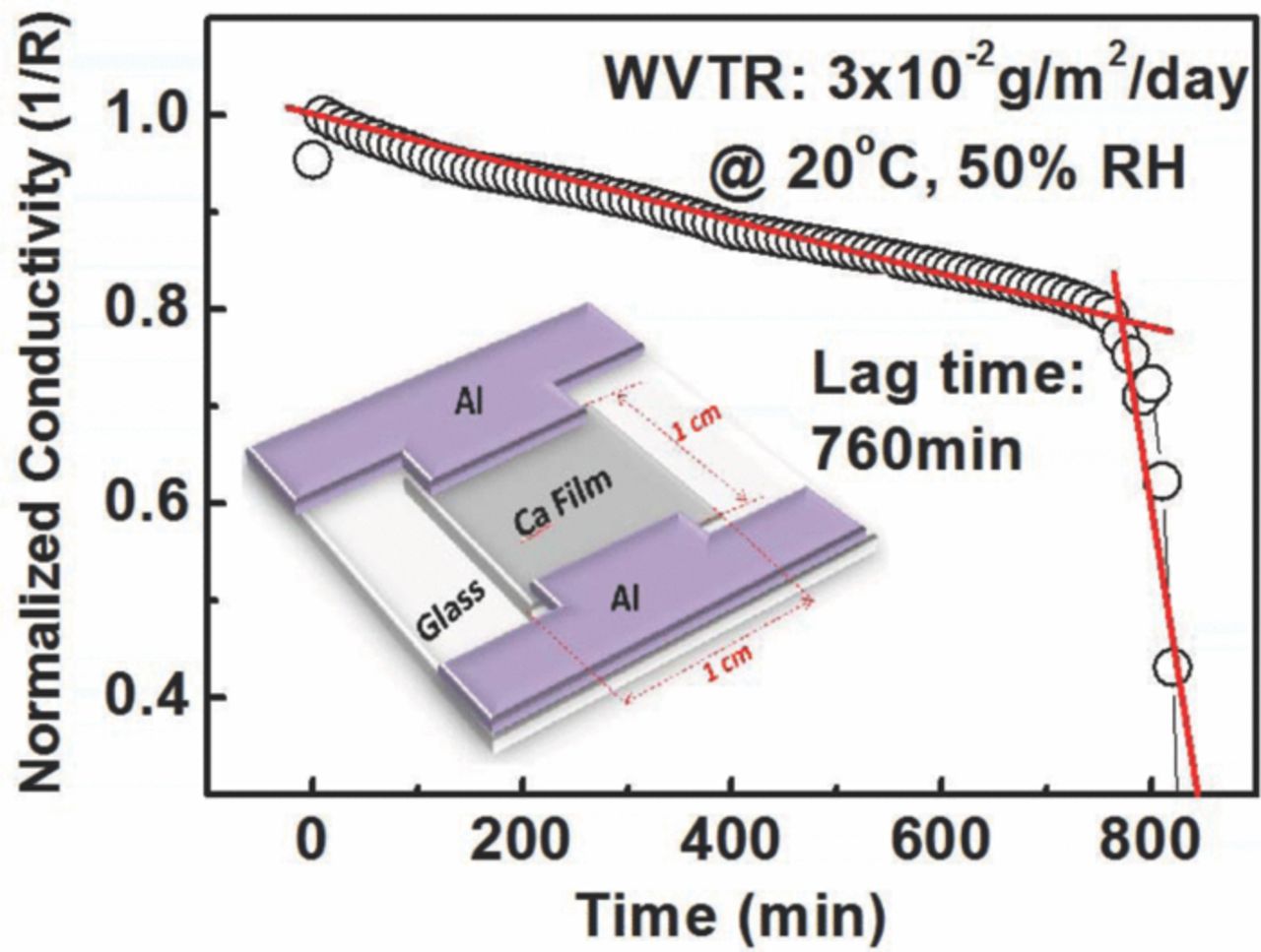
Figure 4. Ca corrosion test result of NOA63 water diffusion barrier structure at 20°C and 50% RH, the inset show the schematic Ca corrosion test setup for WVTR measurement.
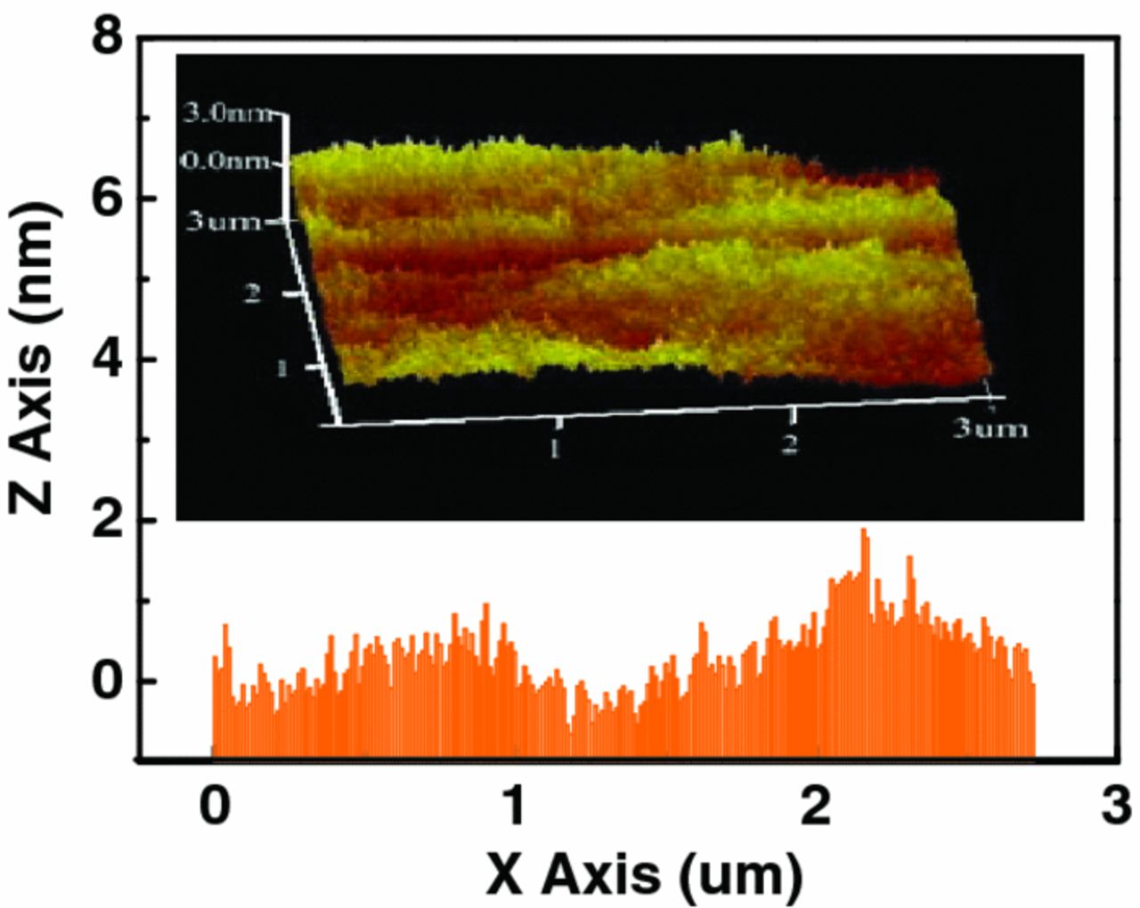
Figure 5. The surface morphology image of NOA63 TFE took by atomic force microscope.
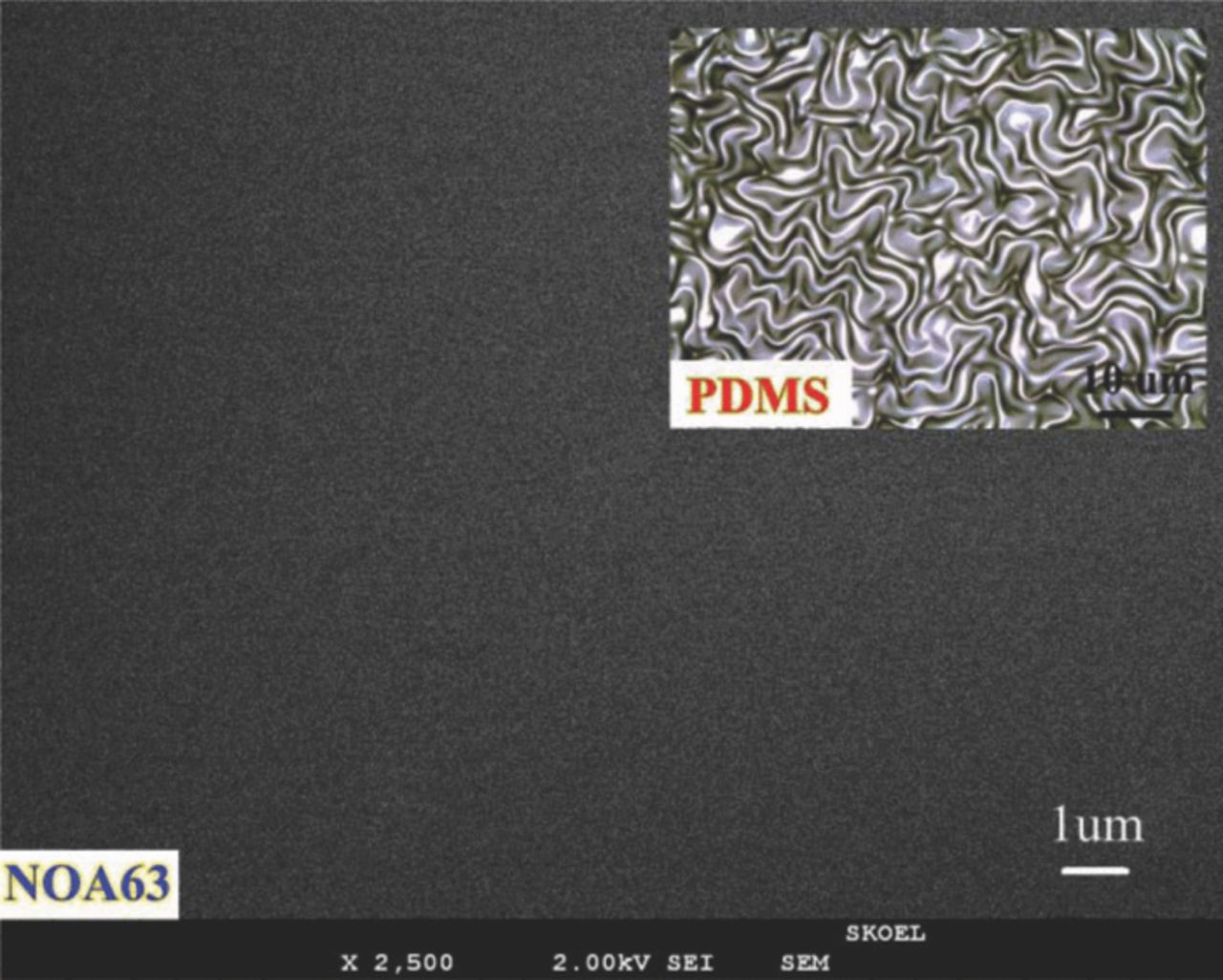
Figure 6. The topographical scanning electron microscope image of the NOA63 film, and optical microscopy image of the PDMS film was also presented on the top-right of the figure.
Summary
The simple TFE based on commercial NOA63 polymer has been carried out for the first time. No distinct deterioration in electrical properties of OLEDs was found after the NOA63 film formation. The permeability of the NOA63 film to water vapor was of 0.031 g/m2 and OLED encapsulated using the NOA63 TFE showed 6.8 folds continuous operation under identical environmental and driving conditions compared with devices that are not encapsulated. Although encouraging, we have to point out that the NOA63 TFE structure could make a certain extent improvement for OLEDs stability in air, but its barrier effect was still not match for devices using glass cap. At the present stage, our method would be using for short-time storage of organic electronics or as an elementary barrier before proceeded with high-ranking encapsulation.
Acknowledgment
This work was supported by National High Technology Research and Development Program of China (Grant No. 2011AA03A110), Ministry of Science and Technology of China (Grant No. 2010CB327701, 2013CB834802), the National Natural Science Foundation of China (Grant Nos. 61275024, 61274002, 60907013 and 41001302), Scientific and Technological Developing Scheme of Jilin Province (Grant No. 201101034), the Research Fund for the Doctoral Program of Higher Education (Grant No. 20070183088), the Opened Fund of the State Key Laboratory on Integrated Optoelectronics No. IOSKL2012KF01.