
Abstract
By controlling the different initial time of Hf and Al precursor supply, the proposed HfxAlyOz tunneling layer with different Al/Hf ratios from 0.21 (top) to 0.06 (bottom) can be fabricated. Regarding Al/SiO2/Pd nanocrystals/proposed HfxAlyOz/Si, the proposed HfxAlyOz film can prevent stress from Pd nanocrystals and achieve a higher electron current during programming. Regarding the retention characteristics, the final memory windows of 2.5/2.05 V at 25/90°C can be obtained, respectively. Programmed and erased with ±10 V/100 ms, the device shows a memory window of 2.4 V after 104 cycles for a 25°C test.

This is an open access article distributed under the terms of the Creative Commons Attribution 4.0 License (CC BY, http://creativecommons.org/licenses/by/4.0/), which permits unrestricted reuse of the work in any medium, provided the original work is properly cited.
Regarding high-k dielectrics, HfO2 shows a higher dielectric constant as compared to SiO2.1–3 However, the crystallization temperature of HfO2 is very low and easily results in a higher leakage current. Previous research indicated the crystallization temperature of HfO2 can be significantly increased by adding Al to the film.4 Moreover, adding Al to HfO2 is found to increase the Si/dielectric interfacial stability.5 Regarding memory application, HfxAlyOz film was served in the storage layer of the nonvolatile memory (NVM) device and good memory characteristics were achieved.6 Previous studies showed the embedded metal nanocrystals (NCs) in the dielectric of a NVM device improved the data retention characteristics.7–11 However, previous study reported that a huge stress induced by metal NCs in the SiO2 tunneling layer led to a worse retention characteristic and a small memory window because of many shallow traps in the SiO2 tunneling layer. Therefore, to reduce the shallow traps induced by metal NCs was an important issue.12 A high density of Pd NCs was easily formed on the HfxAlyOz tunneling layer, so the NVM with Pd NCs storage layer was also studied.12-13 Instead of SiO2, the HfxAlyOz was served as the tunneling layer, the retention characteristic in Pd NCs NVM device was improved.12 However, the induced shallow traps in the HfxAlyOz tunneling layer still affect the retention characteristics. In this paper, less shallow traps in the proposed HfxAlyOz tunneling layer could be achieved by a simple timing technique. The NVM device with proposed HfxAlyOz film will show better memory characteristics as compared to previous tunneling layer.
Experimental
HfxAlyOz films with different Al/Hf ratios (0, 0.12 and 0.278) were deposited on p-type Si substrate at 500°C by using combinations of Hf[OC(CH3)3]2[C5H11O2]2 and Al[PCH(CH3)2]3 precursors in metal organic chemical vapor deposition (MOCVD) system. Two precursors were injected into a pre-chamber, and then the precursors were vaporized and supplied into the main chamber by O2 gas at 1500 sccm. Al/Hf ratio in HfxAlyOz film was related to respective injected times into pre-chamber. The main chamber pressure was set at 5 mbar. As shown in Fig. 1a, an interfacial layer was obtained at HfxAlyOz/Si interface. These deposited samples were called HfO2, HfAlO-1 and HfAlO-2, respectively. After HfxAlyOz deposition, a thin Pd layer was set at 2 nm and deposited by using an E-gun system (3 × 10⁶ Torr, 40 mA and 0.02∼0.03 nm/sec). After Pd deposition, all samples were annealed with rapid thermal annealing at 500°C for 30 sec. Then, these samples were followed by a 30-nm-thick SiO2 blocking oxide deposition in plasma enhanced CVD system. The gases, power, pressure and temperature were SiH4/N2O/N2 (8.5/710/161.5 sccm), 20 W, 1Torr and 300°C, respectively. The photolithography process was conducted and Al (200 nm) was deposited as the top electrodes by a lift-off technology. There was a N2 annealing at 400°C after the deposition of the Al gate. In addition, some Al/Pd NCs/HfxAlyOz/IL/Si structures without blocking oxide deposition were also manufactured to compare programming current densities with one another. The energy band diagram of Al/SiO2/Pd NCs/HfxAlyOz/IL/Si structure during program operation is shown in Fig. 1b. In Results and discussion section, this energy band diagram will be used to explain the tunneling behavior.13 The capacitance-voltage (C-V) measurements were performed by a precision LCR meter of HP 4284A. In addition to LCR meter, the current measurement needs an HP 4155C parameter. The charge retention measurement adopts the C-t method.14 Pd nanocrystals on different HfxAlyOz films were inspected by transmission electron microscope (TEM) analysis. The chemical compositional analyses were conducted by Auger electron spectroscopy (AES). Regarding the HfAlO-1 film mentioned above, two precursors have the same supply time (15 sec) and initial supply time. However, for the proposed HfxAlyOz film, Hf[OC(CH3)3]2[C5H11O2]2 precursor was first supplied and there was a 2 sec delay for the supplied Al[PCH(CH3)2]3 precursor. Finally, the NVM device with the proposed HfxAlyOz film will be fabricated and characterized.
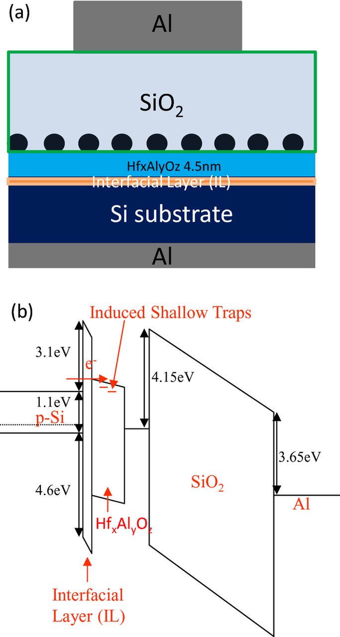
Figure 1. (a) Cross-sectional schematic of Al/SiO2/Pd NCs/HfxAlyOz/IL/Si (b) Energy band diagram of the structure with an interfacial layer during program operation.
Results and Discussion
Pd NCs can be observed on each HfxAlyOz film and the Pd NCs on HfAlO-1 film are shown in Fig. 2a. The density of Pd NC on each HfxAlyOz film is about 1.8–2.0 × 10¹²/cm2. The cross-sectional TEM image of SiO2/HfAlO-1/IL/Si is shown in Fig. 2b. The current density of Al/SiO2/Pd NCs/HfxAlyOz/IL/Si structure is much lower than that of Al/Pd NCs/HfxAlyOz/IL/Si by at least 5–6 orders of magnitude. Therefore, it is considered that the charging or discharging mainly occurs between Pd nanocrystals and the Si substrate through the HfxAlyOz tunneling layer concerning NVM device. Regarding all Al/SiO2/Pd NCs/HfxAlyOz/IL/Si structures, the typical C–V curves with the voltage swept from 8 to −8 V and then back to 8V are obtained, as shown in Fig. 2c. A larger hysteresis is observed in these C-V curves concerning Al/SiO2/Pd NCs/HfO2/IL/Si structure, but the smallest one concerning the sample with HfAlO-2. The shallow traps in the tunneling layer can be induced from Pd NCs and they play an important role in C-V hysteresis characteristic of the NVM device.12–13 According to the energy band diagram in Fig. 1b, when the voltage sweeps from 8 to −8 V, the electron is easily captured in the shallow traps of the tunneling layer and shows a positive shift in C-V curve. When the voltage sweeps from −8 to 8 V, it is easily relaxed from the shallow traps and shows a negative shift in C-V curve.15 It is considered that more induced shallow traps in HfxAlyOz film leads to a more obvious C-V hysteresis. Regarding C-V hysteresis (ΔVFB), the summarized table is shown in the inset of Fig. 2c. Therefore, HfxAlyOz film with higher Al/Hf ratio has a better immunity to the stress from Pd NCs and a smaller C-V hysteresis is observed. For Al/Pd NCs/HfxAlyOz/IL/Si, the summarized table of the current density at 0.8 V is shown in the inset of Fig. 2d. It reveals that the programming current density is lower concerning the HfxAlyOz film with a higher Al/Hf ratio. Due to introducing Al to the HfO2, it passivates the occupied VO gap states and reduces leakage current paths in the HfxAlyOz film.5 According to the discussion mentioned above, the NVM device with more shallow traps in HfO2 film shows a rapid drop at initial stage in retention characteristic and the least shallow traps in HfAlO-2 leads to a smallest variation of flatband voltage, as shown in Fig. 2e. Regarding initial/final memory windows, the summarized table is shown in the inset of Fig. 2e. Therefore, the HfxAlyOz film with a higher Al/Hf ratio can reduce shallow traps induced by Pd NCs to improve the retention characteristic and a lower Al/Hf ratio in the HfxAlyOz film can increase the programming current density. Regarding HfAlO-1 film, it is fabricated under the same supply time (15 sec) and initial time of Hf and Al precursors. Based on these results and discussion, the original process for HfAlO-1 film with Al/Hf ratio of 0.11–0.12 (in Fig. 3a) should be modulated. Regarding the proposed HfxAlyOz film, Hf precursor is supplied first, and then Al precursor is supplied with a 2 sec delay. As expected, Al/Hf ratio on the HfxAlyOz surface is 0.21, but only 0.06 near HfxAlyOz/IL/Si interfaces, as shown in Fig. 3b. Regarding the proposed NVM device, TEM image is shown in Fig. 4a. Owing to less induced traps in proposed HfxAlyOz film, it shows a small drop at initial stage in the retention characteristic and a final memory window of 2.5 V at 25°C. Moreover, a final memory window of 2.05 V at 90°C is also observed, as shown in Fig. 4b. Among 30 measured samples, the proposed NVM samples show that the memory windows vary from 2.3 to 2.6 V. In addition, the reliability of Al/SiO2/Pd NCs/proposed HfxAlyOz/IL/Si structure is also measured. The data endurance of the proposed memory device retains an obvious memory window of 2.4 V after 104 cycles and write/erase voltage is +/−10 V for 100 ms.
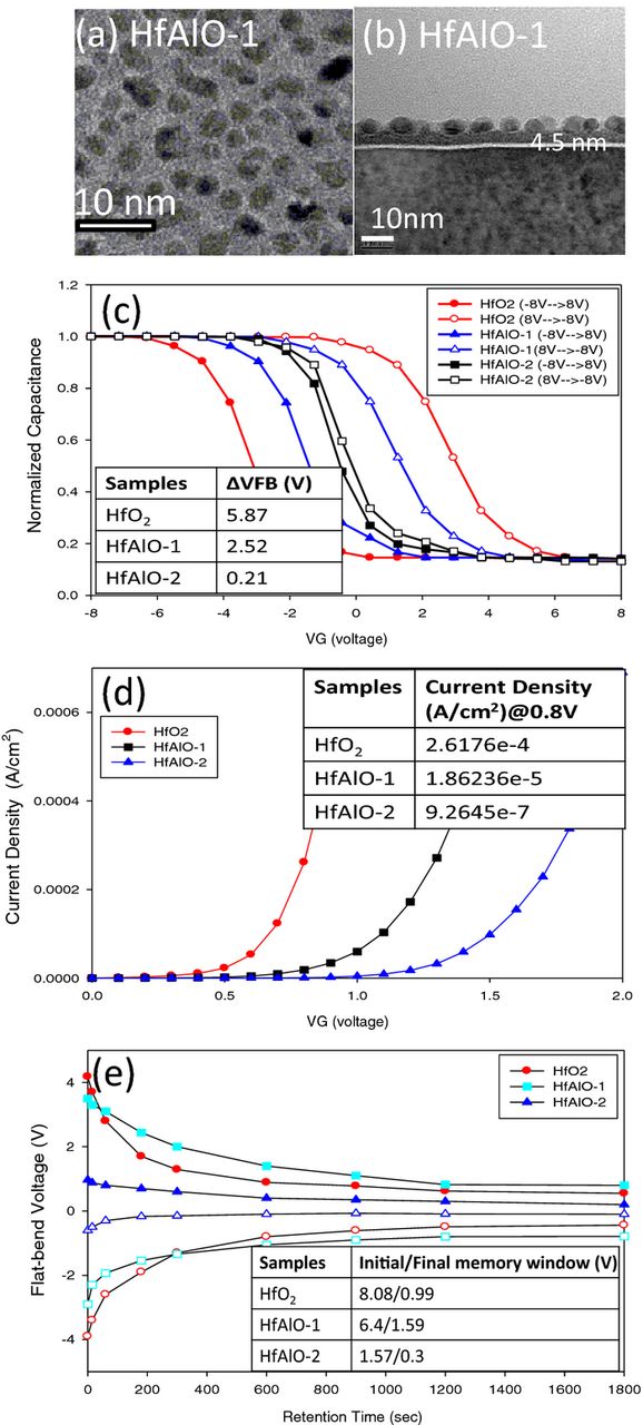
Figure 2. (a) TEM photograph of Pd nanocrystals on the HfAlO-1 film. (b) Cross-sectional TEM image of NVM with HfAlO-1 film. (c) Typical C–V curves with the voltage swept from 8 to −8 V and then back to 8V concerning all Al/Pd NCs/HfxAlyOz/IL/Si structures. (d) Current densities under gate bias concerning all Al/Pd NCs/HfxAlyOz/IL/Si structures. (e) Retention characteristics concerning all Al/SiO2/Pd NCs/HfxAlyOz/IL/Si structures.
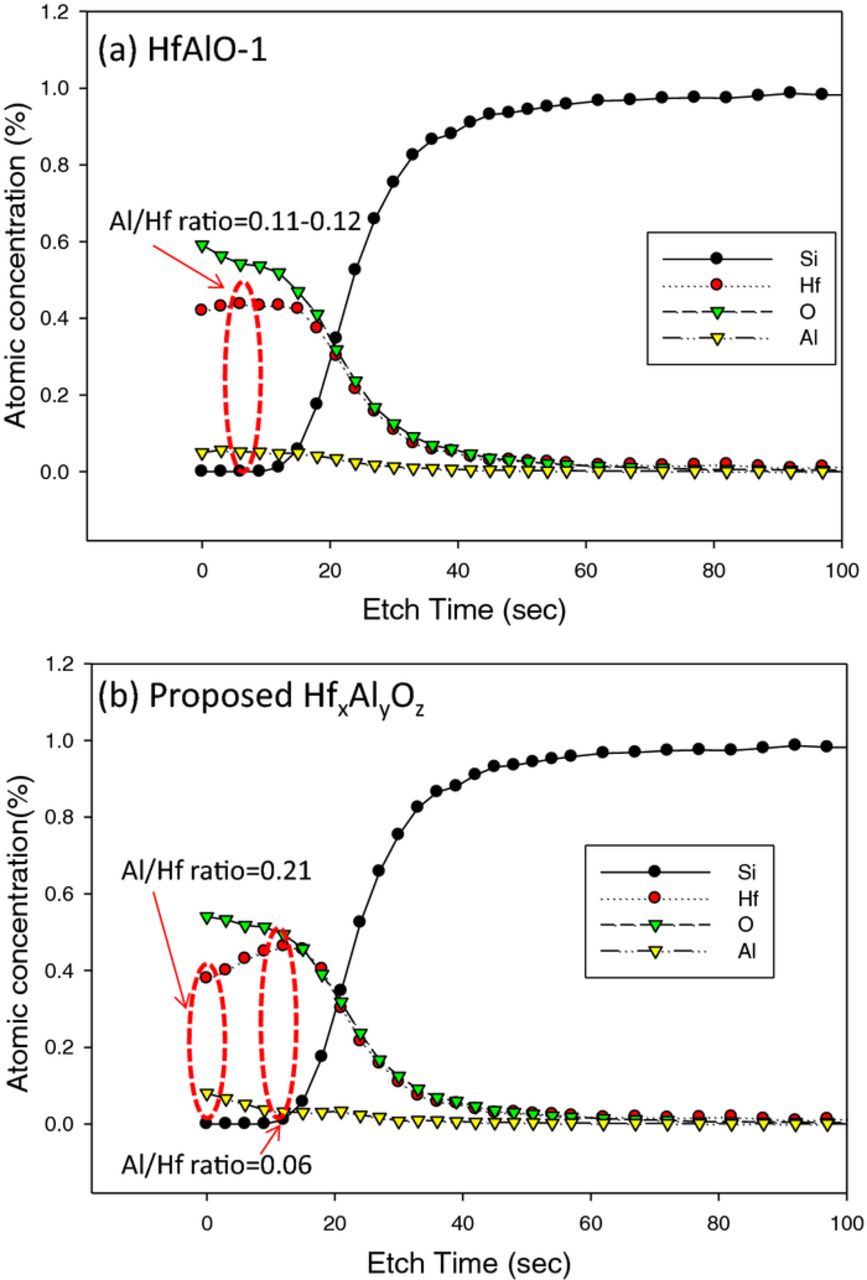
Figure 3. Chemical compositional analysis of the HfxAlyOz film under the same supply time and (a) without time delay (b) with a 2 sec delay concerning Al[PCH(CH3)2]3 precursor.
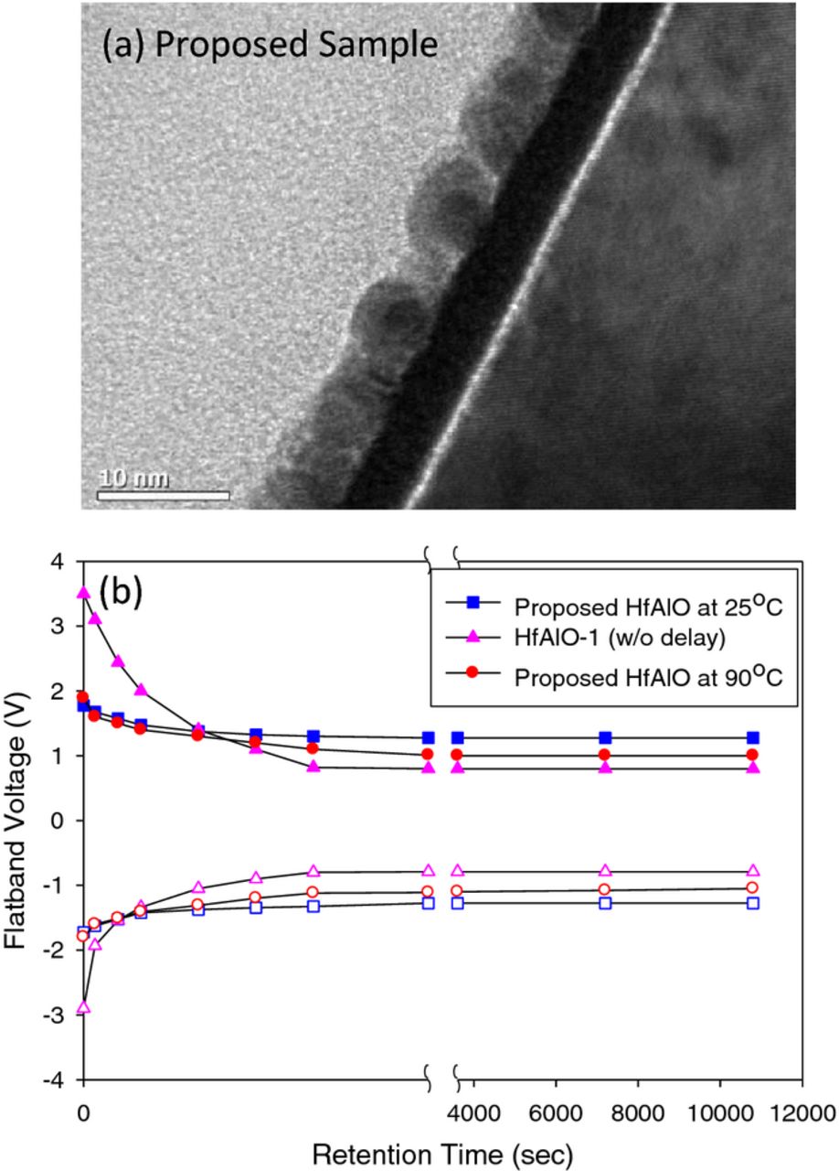
Figure 4. (a) Cross-sectional TEM image of NVM with proposed HfxAlyOz film. (b) Retention characteristics of the structures with/without delay concerning Al[PCH(CH3)2]3 precursor.
Conclusions
Different Al/Hf ratios from 0.21 (top) to 0.06 (bottom) in the proposed HfxAlyOz tunneling layer can be fabricated. When used in NVM device, this film has less shallow traps induced by Pd NCs and provides a higher tunneling current. Regarding the proposed NVM device, the final memory windows of 2.5/2.05 V at 25/90°C can be achieved, respectively. When programmed and erased with ±10 V/100 ms, the proposed NVM device shows a memory window of 2.4 V after 104 cycles for a 25°C test.
Acknowledgments
The authors acknowledge National Nano Device Laboratories (NDL) for their valuable technical support. This work is also supported by the Ministry of Science and Technology under contract No. MOST- 103-2221-E-035-082.